DISTORTION IN SINGLE PHASE CURRENT CONTROLLED
PV INVERTERS FOR GRID CONNECTION
R Sharma and T Ahfock Faculty of Engineering & Surveying University Of Southern Queensland
Toowoomba 4350.
Abstract
Unipolar switched single-phase inverters experience lower switching losses and cause less EMI when compared with bipolar switched inverters. However, these benefits come at the expense of increased distortion in the current waveform near the voltage zero-crossing. Moreover, it is demonstrated in this paper that switching delay causes generation of low frequency harmonics in the current waveform. In spite of that, unipolar switched inverters can be designed to operate within harmonic limits specified by the Australian Standard 4777.2.
1. INTRODUCTION
The conversion efficiency of single-phase, PWM, current controlled inverters can be improved by using unipolar switching [1]. Significant reduction in voltage transitions during switching is also an advantage from the point of view of EMI generation. The advantages of current control such as active current wave shaping, inherent current limitation, automatic synchronisation with the utility grid and elimination of lower order harmonics has been realised [2]. For simplicity and excellent dynamic performance characteristics the current loop may be based on hysteretic control [3].
It could be postulated that a unipolar switched inverter with hysteretic current control will have all the advantages listed above. But such inverters also have inherent problems that may need attention. These include:
(a) variation in the inverter switching frequency along the AC current waveform [4,5];
(b) increased distortion near the voltage zero crossing [6]; and
(c) generation of low frequency harmonics due to switching delay.
The last one of those problems is the focus of this paper. An analysis of hysteretic switching is carried out for both the unipolar switched inverter and the bipolar switched inverter. The objective of the analysis is to confirm that switching delay causes low frequency distortion in unipolar switched inverters with hysteretic current control.
The paper also explores the question of compliance to Australian Standard 4777.2.
2. INVERTER SYSTEMS
Figure 1 shows a simplified diagram of the inverter voltage control loop (VCL) and current control loop (CCL). The function of the VCL is to keep the DC voltage relatively constant. In doing so, balance between input DC power and output AC power is achieved. Increased insolation level will cause the bulk capacitor voltage vc to tend to rise. This in turn causes the DC voltage error ve and AC reference current isref to increase. The current controller provides switching signals for the inverter switches so that ip closely follows isref causing the AC power to rise and match the increased DC power.
Current control may be based on unipolar switching or bipolar switching.
2.1 Unipolar Mode
Hysteretic control with a fixed tolerance band, Itol, is used to force current ip to track the reference sinusoidal current isref. The controller forces the bridge into one of four possible states depending on the need to make
i
p rise or fall and on the polarity of vs. Wheneveri
p s falling and reaches the bottomcurrent limit,
i
p - 0.5Itol,i
p is made to rise by switching on TA+ and TB- if vs is positive or TB+ and TA- if vs is negative. Due to circuit component imperfections there is a time delay td between the instanti
p reaches the bottom current limit and the instant the inverter changes state (Figure 2). Wheneveri
p reaches the top current limit,p
i
+0.5Itol,i
p is made to fall by turning off one ofthere is a time delay between the instant
i
p reaches the top limit and the instant the inverter changes state.Figure 1: Single-phase grid connected PV inverter system.
[image:2.595.328.559.175.386.2](Is = peak of isref)
Figure. 2: Hysteretic current control
2.2 Bipolar Mode
Figures 1 and 2 are applicable. If we ignore blanking times the inverter operates in one of two states. Transistors TA+ and TB- are switched on when current
is reaches the bottom limit of the tolerance band. Transistors TB+ and TA- are switched on when current
is reaches the top limit. There is a time delay between the instant when isreaches a tolerance band limit and the instant the inverter changes state.
3. Low Frequency Distortion
SIMULINK® models were used to simulate unipolar and bipolar switching. Figure 3 shows the unipolar switching model and a similar model was developed for bipolar switching. The inverter switches were assumed to be perfect. An RLC ripple filter was added to filter out switching frequency harmonics (figure 4). The following values were used:
Vs= 240 V; Itol = 0.2 A; Vc = 400 V;
Iref = 4.0 A and 0.5 A; td= 2 µs and 8 µs;
CF= 2 µF; L1 = 8.0 mH; L2 = 2.0 mH ; Rc = 5Ω ; The rationale behind the choice of component values for the filter components is given in reference 5. That filter has practically no effect on low frequency harmonics.
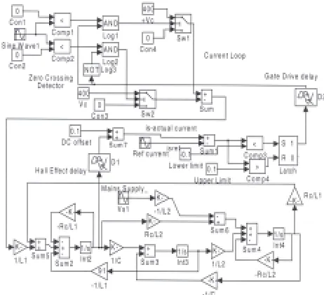
[image:2.595.77.294.298.428.2]Figure 3 SIMULINK model of the current loop
Figure 4: Ripple filter configuration
The time delay td represents a combination of component delays including current sensor, gate drive and main switching transistor. On grounds of power loss minimisation a Hall effect current sensor is preferred compared to a shunt resistor. However there is usually a need to keep cost down and this means that the quality of the selected Hall effect sensor will be such that it outputs a signal that is delayed. by, typically, a few microseconds compared with the actual current. The above values of td have been chosen to reflect this.
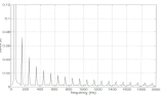
Simulation results are shown in figures 5 and 6. Harmonic analysis carried out on the current waveforms reveals significant levels of low frequency harmonics in the output of the unipolar switched inverter, whereas they are practically non-existent in
[image:2.595.328.540.428.509.2]the case of the bipolar switched inverter (figures 7 and 8).
(a) Inverter supplying 4.0 A
[image:3.595.359.518.87.183.2](b) Inverter supplying 0.5 A
Figure 5: Filtered output current from unipolar switched inverter
(a) Inverter supplying 4.0 A
(b) Inverter supplying 0.5 A
Figure 6: Filtered output current from bipolar switched inverter
(a) Unipolar Inverter supplying 0.5 A (td = 8 µs)
(b) Bipolar Inverter supplying 0.5 A (td = 8 µs)
Figure 7: Low Frequency current harmonics
4. Origin of Low Frequency Harmonics
Refer to figure 2. Reference current isref , the bottom limit of the tolerance band and the top limit of the band are all varying sinusoidally at power frequency. But over the relatively short duration of one inverter switching cycle, they can all be assumed to be straight lines. It is also assumed that is rises and falls linearly during a switching cycle. Based on those assumptions, expressions will be derived for iavwhich represents current ip averaged over one inverter switching cycle. Current iav, although averaged, is a function of time and may be regarded as current ip with all the switching frequency harmonics filtered by a ripple filter but with any low frequency harmonic remaining intact.
4.1 Unipolar Switching
During the rise time of ipwe have:
θ
sin ˆ
s V c V dt
p di
L = −
(1)
Therefore:
(
)
(
ˆ sinθ ωˆ cosθ)
sref I L s V c V c V d t tol LI r
t = + − − (2)
[image:3.595.344.519.212.327.2]θ sin ˆ s V dt di
L =− (3)
(
)
(
ˆ sinθ ω ˆ cosθ)
sref I L s V c V d t tol LI f
t = + + (4)
The ripple free current iav is given by:
L f t s V L r t s V c V r t f t r t av
i Isref Itol tdVs L
2 2 ) sin ˆ ( 2 2 ) sin ˆ ( ] {[ ) ( 1 )
( ˆ sin 0.5 ( ˆ sin )
θ θ
θ θ θ
− − + + = − − } ] [ˆ sin 0.5 ( ˆ sin ) f t L s V c V d t tol I ref
I θ+ + − θ
+ (5)
The following can be deduced from equation 5: (a) If switching delay is set to zero, not
surprisingly, current iav matches the reference current irefexactly.
(b) A non-zero switching delay results in iav being higher than ireffor half of the time and lower for the other half (figure 8) signifying the presence of low frequency distortion. (c) Percentage distortion due to low frequency
harmonics is much higher at lower output current (figure 8 (b)).
The fundamental reason for iav being higher than isref at lower values of vs is that ipis driven by a higher voltage, which is vc-
v
s , when it is rising above thetop tolerance limit compared to the voltage,
v
s , that drives ip when it is falling below the bottom limit. Similarly iav is lower than isref at higher values of vs because is is driven by a lower voltage, which is Vc-s
v
, when it is rising above the upper tolerance limit and by a higher voltage,v
s , when it is falling below the bottom limit.4.2 Bipolar Switching
During the rise time of ipwe have:
θ sin ˆ s V c V dt di
L = − (6)
Therefore:
(
2)
(
ˆ sinθ ω ˆ cosθ)
ref I L s V c V c V d t tol LI r
t = + − − (7)
Similarly during the current fall-time we have:
θ sin ˆ s V c V dt di
L =− − (8)
(
2)
(
ˆ sinθ ωˆ cosθ)
ref I L s V c V c V d t tol LI f
t = + + + (9)
The ripple free current iav is given by:
L f t s V c V L r t s V c V r t L s V c V d t tol I ref I f t r t av i 2 2 ) sin ˆ ( 2 2 ) sin ˆ ( ] ) sin ˆ ( 5 . 0 sin ˆ {[ ) ( 1 ) ( θ θ θ θ θ + − − + + − − + = } [ˆ sin 0.5 ( ˆ sin ) ]
f t L s V c V d t tol I ref
I θ+ + − θ
+
(10) The following can be deduced from equation 10:
(a) As in the unipolar case, if switching delay is set to zero current iav matches the reference current exactly.
(b) Current iav is always lower than isref with the difference at a given time instant being proportional to the value of isref at that instant. This signifies that although iav is lower than isref, there is no harmonic content in iav.
(c) The percentage difference between current iav and current isis higher at lower inverter output current (figure 9).
The fundamental reason for iav being lower than isref is that ip is driven by a lower voltage, which is Vc
-s
v
, when it is rising above the top tolerance limit and by a higher voltage, which is Vc +v
s , when it isfalling below the bottom tolerance limit. The difference between those two voltages is equal to twice vs, which is sinusoidal. This makes the difference between iav and is sinusoidal implying that iavis harmonic free.
0 0.5 1 1.5 2 2.5 3 3.5
0 0.5 1 1.5 2 2.5 3 3.5 4
(a) Inverter supply 4.0 A iav
0 0.5 1 1.5 2 2.5 3 3.5 0
0.05 0.1 0.15 0.2 0.25 0.3 0.35 0.4 0.45 0.5
[image:5.595.88.276.90.218.2](b) Inverter supply 0.5 A
Figure. 8: Unipolar Switched Inverter: Output Current with Switching Ripple Removed.
0 0.5 1 1.5 2 2.5 3 3.5
-0.5 0 0.5 1 1.5 2 2.5 3 3.5 4
(a) Inverter supply 4.0 A
0 0.5 1 1.5 2 2.5 3 3.5
-0.1 0 0.1 0.2 0.3 0.4 0.5 0.6
[image:5.595.351.514.102.199.2](b) Inverter supply 0.5 A
Figure. 9: Bipolar Switched Inverter: Output Current with Switching Ripple Removed
5. Practical Implications
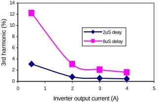
[image:5.595.86.269.268.533.2]Figure 10: Unipolar: Effect of delay on 3rd harmonics
Figure 11: Unipolar: Total harmonics Distortion An inverter selected for in grid-connected PV applications has to meet the requirements of a relevant standard that specifies distortion limits. In Australia this would be AS4777.2. The question is whether the levels of low frequency harmonics in the output of unipolar inverters fall within the limits specified by the standard. This question is best answered on a case by case basis. For the inverter considered in section 3 above, the third harmonic is the worst one and its levels are shown in figure 10. Total harmonic distortion is shown in figure 11. It has been assumed that non-zero switching delay is the only reason for the generation of low frequency harmonics. The inverter is designed for a rated output of 4 A, therefore it would satisfy the requirements of AS4777.2 even if switching delay is as high as 8 µs. Individual levels for the second to the ninth harmonic should be limited to 4% whereas total harmonic distortion should be limited to 5% [7].
6. CONCLUSION
Switching delay causes low frequency distortion in grid-connected unipolar switched inverters using hysteretic current control. A simple switching model has been used to explain how low frequency harmonics are generated. It has been shown that the unipolar inverter can still be designed to meet the requirements of AS4777.2. In spite of that, methods to reduce the percentage THD at low lower levels are currently being investigated.
7. References
[1]. Liaw C M, Chen T H, Wang T C, Cho G J, Lee C M and Wang C T, “Design and Implementation of a Single Phase Current-Forced Switching Mode Bilateral Converter”, IEEE Proceedings PtB, No.3, pp 129-136, May 1991.
[2]. Borle L, Dymond M S, Nayar C V, Philips S J, “Current Controlled Grid Connected Inverter”, Proceedings of the Australian and New Zealand Solar iav
isref
0 2 4 6 8 10 12 14
0 1 2 3 4 5
Inverter output current (A)
3r
d har
m
oni
c (
%
)
2uS deay 8uS delay
iav iav
isref isref
0 5 10 15 20 25
0 1 2 3 4 5
Inverter Output Current (A)
% T
H
[image:5.595.92.252.618.721.2]Energy Society Conference, pp 374-379, December 1993.
[3]. Harashima F, Inaba H, Kondo S, Takashima N, “Microprocessor-Controlled SIT Inverter for Solar Energy Systems”, IEEE Transactions on Industrial Electronics”, pp 50-55, Vol 34, No. 1, February 1987.
[4] Szepesi T, “Stabilising the Frequency of Hysteretic Current-Mode D.C./D.C. Converters”, IEEE Transactions on Power Electronic, pp 302- 312, Vol 2, No. 4, October 1987.
[5] Sharma R, “Switching Frequency Filter Design For Utility Connected PV Inverters”, Australasia Universities Power Engineering Conference Proceedings, September-October 2002.
[6]. Sharma R, “Analysis of PWM Transformerless Inverter for Utility Connected PV Applications”, Australasia University Power Engineering Conference Proceedings, September 2001.