This is a repository copy of Evaluating the Effect of Using Precision Alignment Dowels on
Connection Repeatability of Waveguide Devices at Frequencies from 750 GHz to 1.1 THz.
White Rose Research Online URL for this paper:
http://eprints.whiterose.ac.uk/88287/
Version: Accepted Version
Proceedings Paper:
Ridler, NM and Clarke, RG (2014) Evaluating the Effect of Using Precision Alignment
Dowels on Connection Repeatability of Waveguide Devices at Frequencies from 750 GHz
to 1.1 THz. In: Microwave Measurement Conference (ARFTG), 2014 84th ARFTG. 84th
ARFTG Microwave Measurement Conference, 04-05 Dec 2014, Boulder, Colorado. IEEE ,
1 - 10. ISBN 978-1-4799-7084-1
https://doi.org/10.1109/ARFTG.2014.7013405
[email protected] https://eprints.whiterose.ac.uk/ Reuse
Unless indicated otherwise, fulltext items are protected by copyright with all rights reserved. The copyright exception in section 29 of the Copyright, Designs and Patents Act 1988 allows the making of a single copy solely for the purpose of non-commercial research or private study within the limits of fair dealing. The publisher or other rights-holder may allow further reproduction and re-use of this version - refer to the White Rose Research Online record for this item. Where records identify the publisher as the copyright holder, users can verify any specific terms of use on the publisher’s website.
Takedown
If you consider content in White Rose Research Online to be in breach of UK law, please notify us by
Evaluating the Effect of Using Precision Alignment Dowels on
Connection Repeatability of Waveguide Devices at Frequencies
from 750 GHz to 1.1 THz
N M Ridler
1and R G Clarke
21
National Physical Laboratory, UK;
2University of Leeds, UK
Abstract—This paper describes an investigation into the effects of using additional precision alignment dowel pins on the connection repeatability performance of waveguide interfaces at submillimeter-wave frequencies. The waveguide interface type that was used for this investigation is an adapted version of the ‘precision’ UG-387 (i.e. based on the MIL-DTL-3922/67 design), manufactured by Virginia Diodes, Inc. The investigation was undertaken in the WM-250 waveguide band (i.e. at frequencies ranging from 750 GHz to 1.1 THz). Connection performance is compared with and without the use of added precision dowel pins in the inner dowel holes of this flange type. The repeatability of the measurements is assessed using statistical techniques, in terms of the experimental standard deviation in both the real and imaginary components of the complex-valued linear reflection coefficient.
Index Terms—Measurement repeatability, Submillimeter-wave measurements, VNA measurements, Waveguide flanges, Waveguide interfaces, Waveguide measurements
1. INTRODUCTION
Two recent papers [1, 2] have presented investigations into the connection repeatability of some waveguide devices operating from 750 GHz to 1.1 THz (i.e. in the WM-250 waveguide size [3]). In both these earlier investigations, the waveguide flanges were aligned during connection using four alignment dowel holes and dowel pins situated on the front faces of the flanges. These alignment dowel pins are permanently fitted to the flanges. During the connection of two waveguide flanges, two dowel pins on one of the flanges fit into two dowel holes on the other waveguide flange, and vice versa.
This connection strategy follows the so-called UG-387 flange design (described in [4] and earlier editions, e.g. [5, 6], etc), which has been in existence for many years. However, the performance of this
flange design has long been known to be poor at high
millimeter-wave and submillimeter-wave
frequencies, where the relatively loose tolerances on the specified diameters of the dowel pins and dowel holes cause performance degradation in the electrical measurements (i.e. significant mismatch and lack of connection repeatability). This has led to various improvements being made to this original design by different manufacturers. These improvements can broadly be described as being of two types: (i) the use of tighter tolerances on the above-mentioned outer alignment dowel holes and dowel pins; and/or (ii) the inclusion of two additional inner alignment dowel holes situated immediately above and below the waveguide aperture. These inner alignment dowel holes allow additional dowel pins to be inserted into both flange faces during connection.
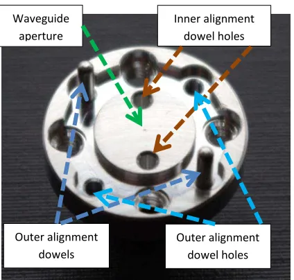
Fig. 1 shows a photograph of a flange that features both the outer dowel pins and dowel holes (used for the traditional UG-387 connection strategy) and the additional inner alignment dowel holes (to which additional dowel pins are inserted during connection). The other holes shown in this Figure (situated at north, south, east and west positions around the flange face) are threaded holes to enable screws to be used to tighten the connection between two flange faces.
The flanges used in the earlier investigations [1, 2]
feature both above-mentioned alignment
improvements. However, only the outer dowel pins and dowel holes were used for aligning the flanges during these earlier investigations.
Fig. 1. Waveguide flange showing the outer alignment dowel pins and dowel holes, and, the inner alignment dowel holes. The WM-250 rectangular
waveguide aperture is 250 m 125 m – barely
visible to the naked eye
The investigation described in this paper used the inner alignment dowel holes in conjunction with two different types of dowel pin:
(i) Typical dowel pins for use with these dowel
holes, found in some manufacturers’
calibrations kits;
(ii) Dowel pins that emulate a connection strategy that is being developed in a new IEEE standard [7]. This connection strategy uses dowel pins with different nominal diamaters. This paper compares the connection repeatability performance achieved using both the above types of dowel pins, and also compares the achieved performance with the connection repeatability performance reported previously in [2]. Flange connection performance is assessed by calculating the experimental standard deviation of a series of repeated flange connections. Results are presented as graphs showing experimental standard deviation versus frequency.
2. METHOD
2.1 Experimental set-up
The VNA system used for the investigation comprised an Agilent Technologies PNA-X VNA connected to WM-250 (WR-01) waveguide extender heads, manufactured by Virginia Diodes, Inc (VDI).
This is the same system and set-up that was used for the previous repeatability investigations [1, 2]. Following the procedure adopted in [2], the extender head was arranged so that the waveguide test port pointed vertically upwards. This arrangement minimizes any effect due to gravity on the alignment of the waveguide flanges. As with the previous investigations [1, 2], the power used to measure each Device Under Test (DUT) was around −35 dBm (0.3 W) and the VNA’s IF bandwidth was set to 30 Hz with no numerical averaging. The VNA system and set-up, shown in Fig. 2, is situated in the Roger Pollard High Frequency Measurements Laboratory (this being a temperature-controlled laboratory) at the School of Electronic and Electrical Engineering, University of Leeds, UK.
The VNA system was calibrated using a one-port ‘three-known-loads’ calibration technique. The ‘known loads’ (i.e. calibration standards) were an offset short-circuit, a ‘flush’ short-circuit and ‘near -matched’ load (from a VNA calibration kit supplied by VDI). The offset short-circuit and near-matched load were used subsequently as the DUTs for the repeatability investigation. It was not possible to use the flush short-circuit as a DUT for this investigation because the flange did not include the two inner alignment dowel holes. The offset short-circuit and near-matched load were the same DUTs that were used in [1, 2].
The connection repeatability procedure followed that given in [2], where the repeatability exercise includes connections of the DUTs where the orientation of the flange is inverted before being reconnected to the VNA test port. By inverting the waveguide flange, the imperfect position of the alignment dowel pins and dowel holes will, in principle, cause a systematic change in the VNA’s electrical measurements. This systematic change will be present in the repeatability data sets along with the random changes cause by the tolerances on the diameters of the alignment dowel pins and dowel holes.
[image:3.612.75.287.74.276.2]Fig. 2. The 750 GHz to 1.1 THz VNA system used for the measurements
2.2 Flange connection methods
(a) Same-diameter inner dowel pins: This flange connection method used two additional dowel pins inserted into the flanges’ inner alignment dowel holes. The two dowel pins used for this connection method were of the same nominal diameter. The purpose of this flange connection method is to emulate the conventional use of these inner alignment dowel holes. Some manufacturers supply these types of dowel pin in VNA calibration kits and so two such dowel pins (in this case, from a calibration kit manufactured by Flann Microwave Ltd) were used for this purpose.
A measurement of the diameter of both of these dowel pins, made using a digital micrometer, showed the diameter of one pin to be 1.555 mm and the other pin to be 1.556 mm.
(b) Different-diameter inner dowel pins: This flange connection method also used two additional dowel pins inserted into the flanges’ inner alignment dowel holes. However, for this connection method, each dowel pin was chosen to have a different diameter. This is to emulate the connection strategy being proposed for a flange design in a draft IEEE standard [7] that is currently under development. This strategy uses two dowel pins with different diameters. The dowel pin with the larger diameter achieves a very close fit to the flanges’ dowel holes and provides planar alignment for the waveguide apertures. This is called the “Planar Alignment Dowel” pin. The dowel pin with the smaller diameter achieves a looser fit to the flanges’ dowel holes and
provides angular alignment for the waveguide apertures. This is called the “Angular Alignment Dowel” pin.
The IEEE flange design uses inner dowel holes of a specific diameter, and associated dowel pins to fit these holes accordingly. The nominal diameter of the IEEE flange inner dowel holes is 1.570 mm. The nominal diameter of the IEEE flange Planar Alignment Dowel pin is 1.566 5 mm and the nominal diameter of the Angular Alignment Dowel pin is 1.556 mm.
The engineering drawing for the flange type used for the VNA test ports and DUTs (both manufactured by VDI), used in this exercise, is shown in Fig. 3. This Figure shows that the nominal diameter of the inner alignment dowel holes is 0.0625 inches (i.e. 1.588 mm) – i.e. this is not the same diameter that is proposed in the draft IEEE standard [7]. So it is not possible to follow exactly the connection strategy advocated by the IEEE standard for this particular flange design.
Fig. 3. Engineering drawing extract of the flange used for this investigation. The inner dowel hole diameter value (0.0625) is shown in the top right-hand corner of the drawing
[image:4.612.322.539.329.553.2]dowel holes – starting with the smallest diameter dowel pin and using increasingly larger diameter dowel pins until a diameter size was found that provided the closest fit to the dowel hole size. This dowel was then considered to perform a role similar to the Planar Alignment Dowel pin used for the connection strategy described in the draft IEEE standard [7]. A measurement, made using a digital micrometer, of the diameter of the selected dowel pin showed the diameter to be 1.586 mm. (The nominal diameter for the selected dowel pin was 1.590 mm, i.e. showing the measured value to be within 4 m of the nominal value.)
A second dowel pin was then selected with a nominal diameter of 10 m less than the Planar Alignment Dowel (i.e. with a nominal diameter of
1.580 mm). This 10 m difference in the pin
diameters is similar to the difference in diameter between the Planar and Angular Alignment Dowels used in the draft IEEE standard (i.e. 10.5 m). Therefore, the 1.580 mm diameter dowel pin was considered to perform a similar role as the Angular Alignment Dowel pin in the draft IEEE standard [7]. A measurement of the diameter of this dowel pin, made using a digital micrometer, showed the diameter to be 1.576 mm (i.e. within 4 m of the nominal value).
(c) No inner dowel pins: The repeatability exercise reported in [2] did not use the flange inner alignment holes for aligning the flanges during connection. Instead, only the outer alignment dowel pins and holes were used during that exercise. However, this earlier exercise used the same test port flanges and the same DUTs as used during this current investigation. Therefore, the results obtained in the earlier exercise [2] can be used to provide equivalent repeatability data for these flanges when used without the aid of the inner alignment dowel pins and holes.
2.3 Data Analysis
The analysis uses calculations of the
experimental standard deviation (as used previously in [1, 2]) as the measure of variability in the observed values due to flange connection repeatability. This computation is applied separately to both the real and imaginary components of the complex-valued linear reflection coefficient. An analysis based on using the magnitude and phase components of the reflection coefficient is avoided due to problems with such calculations that have been described in [8].
Let be the complex-valued linear reflection coefficient written in terms of its real, , and imaginary, , components as follows (with j2 = –1):
(1)
For n repeated determinations of , the arithmetic mean of is given by:
(2)
and the experimental variance is given by:
(3)
The experimental standard deviation, , is equal
to the positive square root of .
Similarly, the arithmetic mean of is given by:
(4)
and the experimental variance is given by:
(5)
The experimental standard deviation, , is equal
to the positive square root of .
For each DUT at each frequency, values of
and are calculated for the following three
situations:
(i) Using the 12 repeat measurements of the
flange when connected in the non-inverted orientation. Following the convention used in [2], we use a superscript N to indicate this ‘Non-inverted’ situation – i.e. for the real
component, and for the imaginary
component;
(ii) Using the 12 repeat measurements of the
flange when connected in the inverted orientation. Following the convention in [2], we use a superscript I to indicate this ‘Inverted’ situation – i.e. for the real
component, and for the imaginary
component;
(iii) Using all 24 repeated measurements of the flange connected in both inverted and
non-inverted orientations. Following the
convention in [2], we use a superscript IN to indicate this ‘Inverted and Non-inverted’ situation – i.e. for the real component, and
3. RESULTS
For each of the three flange connection methods, for both the offset short-circuit and the near-matched load, we can compare calculated values of the experimental standard deviations in the real
component, , and , and, we can
compare the calculated values of the experimental standard deviations for the imaginary component
, and .
This is shown in Figs. 4 to 15, where the labels ‘Same-diameter pins’, ‘Different-diameter pins’ and ‘No pins’ are used to identify the three flange connections methods described in sub-section 2.2,
i.e. (a) ‘same-diameter inner dowel pins’,
[image:6.612.323.537.69.249.2](b) ‘different-diameter inner dowel pins’ and (c) ‘no inner dowel pins’, respectively.
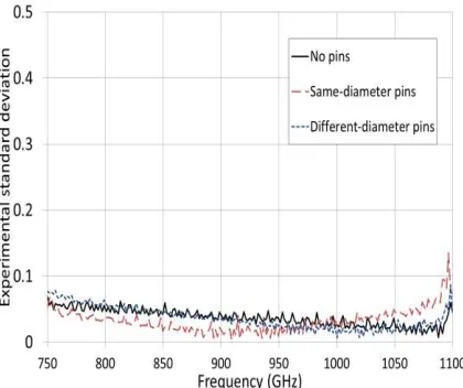
[image:6.612.74.286.288.465.2]Fig. 4. for the offset short-circuit
[image:6.612.325.537.289.463.2]Fig. 5. for the offset short-circuit
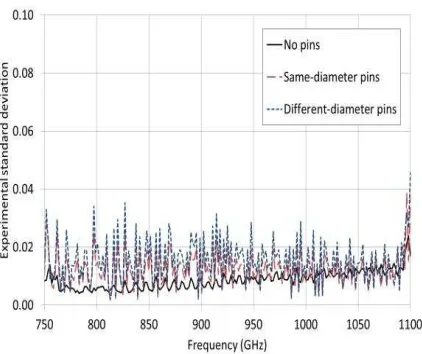
[image:6.612.75.285.505.681.2]Fig. 6. for the offset short-circuit
Fig. 7. for the offset short-circuit
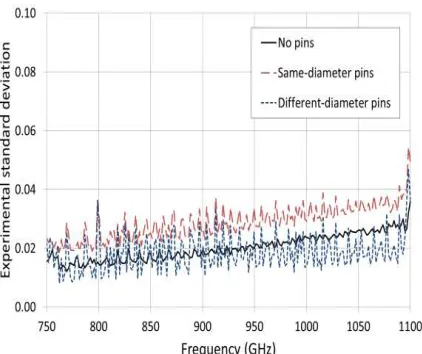
[image:6.612.327.537.513.679.2]Fig. 9. for the offset short-circuit
Fig. 10. for the near-matched load
[image:7.612.324.539.288.460.2]Fig. 11. for the near-matched load
[image:7.612.74.285.290.463.2]Fig. 12. for the near-matched load
Fig. 13. for the near-matched load
[image:7.612.75.286.502.679.2] [image:7.612.323.536.503.682.2]Fig. 15. for the near-matched load
4. DISCUSSION
The results presented in Figs. 4 to 15 show that, for all three flange connection methods, there is no clear and obvious ‘best’ connection method (in terms of the achieved standard deviations due to the repeatability of flange connections) for the situations examined in this investigation. There are some instances (e.g. in Figs. 6, 9, 13 and 15) where the connection using same-diameter inner dowel pins exhibits inferior repeatability. However, there are also instances (e.g. in Figs. 4 and 7) where the same connection method performs as good as, or better than, the other methods. Similar types of observation could be made about the other connection methods. There are also instances where flange connection repeatability for all three methods appears to be significantly worse than for other instances – see, for example, Figs. 6 and 9. However, this type of behaviour has been explained in a previous investigation [2], where this effect was attributed to imperfect positioning of the flange alignment dowel pins and holes, and so the waveguide apertures of the DUT and the VNA test port will be misaligned (systematically) by different amounts, depending on the orientation used for the connection of the DUT.
Since all three methods achieve quite similar connection performance, it is instructive to examine the methodologies behind these types of connection. As mentioned previously, the relatively loose tolerances that make the conventional UG-387 flange design [4-6] unacceptable for use at high millimeter-wave and submillimeter-millimeter-wave frequencies has led to two different strategies for improving this design:
1. Use tighter tolerance specifications for the outer alignment dowel holes and pins so that these holes and pins are suitable as the primary alignment mechanism for the flange;
2. Use inner alignment dowel holes and pins with
relatively tight tolerance specifications as the primary mechanism for achieving the required alignment precision. For these designs, the loose tolerance outer alignment dowel holes and pins remain as legacy features of the flange, but do not play a significant role in the alignment process.
[image:8.612.75.286.70.247.2]Table I summarizes the alignment properties for the conventional UG-387 flange design [4]. The table gives the specified range of diameter values for both the outer dowel holes and pins. These values are used to calculate a worst-case difference between these two diameters (i.e. between the largest hole-size and the smallest pin-size). This difference indicates how well the alignment pins fit the holes – the larger the difference, the worse the likely flange alignment. Table I shows a worst-case diameter difference for the UG-387 flange of 0.216 mm.
[image:8.612.320.548.368.469.2]
TABLE I
Diameters for the outer dowel pins and holes for conventional UG-387 flange Nominal (mm) Tolerance (mm) Range (mm)
Holes 1.702 +0.025, 0.000 1.7021.727
Pins 1.524 0.013 1.5111.537
Worst case diameter difference between pin and hole: (1.727 – 1.511) mm = 0.216 mm
[image:8.612.320.546.628.700.2]Table II shows similar information for the outer alignment dowel pins and holes for the VDI flange type used during the investigation reported in this paper. This information is derived from values given in Fig. 3 (although the values in Fig.3 are specified in inches). Table II shows a worse-case diameter difference for this VDI flange of 0.092 mm, which is considerably better than the conventional UG-387 flange summarized in Table I.
TABLE II
Diameters for the VDI flange outer dowel pins and holes Nominal (mm) Tolerance (mm) Range (mm) Holes 1.613 +0.008, 0.000 1.613 1.621
Pins 1.537 0.008 1.529 1.545 Worst case diameter difference between pin and hole:
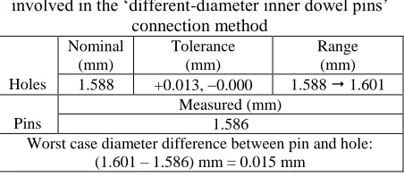
We can use a similar method to examine the alignment properties of the two connection methods described in this paper that used the inner dowel holes and pins. This information is shown in Tables III and IV for the ‘same-diameter inner dowel pins’ method and the ‘different-diameter inner dowel pins’ method, respectively. These tables show worse-case diameter differences of 0.046 mm for the same-diameter inner dowel pin method and 0.015 mm for the different-diameter inner dowel pin method. This would imply that the connection methods using the inner alignment holes and pins should provide better alignment than the use of the outer pins alone. However, the results from this investigation (in terms of achieved repeatability) suggest that the alignment provided by the tighter tolerance outer alignment dowel pins and holes for the VDI flange design is such that adding additional alignment mechanisms (i.e. using the inner alignment holes) does not improve significantly the overall alignment of the waveguide apertures. It therefore remains to be seen whether the connection strategy proposed in the new IEEE standard [7] (i.e. just using high-precision inner alignment holes and pins, along with loose tolerance outer holes and pins, as specified in the conventional UG-387 flange design) will result in improved connection repeatability compared to the repeatability performance obtained in this paper. The investigation of this type of connection strategy will need to wait until the flanges specified in the new IEEE standard [7] become available commercially and are used for
waveguide components operating at these
[image:9.612.320.546.98.197.2]frequencies.
TABLE III
Diameters for the inner dowel pins and holes involved in the ‘same-diameter inner dowel pins’
connection method Holes Nominal (mm) Tolerance (mm) Range (mm) 1.588 +0.013, 0.000 1.588 1.601
Pins
Measured (mm) 1.555 (and 1.556)
Worst case diameter difference between pin and hole: (1.601 – 1.555) mm = 0.046 mm
TABLE IV
Diameters for the inner dowel pins and holes involved in the ‘different-diameter inner dowel pins’
connection method Holes Nominal (mm) Tolerance (mm) Range (mm) 1.588 +0.013, 0.000 1.588 1.601
Pins
Measured (mm) 1.586
Worst case diameter difference between pin and hole: (1.601 – 1.586) mm = 0.015 mm
5. CONCLUSIONS
This paper has presented a detailed investigation and analysis of the connection repeatability performance that can be achieved from using waveguide flanges that are currently available on VDI waveguide extender heads for VNAs in the WM-250 waveguide size.
The investigation has concentrated on assessing likely improvements in connection repeatability due to the use of the inner alignment dowel holes found on these flanges. The use of different sizes of dowel pin has been evaluated as part of this exercise.
The results show that, for the flange types manufactured by VDI, there is no clear advantage, in terms of the achieved connection repeatability, in using these inner alignment dowel holes when making connections with these flange types.
It remains to be seen whether the use of the flange design that is currently being specified in the on-going draft IEEE standard [7] will improve upon the connection repeatability observed during this and earlier investigations [1, 2].
ACKNOWLEDGEMENT
The authors would like to thank Dr Jeffrey Hesler (Virginia Diodes, Inc) for helpful discussions concerning aspects of the VDI flange type used in this paper and for permission to use the engineering drawing shown in Fig. 3.
[image:9.612.67.297.529.616.2]REFERENCES
[1] N M Ridler and R G Clarke, “Investigating
Connection Repeatability of Waveguide
Devices at Frequencies from 750 GHz to 1.1 THz”, Proc. 82nd ARFTG Microwave Measurement Conference, pp 87-99, Columbus, OH, USA, Nov. 2013.
[2] N M Ridler and R G Clarke, “Further
Investigations into Connection Repeatability of Waveguide Devices at Frequencies from 750 GHz to 1.1 THz”, Proc. 83rd ARFTG Microwave Measurement Conference, pp 83-89, Tampa, FL, USA, June 2014.
[3] IEEE Std 1785.1-2012, “IEEE Standard for
Rectangular Metallic Waveguides and Their Interfaces for Frequencies of 110 GHz and
Above—Part 1: Frequency Bands and
Waveguide Dimensions”, Mar. 2013.
[4] “Detailed Specification Sheet – Flanges,
Waveguide (Contact) (Round, 4-hole)
(Millimeter)”, MIL-DTL-3922/67E with Amendment 1, May 2014.
[5] “Detailed Specification Sheet – Flanges,
Waveguide (Contact) (Round, 4-hole)
(Millimeter)”, MIL-DTL-3922/67C, June 2004. [6] “Detailed Specification Sheet – Flanges,
Waveguide (Contact) (Round, 4-hole)
(Millimeter)”, MIL-DTL-3922/67D, Dec. 2009. [7] IEEE Std 1785.2 (draft), “IEEE Standard for
Rectangular Metallic Waveguides and Their Interfaces for Frequencies of 110 GHz and Above—Part 2: Waveguide Interfaces”. [8] N M Ridler and M J Salter, “Evaluating and