The Amorphous-Crystal Interface in
Silicon: a Tight-Binding Simulation
The Harvard community has made this
article openly available.
Please share
how
this access benefits you. Your story matters
Citation
Bernstein, Noam, Michael J. Aziz, and Efthimios Kaxiras. The
amorphous-crystal interface in silicon: A tight-binding simulation.
Physical Review Series B 58(8): 4579-4583.
Published Version
http://dx.doi.org/10.1103/PhysRevB.58.4579
Citable link
http://nrs.harvard.edu/urn-3:HUL.InstRepos:2797694
Terms of Use
This article was downloaded from Harvard University’s DASH
repository, and is made available under the terms and conditions
applicable to Other Posted Material, as set forth at
http://
Amorphous-crystal interface in silicon: A tight-binding simulation
N. Bernstein and M. J. Aziz
Division of Engineering and Applied Sciences, Harvard University, Cambridge, Massachusetts 02138
E. Kaxiras
Division of Engineering and Applied Sciences, Harvard University, Cambridge, Massachusetts 02138 and Physics Department, Harvard University, Cambridge, Massachusetts 02138
~Received 13 February 1998!
The structural features of the interface between the cystalline and amorphous phases of Si solid are studied in simulations based on a combination of empirical interatomic potentials and a nonorthogonal tight-binding model. The tight-binding Hamiltonian was created and tested for the types of structures and distortions antici-pated to occur at this interface. The simulations indicate the presence of a number of interesting features near the interface. The features that may lead to crystallization upon heating include ^110& chains with some defects, most prominently dimers similar to those on the Si~001!231 reconstructed free surface. Within the amorphous region order is lost over very short distances. By examining six different samples with two inter-faces each, we find the energy of the amorphous-crystal interface to be 0.4960.05 J/m2.
@S0163-1829~98!00932-1#
I. INTRODUCTION
The crystalline and amorphous phases of silicon are con-sidered prototypical examples of a tetrahedrally coordinated network in ordered and disordered forms. Each phase has been intensively studied experimentally and theoretically, and both are used in a very broad spectrum of electronic applications. Currently all Si integrated circuits employ sev-eral ion implantation steps in their fabrication. Regions that receive a sufficiently high implantation dose become amor-phous within approximately 100 nm of the free surface; the crystal structure is restored by an interface-mediated crystal-lization process called solid-phase epitaxial growth~SPEG!. While much is known about the structure of the crystal and amorphous phases individually, considerably less direct in-formation is available about the structure of the interface between them. In light of the importance of SPEG, and of the intrinsic interest of interfacial phenomena, a detailed atomistic study of the amorphous-crystal interface in Si is appropriate. The inaccessibility of the interface atomic structure by experimental probes leaves as the only alterna-tive realistic simulations of this system. In this paper we discuss such simulations and the insight they provide into the atomic structure and dynamics at the amorphous-crystal in-terface in Si.
There are two major obstacles in simulating this interface: first, a relatively large number of atoms must be included in the simulation to ensure that the character of the two phases is represented accurately; second, extensive exploration of configuration space is required to ensure that the system is not locked in some small~and potentially not representative! region of the accessible configuration space. Ideally one would like to simulate this system by means of unbiased, parameter-free quantum-mechanical calculations @such as density funtional theory in the local density approximation
~DFT/LDA!#, but both the size of systems that can be handled and the extent of configuration space that can be
explored through such calculations are severely restricted. Past efforts have either used hand-built models,1,2computer relaxed geometrical models,3 or molecular-dynamics ~MD! simulations based on empirical interatomic potentials.4,5
Here we combine the use of the Stillinger-Weber empiri-cal interatomic potential and a recently developed semi-empirical quantum-mechanical technique, based on a non-orthogonal tight-binding ~TB!Hamiltonian that was param-etrized to represent accurately a wide range of bulk and sur-face structures of Si.6The use of the empirical potential was motivated by the fact that it affords fast but less accurate calculations for parts of the simulation where maintaining high accuracy is not important; specifically it is used to bring the system from a high-temperature, liquid-crystal interface far from equilibrium, to a low-temperature amorphous-crystal interface near equilibrium. Once the system is close to equilibrium, we switch to the TB model, which can handle reasonably large systems and is sufficiently fast to allow ex-ploration of configuration space, while maintaining the basic quantum-mechanical treatment of electronic degrees of free-dom. As such, it is superior to empirical interactions that are considerably more restricted in their ability to describe large structural distortions and the breaking and formation of co-valent bonds. The results of the tight-binding studies can also be used as starting points for more elaborate parameter-free quantum-mechanical calculations, although we anticipate that the essential features will remain unchanged.
II. METHODOLOGY
We use constant-temperature, constant-stress MD to pre-pare the amorphous-crystal interface samples starting with a liquid-crystal interface as described below. Because of the large time scale necessary to create reasonably equilibrated amorphous samples, the use of the tight-binding Hamiltonian to compute the interatomic forces while the system is very
PRB 58
far from its equilibrium state is impractical, and indeed not beneficial. Instead we use the Stillinger-Weber interatomic potential7to bring the system reasonably close to equilibrium and only then turn on the tight-binding Hamiltonian. The equations of motion are integrated with a Gear predictor-corrector algorithm8with a time step of 1 fs. The temperature is kept constant using a velocity rescaling algorithm where the atomic velocities are uniformly scaled to give the desired temperature once every 500 time steps. Zero stress is main-tained with an extended system Parrinello-Rahman approach.9
The simulation cell includes 320 atoms in a@220#3@22¯0#
3@005# box with periodic boundary conditions in all three directions. The interface lies in the (001) plane, with the
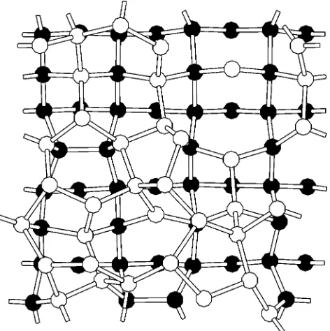
@220# and@22¯0#vectors forming its sides ~in the following the@001#direction is referred to as the z axis!. To create the interface, we maintain a portion of the simulation cell in the crystalline phase by keeping it below the melting point, while melting and then quenching the remainder of the cell. The crystalline region includes 128 atoms ~8 monolayers! that are kept at 100 K, and the remaining 192 atoms ~12 monolayers!form the amorphous region. The amorphous re-gion is produced by cooling a molten rere-gion from 5000 to 1000 K, using the method of Luedtke and Landman.10 A total of six samples, cooled to 100 K and equilibrated with the Stillinger-Weber potential, were relaxed using a conjugate-gradient algorithm with the tight-binding Hamil-tonian to calculate forces and stresses. The relaxed samples were used in the analysis of interface features. A typical sample is shown in Fig. 1.
III. ANALYSIS
Structural analysis
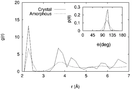
Standard measures for characterizing the structure of the bulk phases are the radial pair correlation g(r) and bond-angle distribution p(u) functions. These are shown in Fig. 2 averaged over all six samples. For the amorphous regions
~those that were thermally cycled!, the functions were com-puted from samples where the atoms in the crystal regions
~those that were kept cold! were removed, but using the original periodic boundary conditions. For the crystal regions the atoms in the amorphous regions were removed. Because of the missing neighbors at the edges of each region the normalization for the curves is nonstandard, although the overall shape is not affected. The pair correlation functions exhibit the expected features: averages over atoms in the crystalline regions show distinct order at all ranges allowed by the size of the simulation cell; averages over atoms in the amorphous regions show distinct first- and second-neighbor peaks, but no order at longer range. In particular, they do not have a third-neighbor peak, a feature also seen in DFT/LDA simulations11 and in experiment.12 In the following, the po-sition of the minimum between the first two peaks of the pair correlation function (r52.7 Å) is used as the criterion for defining the neighbors of an atom in the amorphous regions. The mean bond angles are 108.966° and 108.4614° in the crystalline and amorphous regions, close to the ideal tetrahe-dral angle of 109.5°.
Coordination statistics and ring statistics based on the same nearest-neighbor criterion are listed in Table I. The
coordination of the atoms in the crystalline region is nearly perfect; in the amorphous region there is a significant num-ber of defects, with overcoordinated atoms predominating. There is also a significant number of minimal rings ~ com-puted using shortest path analysis13!with size other than six, including a few eight-membered rings. In agreement with the results of DFT/LDA MD simulations by Stich et al.,11 we also observed more 5-membered than 7-membered rings. The total ring statistics indicate more even-membered rings than the random bond switching model of Wooten et al.,14,15 and fewer odd-membered rings.
The characterization of the interface is somewhat more demanding. In order to identify the interface region and to characterize its features we define three different quantities. The first of these is the rms deviation of the bond angles from the ideal tetrahedral angleDu. The bond angle
devia-FIG. 1. View of a sample along a (110) axis of the crystal. Atoms that were kept cool throughout the simulation~ correspond-ing to the crystalline region!are in black, atoms in the region that was heated and then cooled ~corresponding to the amorphous re-gion! are in white. Bonds are drawn between atoms closer than a distance of 2.7 Å. Periodic boundary conditions apply in all three directions.
tion for each atom versus its z coordinate, averaged over all samples and smoothed by averaging over a thickness
Dz51.0 Å, is plotted in Fig. 3~a!. Although the differences between the crystal and amorphous regions are small~due to the strong angular forces in silicon!, 7-Å-thick transition re-gions associated with the interfaces are clearly visible be-tween z55 and 12 Å, and between z517 and 24 Å. This observation is in contrast to results of Spaepen1 from an analysis of a hand built model for a (111) interface relaxed with a Keating potential that shows a larger bond angle de-viation at the interface than at either of the adjacent phases. A second quantity we define to characterize the interface is the sum of the vectors pointing from an atom to its nearest neighbors. This vector quantifies the asymmetry of the atomic environment. For example, if an atom is missing one of its neighbors while retaining s p3bonding, this vector will point away from the missing atom. We refer to this vector as the ‘‘tetrahedral vector’’vWt. Because of the difficulty of plot-ting vector quantities, the magnitude ofvWtversus the z posi-tion of each atom is plotted in Fig. 3~b!, averaged over all samples and smoothed as described earlier. The differences betweeen the crystalline and amorphous regions are again small but distinct. The extent of the interface usingvWtis very similar to that indicated by Du. In the interface region, both
Du and vWt vary monotonically between the values in the amorphous and the crystal regions. The definition of the
vec-tor sum becomes more useful when its values and directions at individual interface atoms are considered: these indicate the direction and amount by which a given atom ~or one of its neighbors!should move in order to create an environment closer to the crystalline state.
A third local quantity we employed to characterize the interface region is the volume of the Voronoi polyhedron associated with each atomVv, plotted in Fig. 3~c!, averaged over all samples and smoothed as described earlier. This quantity gives a local measure of the density, as well as an estimate of the free volume around each atom. Vv is about 19.0 Å3 in the crystal, which corresponds to a 3.5% com-pression of the unstrained bulk crystal volume. In the amor-phous region Vv ranges from 20.0 Å3 to 20.5 Å3, i.e., the amorphous phase is a few percent less dense than the crystal. To determine the variation of the strain with position and direction, we calculated the mean nearest-neighbor spacing projected along the in-plane axes, x and y , and the perpen-dicular axis, z. In the crystalline region the x and y spacings are 7% smaller than the spacing along the perpedicular di-rection, indicating that the crystal is under biaxial compres-sion. In the amorphous region the x and y spacings are 3% larger than in the perpendicular direction, indicating that the amorphous is under biaxial tension. Because the two adja-cent phases are in opposite strain states, it is impossible to resolve the sign or magnitude of the interface stress.
[image:4.612.339.526.55.312.2]FIG. 2. Measures of order in the bulk of the crystalline and amorphous regions ~as defined in the text!: Pair correlation func-tions g(r) and bond angle distribution funcfunc-tions p(u).
TABLE I. Coordination and ring statistics averaged over six samples. Coordination statistics are tabulated separately for the crystalline and amorphous regions. Note that the rings are too large compared to the thickness of the crystalline region to allow for such a separation, so values averaged over the entire sample are listed.
Coordination statistics
Neighbor num. 2 3 4 5 Crystal 0.1% 0.4% 98.6% 0.9% Amorphous 0.1% 3.2% 91.7% 4.9%
Rings per atom
[image:4.612.65.286.57.206.2]Ring Size 3 4 5 6 7 8 All rings 0.01 0.04 0.36 1.11 0.86 2.59 Minimal rings 0.01 0.04 0.36 0.99 0.25 0.01
FIG. 3. Local measures of order through the samples containing a crystal-amorphous interface, averaged over six samples. The or-dinate is the z cooror-dinate of atoms along the@001# direction of the crystal, which is normal to the interface.~a! Duis the RMS devia-tion of the nearest-neighbor bond angles from the ideal tetrahderal angle of 109.5 °;~b!uvWtuis the magnitude of the sum of the
nearest-neighbor vectors;~c! Vvis the Voronoi volume~volume of region
For a better understanding of the structure of the amorphous-crystal interface we created slices of the samples parallel to the interface. Perspective views of these slices reveal some interesting characteristics: Fig. 4 is an example where the prominent features of the crystalline portion are chains of atoms along the @110# direction, with very few defects. The atoms that are not in ideal positions form dimers, where pairs of atoms on adjacent@110# chains have come close together to form a bond, a feature that was also seen in the hand-built model of Saito and Ohdomari.2 One example of this defect is seen on the left side of the image in Fig. 4 ~between the two vertical@110# chains!. This feature is very similar to the well-known Si~001!231 free surface reconstruction, although in the present case the atoms par-ticipating in the dimer have four bonds~each with two more neighbors on the crystalline side and one more neighbor on the amorphous side!. On the amorphous side of the interface, some atoms are beginning to assume positions compatible with the crystal lattice. They line up in chains along @110# directions~top of image in Fig. 4!, as would be expected for the next layer in the crystal. The remaining atoms are ar-ranged in more disordered configurations.
IV. INTERFACE ENERGIES
One important quantity that characterizes the interface is the interfacial tensionsac, which is, for a single-component system, the excess free energy per unit area. This excess is responsible for the barrier to nucleation of the crystal in the middle of the amorphous phase; typically the interfacial ten-sion is determined experimentally by interpreting nucleation rate measurements under conditions where heterogeneous nucleation is believed to be insignificant. Because it is diffi-cult to ensure that this condition has been achieved, experi-mental values for the interfacial tension, such as those
esti-mated by Tsao and Peercy16 or Yang,17 represent a lower limit on the true value of the interfacial tension. At suffi-ciently low temperatures the entropic contribution to the in-terfacial tension can be neglected and sac can be approxi-mated by the excess interfacial energy per unit area «ac, which is easier to determine theoretically. Mathematically,
«ac is defined as the excess energy of a system with an interface over the weighted sum of the energies of the two constituent phases,
«ac5~E2Nc«c2Na«a!/A. ~1!
E is the total cohesive energy of the sample with the inter-face, «c and «a are the cohesive energies per atom of the reference crystal and amorphous states, Nc and Na are the number of atoms in the crystalline and amorphous phases, respectively, and A is the total area of the interface. An analogous equation to Eq. ~1! for sac can be obtained by replacing «c and «a by the corresponding free energies of these phases per atom, gc and ga. When the system is in equilibrium, the assignment of atoms to the individual phases
~i.e., the determination of Nc and Na) is unnecessary be-cause, by definition, gcand ga are equal in equilibrium. For the silicon amorphous-crystal interface, even when sac can be approximated by «ac, the determination of Nc and Na is necessary because the two phases are not in equilibrium with each other. Hence we must determine which atoms should be considered ‘‘crystalline’’ and which ‘‘amorphous.’’
To do that we visualize slices of our samples parallel to the interface and label as crystalline any atoms that are bonded to two atoms that were kept frozen or two other atoms that are labeled as crystalline by this procedure, pro-vided that the two atoms would share a common neighbor in the perfect crystal. This ensures that all the atoms that are considered part of the crystal are in a nearly ideal crystal environment on at least one side, and all are members of sixfold rings that are contained in the crystal. Because the calculated interface energy is sensitive to the number of crys-tal atoms we need to employ a more rigorous definition of the bond between atoms than the one used earlier, which relied simply on distance~atoms closer than 2.7 Å were con-sidered bonded!. To this end, we consider atoms bonded only if the tight-binding charge density half way between them is above a threshold value that is obtained by using representa-tive s and p orbitals attached to each atom. Typically, be-tween 10 and 20 pairs of neigboring atoms~out of about 650 pairs in each sample! have charge densities that fall below this threshold and are not considered to be bonded to each other, even though their distance is shorter than 2.7 Å.
A second complication in using our tight-binding Hamil-tonian to compute the interface energy is the precise value of
[image:5.612.58.294.58.295.2]«c and«a. The reference crystal state is an uncompressed diamond lattice ~the compression energy is negligible!, trivial to generate and its cohesive energy«cis easy to com-pute. To compute an appropriate reference amorphous state from which «a can be estimated, we take each interface sample and apply the same procedure we used to create the amorphous portion, but this time keeping a 4.75 Å slab cen-tered in the middle of the amorphous portion frozen. In this way, we make the entire sample amorphous. Each bulk amorphous sample is then relaxed with the tight-binding
FIG. 4. Plan view of an amorphous-crystal interface with the same colors as in Fig. 1. One dimer defect in the crystalline region near the bottom center of the image and one near the left center are easily seen.
Hamiltonian, and used as the reference state when computing the interface energy for the corresponding interface sample. The resulting bulk amorphous samples have cohesive ener-gies«a between 4.519 and 4.536 eV/atom, corresponding to an excess energy for the amorphous phase D«ac of 0.17 to 0.19 eV/atom. These values are a factor of two higher than an experimental value for D«ac of 0.097 eV/atom, as ex-trapolated to 0 K from Donovan’s measurement18 at 960 K using the specific heat listed in that work.
The resulting interface energies sac range from 0.39 to 0.54 J/m2 for the six different samples, with a mean of 0.49 J/m2and a standard deviation of 0.05 J/m2. The scatter is due to several factors. The total energy of the two inter-faces in each sample is a small number~about 15 eV! com-puted by subtracting large numbers ~total energies for the interface and reference states, each of order 1500 eV!. Scat-ter of 0.3% in the total energy of the inScat-terface samples or reference amorphous samples ~which is inevitable due to their disordered nature and small size of the systems!causes a scatter of 30% in the computed interface energy. Partition-ing the atoms into crystalline and amorphous parts also in-volves an error of about two or three atoms per interface, arising from both the threshold charge density value for con-sidering two neighboring atoms bonded and from errors made in the manual counting process. There is also a poten-tially larger source of error in the arbitrary definition of what is required for an atom to be considered ‘‘crystalline.’’ Some other criteria we considered, using the values of different measures of order to distinguish between ‘‘crystalline’’ and ‘‘amorphous’’ atoms, gave values for Nc that differed by as many as tens of atoms from the topological criterion de-scribed previously.
The only previous attempt to compute the interface en-ergy through simulation we are aware of is Spaepen’s work1 using a Keating potential to evaluate the energy of each atom in a hand-built model of a (111) interface; the computed interface energy was 0.31 J/m2. Saito and Ohdomari2 also computed the Keating potential energy as a function of dis-tance from the interface, although they did not publish a
corresponding interface energy. Using their plot of the ex-cess energy, and considering their ‘‘original surface’’ as a part of the crystal, we compute an interface energy of 0.23 J/m2. These values are consistent with our calculation considering the substantial differences in interface geometry and computational methods. The most recent experimental measurement of the amorphous-crystal interfacial tension for silicon we are aware of is by Yang:17an interfacial tension of 0.48 J/m2 was obtained by fitting a physically motivated kinetic model to the observed nucleation rate of crystals dur-ing ion-beam enhanced crystallization of an amorphous sample. The agreement of this value with our calcalution is excellent, but probably fortuitous. The only other experimen-tal result we are aware of is the work by Tsao and Peercy.16 They deduced an interfacial tension of 0.04 J/m2 from Ko¨-ster’s nucleation rate measurements for amorphous thin films,19 where the nucleation is unlikely to be homogenous, and is therefore not a reflection of the true interfacial tension.
V. SUMMARY
Using a combination of interatomic potentials and a spe-cially optimized nonorthogonal tight-binding Hamiltonian we have created amorphous-crystal interfaces in silicon by performing melt and quench numerical experiments. The in-terfaces are about 7 Å thick. All measures of order we con-sidered interpolated smoothly between the crystalline and amorphous values. Slices of the sample along the interface reveal features analogous to dimers on the Si~001! surface and short crystal-like chains in the amorphous layer adjacent to the crystal. By comparing the energies of samples with and without interfaces we compute an interface energy of about 0.49 J/m2, in good agreement with experimental evi-dence and other theoretical work.
ACKNOWLEDGMENT
This research was supported by the Harvard MRSEC un-der Contract No. NSF-DMR-94-00396.
1Frans Spaepen, Acta Metall. 26, 1167 ~1978!; F. Spaepen, in
Amorphous Materials, Modeling of Structures and Properties,
edited by V. Vitek~TMS-AIME, New York, 1983!, p. 265.
2T. Saito and I. Ohdomari, Philos. Mag. B 43, 673~1981!; T. Saito
and I. Ohdomari, ibid. 49, 471~1984!.
3F. Wooten and D. Weaire, J. Non-Cryst. Solids 114, 681~1989!. 4S. Erkoc, T. Halicioglu, and W. A. Tiller, J. Non-Cryst. Solids 94,
28~1987!.
5G. H. Gilmer and C. Roland, Appl. Phys. Lett. 65, 1~1987!. 6N. Bernstein and E. Kaxiras, in Materials Theory, Simulations,
and Parallel Algorithms, edited by E. Kaxiras, J. Joannopoulos,
P. Vashishta and R. Kalia, MRS Symposia Proceedings No. 408
~Materials Research Society, Pittsburgh, 1996!, p. 55; N. Bern-stein and E. Kaxiras, Phys. Rev. B 56, 10 488~1997!.
7F. H. Stillinger and T. A. Weber, Phys. Rev. B 31, 5262~1985!. 8M. P. Allen and D. J. Tildesley, Computer Simulations of Liquids
~Oxford University Press, Oxford, 1987!.
9M. Parrinello and A. Rahman, Phys. Rev. Lett. 45, 1196~1980!;
J. Appl. Phys. 52, 7182~1981!; J. Chem. Phys. 76, 2662~1982!.
10W. D. Luedtke and U. Landman, Phys. Rev. B 37, 4656~1988!. 11I. Sˇtich, R. Car, and M. Parrinello, Phys. Rev. B 44, 11 092
~1991!.
12S. Kugler, G. Molna´r, G. Peto¨, E. Zsoldos, L. Rosta, A. Menelle,
and R. Bellissent, Phys. Rev. B 40, 8030~1989!.
13S. V. King, Nature~London!213, 1112~1967!.
14F. Wooten, K. Winer, and D. Weaire, Phys. Rev. Lett. 54, 1392
~1985!.
15F. Wooten and D. Weaire, Solid State Phys. 40, 1~1987!. 16J. Y. Tsao and P. S. Peercy, Phys. Rev. Lett. 58, 2782~1987!. 17
C. M. Yang, Ph.D. thesis, California Institute of Technology, 1997.
18E. P. Donovan, F. Spaepen, D. Turnbull, J. M. Poate, and D. C.
Jacobson, J. Appl. Phys. 57, 1795~1985!.