This is a repository copy of Electronic Structure and Charge Transfer in the TiO2 Rutile
(110)/Graphene Composite Using Hybrid DFT Calculations.
White Rose Research Online URL for this paper:
http://eprints.whiterose.ac.uk/111843/
Version: Supplemental Material
Article:
Gillespie, P. and Martsinovich, N. (2017) Electronic Structure and Charge Transfer in the
TiO2 Rutile (110)/Graphene Composite Using Hybrid DFT Calculations. Journal of Physical
Chemistry C. ISSN 1932-7447
https://doi.org/10.1021/acs.jpcc.6b12506
This document is the Accepted Manuscript version of a Published Work that appeared in
final form in Journal of Physical Chemistry C, copyright © American Chemical Society after
peer review and technical editing by the publisher. To access the final edited and published
work see https://doi.org/10.1021/acs.jpcc.6b12506.
eprints@whiterose.ac.uk https://eprints.whiterose.ac.uk/ Reuse
Unless indicated otherwise, fulltext items are protected by copyright with all rights reserved. The copyright exception in section 29 of the Copyright, Designs and Patents Act 1988 allows the making of a single copy solely for the purpose of non-commercial research or private study within the limits of fair dealing. The publisher or other rights-holder may allow further reproduction and re-use of this version - refer to the White Rose Research Online record for this item. Where records identify the publisher as the copyright holder, users can verify any specific terms of use on the publisher’s website.
Takedown
If you consider content in White Rose Research Online to be in breach of UK law, please notify us by
S1
Supporting Information for
Electronic Structure and Charge Transfer in the TiO
2Rutile (110) /
Graphene Composite Using Hybrid DFT Calculations
Peter Gillespie* and Natalia Martsinovich*
Department of Chemistry, University of Sheffield, Brook Hill, Sheffield, S3 7HF, UK
E-mail: pnogillespie1@sheffield.ac.uk; n.martsinovich@sheffield.ac.uk
Contents
S1.Construction of commensurate unit cells (Tables S1-S6, Figure S1) ...………...….… p. S2
S2.Strain tests data: band gaps, energies and Fermi level shifts (Table S7) ……….………..p. S6
S3.Band structures of highly strained graphene (Figure S2) ...………..……….……...p. S7
S4.Interaction energies in the TiO2/graphene system (Table S8) ………...……….………....p. S8
S5.Density of states for the 6-atomic-layer rutile (110)/graphene composite system (Figure S3) ..p. S9
S6.Charge density difference in the rutile (110)/graphene composite system (Figure S4) …...…p. S10
S7.Band structures of the rutile (110) and graphene components (Figure S5)………….………..p. S11
S2
S1. Construction of commensurate rutile (110)-graphene unit cells
Construction of this commensurate cell requires unit cells of rutile (110) and graphene. The calculated bulk TiO2 rutile lattice parameters (obtained from bulk rutile unit cell optimisation using the PBE functional and DZVP basis sets in the CP2K software, with a 3 3 2 supercell) are a = 4.617 Å, c = 2.995 Å. The values found using the HSE06 functional with triple-zeta polarised basis sets using CRYSTAL14 are very similar: a = 4.579 Å, c = 2.951 Å. Both are in good agreement with the experimental values a = 4.593 Å, c = 2.958 Å.1 The PBE-optimised bulk cell was used to construct rutile (110) slabs, with cell parameters of the slabs Aru = 6.529 Å and Bru = 2.995 Å.
For graphene, orthorhombic unit cell was used, with lattice parameters Agr = 4.254 Å and Bgr = 2.46 Å (both cells are shown in Figure 1 in the main text).
To construct a commensurate unit cell of the rutile (110)/graphene composite, the lowest common multiples of the cell parameters of rutile (110) compared to graphene need to be found. Generally, a n
m extended supercell of rutile (110) is combined with a N M extended supercell of graphene, where n, m, N, M are integer numbers. The aim is therefore to find such combinations of n with N, and m with M, which lead to the smallest lattice mismatch between TiO2 and graphene supercells.
Two orientations of the graphene layer with respect to rutile (110) are considered: (i) the Agr (armchair) lattice vector of graphene is parallel to the Aru lattice vector of rutile (110), as in Figure 1 in the main text (results in Tables S1-S3), and (ii) 90 rotation of the graphene layer: the Bgr vector (zigzag line) of graphene is parallel to the Aru cell vector of rutile (110) (Figure S1 and Tables S4-S6).
Figure S1. Combining a rutile (110) cell with an orthorhombic graphene cell by orienting the Bgr vector (zigzag line) of graphene parallel to the Aru cell vector of rutile (110).
(i) When the Agr (armchair) lattice vector of graphene is parallel to the Aru lattice vector of rutile (110), the dimensions of the composite unit cell are nru Aru = Ngr Agr (horizontal) and mru Bru = Mgr Bgr (vertical). The combinations of nru with Ngr, and mru with Mgr should be such that nru Aru is as close as possible to Ngr Agr, and mru Aru is as close as possible to Mgr Agr.
To construct commensurate cells, we systematically scan through all possible combinations of nru with Ngr, and mru with Mgr. For each value of nru from 1 to 15, we find the corresponding value of Ngr that gives the smallest difference between nru Aru and Ngr Agr. The same procedure is followed for mru with Mgr.
Tables S1 and S2 summarise the obtained combinations of nru with Ngr, and mru with Mgr, respectively, together with the amount of lattice mismatch (in %) for these combinations. Cells with small mismatch are highlighted in bold. Table S3 shows the number of atoms in the resulting rutile (100)/graphene composite cells based on the best combinations of nru with Ngr, and mru with Mgr.
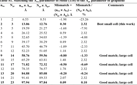
The smallest-size cell with small lattice mismatch (2.32% and 1.44% in the A and B directions, respectively), is the combination of a 36 supercell of graphene with a 25 supercell of rutile (110),
1 J. K. Burdett, T. Hughbanks, G. J. Miller, J. W. Richardson, J. V. Smith, J. Am. Chem. Soc. 1987, 109, 3639–
[image:3.595.152.435.391.483.2]S3
[image:4.595.75.515.164.439.2]used in this work (192 atoms when the 6 atomic-layer rutile slab is used, or 252 atoms with the 9 atomic-layer rutile slab) and in the literature.2 Mismatch below 2% can be achieved only with much larger cell sizes involving over 1000 atoms (Table S3). This much greater computational expense is not expected to greatly improve the accuracy of the interface model (see strain tests, Fig. 2 in the main text and Table S7).
Table S1. Matching the Aru parameter of rutile (110) to the Agr parameter of graphene nru Ngr nru Aru,
Å
Ngr Agr, Å
Mismatch = (nru Aru) – (Ngr Agr), Å
Mismatch / (Ngr Agr),
%
Comments
1 2 6.53 8.51 -1.98 -23.26
2 3 13.06 12.76 0.30 2.32 Best small cell (this work)
3 5 19.59 21.27 -1.68 -7.91
4 6 26.12 25.52 0.59 2.32
5 8 32.65 34.03 -1.39 -4.08
6 9 39.17 38.29 0.89 2.32
7 11 45.70 46.79 -1.09 -2.33
8 12 52.23 51.05 1.18 2.32
9 14 58.76 59.56 -0.80 -1.33 Good match; large cell
10 15 65.29 63.81 1.48 2.32
11 17 71.82 72.32 -0.50 -0.69 Good match; large cell
12 18 78.35 76.57 1.78 2.32
13 20 84.88 85.08 -0.20 -0.24 Good match; large cell
14 21 91.41 89.33 2.07 2.32
[image:4.595.74.518.468.732.2]15 23 97.94 97.84 0.09 0.10 Good match; large cell
Table S2. Matching the Bru parameter of rutile (110) to the Bgr parameter of graphene mru Mgr mru Bru,
Å
Mgr Bgr, Å
Mismatch = (mru Bru) – (Mgr Bgr), Å
Mismatch / (Mgr Bgr),
%
Comments
1 1 3.00 2.46 0.54 21.75
2 3 5.99 7.38 -1.39 -18.83
3 4 8.99 9.84 -0.86 -8.69
4 5 11.98 12.30 -0.32 -2.60 Alternative smaller cell
5 6 14.98 14.76 0.22 1.46 Best small cell (this work)
6 7 17.97 17.22 0.75 4.36
7 9 20.97 22.14 -1.18 -5.31
8 10 23.96 24.60 -0.64 -2.60
9 11 26.96 27.06 -0.10 -0.39 Good match; large cell
10 12 29.95 29.52 0.43 1.46
11 13 32.95 31.98 0.97 3.02
12 15 35.94 36.90 -0.96 -2.60 13 16 38.94 39.36 -0.42 -1.08
14 17 41.93 41.82 0.11 0.26 Good match; large cell
15 18 44.93 44.28 0.65 1.46
2
S4
Table S3. Sizes of rutile (110)/graphene composite cells with small lattice mismatch: nru mru rutile (110) cells interfaced with Ngr Mgr graphene cells
nru mru Ngr Mgr Number of atoms (with 6 atomic-layer
TiO2)
Number of atoms (with 9 atomic-layer
TiO2)
Mismatch along A and B, %
2 5 3 6 192 252 +2.32% and +1.46%
2 9 3 11 348 456 +2.32% and -0.39%
2 14 3 14 540 708 +2.32% and +0.26%
9 14 3 6 876 1146 -1.33% and +1.46%
9 14 3 11 1588 2074 -1.33% and -0.39%
9 14 3 14 2464 3220 -1.33% and +0.26%
15 23 3 6 1212 1662 +0.10% and +1.46%
15 23 3 11 2192 3002 +0.10% and -0.39% 15 23 3 14 3404 4664 +0.10% and +0.26%
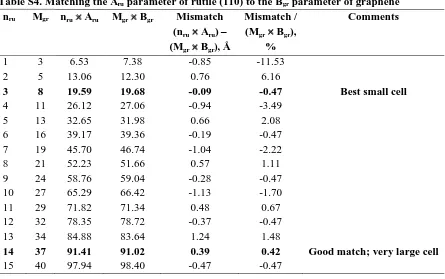
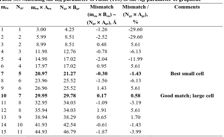
(ii) Tables S4 and S5 describe the lattice matching procedure for case (ii), i.e. the orientation of graphene with respect to rutile (110) where the zigzag line of graphene (vector Bgr) runs parallel to the Aru cell vector of rutile (110), shown in Figure S1. Here, combinations of nru, Mgr, mru, Agr should ensure nru Aru = Mgr Bgr, and mru Bru = Ngr Agr. We find that commensurability of nru Aru with Mgr Bgr can be achieved already with small supercell extensions, while commensurability of mru Bru with Ngr Agr requires large supercell extensions.
Cell sizes for the resulting best composite cells are given in Table S6. The smallest commensurate unit cell combines an 8 5 supercell of graphene with a 3 7 supercell of rutile (110), with the strain of -1.43% and -0.47% to the armchair and zigzag graphene directions, respectively (412 atoms with a 6 atomic layer slab of rutile (110)). An even better match (strain of -0.47% and +0.58% in the armchair and zigzag lines, respectively) can be obtained by combining an 87 supercell of graphene with a 310 supercell of rutile (110), but the cell size (584 atoms with a 6 atomic layer rutile (110) slab) is too large for practical use, and improvements in quality are expected to be minimal.
Table S4. Matching the Aru parameter of rutile (110) to the Bgr parameter of graphene nru Mgr nru Aru Mgr Bgr Mismatch
(nru Aru) – (Mgr Bgr), Å
Mismatch / (Mgr Bgr),
%
Comments
1 3 6.53 7.38 -0.85 -11.53
2 5 13.06 12.30 0.76 6.16
3 8 19.59 19.68 -0.09 -0.47 Best small cell
4 11 26.12 27.06 -0.94 -3.49
5 13 32.65 31.98 0.66 2.08
6 16 39.17 39.36 -0.19 -0.47 7 19 45.70 46.74 -1.04 -2.22
8 21 52.23 51.66 0.57 1.11
9 24 58.76 59.04 -0.28 -0.47 10 27 65.29 66.42 -1.13 -1.70 11 29 71.82 71.34 0.48 0.67 12 32 78.35 78.72 -0.37 -0.47 13 34 84.88 83.64 1.24 1.48
14 37 91.41 91.02 0.39 0.42 Good match; very large cell
[image:5.595.74.519.501.780.2]S5
Table S5. Matching the Bru parameter of rutile (110) to the Agr parameter of graphene mru Ngr mru Aru Ngr Bgr Mismatch
(mru Bru) – (Ngr Agr), Å
Mismatch / (Ngr Agr),
%
Comments
1 1 3.00 4.25 -1.26 -29.60
2 2 5.99 8.51 -2.52 -29.60
3 2 8.99 8.51 0.48 5.61
4 3 11.98 12.76 -0.78 -6.13
5 4 14.98 17.02 -2.04 -11.99
6 4 17.97 17.02 0.95 5.61
7 5 20.97 21.27 -0.30 -1.43 Best small cell
8 6 23.96 25.52 -1.56 -6.13
9 6 26.96 25.52 1.43 5.61
10 7 29.95 29.78 0.17 0.58 Good match; large cell
11 8 32.95 34.03 -1.09 -3.19
12 8 35.94 34.03 1.91 5.61
13 9 38.94 38.29 0.65 1.70
14 10 41.93 42.54 -0.61 -1.43 15 11 44.93 46.79 -1.87 -3.99
Table S6. Sizes of rutile (110)/graphene composite cells with small lattice mismatch: nru mru rutile (110) cells interfaced with Mgr Ngr graphene cells: graphene’s zigzag direction (Mgr Bgr) is parallel to the nru Aru cell vector of rutile (110)
nru mru Mgr Ngr Number of atoms (with 6 atomic-layer
TiO2)
Number of atoms (with 9 atomic-layer
TiO2)
Mismatch along Aru and Bru, %
3 7 8 5 412 538 -0.47% and -1.43%
3 10 8 7 584 764 -0.47% and +0.57%
14 7 8 5 2504 3386 +0.42% and -1.43%
[image:6.595.72.524.427.534.2]S6
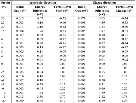
[image:7.595.73.525.142.487.2]S2. Strain tests data: band gaps, energies and Fermi level shifts
Table S7. Change in observed band gap, Fermi level and total energy difference relative to fully optimised orthorhombic graphene for each level of applied strain. These data are also presented graphically in Figure 3 of the main text
Strain Armchair direction Zigzag direction
(%) Band
Gap (eV)
Energy Difference
(eV)
Fermi Level Shift (eV)
Band Gap (eV)
Energy Difference
(eV)
Fermi Level Change (eV)
30 0.013 4.67 -0.73 0.173 5.63 -0.74
25 0.003 4.16 -0.66 0.003 4.39 -0.53
20 0.011 3.10 -0.42 0.002 3.14 -0.40
15 0.006 1.98 -0.33 0.005 1.97 -0.33
10 0.007 0.99 -0.25 0.006 0.98 -0.25
6 0.011 0.39 -0.17 0.007 0.38 -0.17
5 0.001 0.28 -0.15 0.001 0.27 -0.14
4 0.003 0.19 -0.12 0.008 0.18 -0.12
3 0.005 0.11 -0.09 0.008 0.10 -0.09
2 0.004 0.05 -0.06 0.005 0.05 -0.06
1 0.010 0.01 -0.03 0.004 0.01 -0.02
0 0.001 0.00 0.00 0.001 0.00 0.00
-1 0.007 0.01 0.04 0.007 0.01 0.04
-2 0.005 0.04 0.08 0.002 0.05 0.08
-3 0.010 0.10 0.08 0.008 0.11 0.12
-4 0.002 0.18 0.13 0.001 0.20 0.16
-5 0.003 0.29 0.17 0.006 0.31 0.20
-6 0.008 0.43 0.22 0.008 0.46 0.25
-10 0.001 1.34 0.46 0.001 1.39 0.46
-15 0.013 3.30 0.77 0.006 3.42 0.78
-20 0.009 6.39 1.12 0.008 6.59 1.28
The accuracy of our estimated band gaps is limited by the density of the k-point sampling. We evaluate the uncertainly in our band gaps as 0.01 eV (as the difference between the conduction band energies at the Dirac point and at the next k-point). This uncertainty is similar to those reported in earlier studies: 0.01 eV3 or 0.0003-0.04 eV depending in the k-point grid4.
3 N. Kerszberg, P. Suryanarayana. RSC Adv. 2015, 5, 43810–43814. 4
S7
S3. Band structures of highly strained graphene
Figure S2 displays the band structures of graphene unit cells under 20, 25, and 30% applied tensile uniaxial strain in the armchair and zigzag directions. The band gaps reported in the main article (Figure 2) and below in Table S7 are obtained from the band structures and are defined as the energy gaps between the highest fully or partially-occupied electronic band and the lowest unoccupied band. In the case of structures D and F of Figure S2 one can see that here the Fermi level is not at the Dirac point, and thus the highest-occupied band is only partially occupied.
Figure S2. Band structures of highly-strained graphene unit cells: 20% armchair (A) and zigzag
[image:8.595.74.522.183.599.2]S8
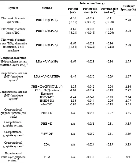
S4. Interaction energies in the TiO
2/graphene system
Table S8. Interlayer interaction energies (with binding energies in brackets) and interlayer spacings obtained in this work and in several published systems (see references).
System Method
Interaction Energy
Interlayer Spacing (Å) Per cell
(eV) Per carbon atom (eV) Per unit area (mJ m-2) This work, 6 atomic
layers TiO2 PBE + D (CP2K) (--1.352.40)
-0.019
(-0.033)
-0.11
(-0.20) 2.90
This work, 9 atomic
layers TiO2 PBE + D (CP2K) (--1.673.24)
-0.023
(-0.045)
-0.14
(-0.26) 2.76
This work, 6 atomic layers TiO2, alternative
orientation, 8 x 5 graphene
PBE + D (CP2K) (--3.674.55) (--0.0230.028) (--0.140.18) 2.90
Computational rutile (110)/graphene system
(9 atomic layers TiO2)2 LDA + U (VASP) -1.69 -0.023 -0.14 2.75
Computational anatase (101)/graphene
system5 LDA + U (CASTEP)
-1.49 -0.050 -0.29 2.57
Computational anatase (101)/graphene
system6
PBE + D (CRYSTAL 14) PBE + D (Quantum
Espresso) B3LYP-D*
HSE06-D2
vdw-DF2
-1.25 -1.01 -1.44 -1.33 -0.95 -0.042 -0.034 -0.048 -0.044 -0.032 -0.24 -0.19 -0.28 -0.26 -0.18 2.84 2.97 2.84 2.77 3.05 Computational
graphite system (this
work) PBE + D n/a -0.044 -0.27 3.35
Computational
graphite system7 PBE + D n/a -0.051 -0.31 3.35 Computational
graphite system8 VdW-DF n/a -0.050 -0.31 3.59
Computational
graphite system9 LDA n/a -0.024 -0.15 3.33
Experimental multilayer graphene
system10 TEM n/a
-0.035 -0.21 n/a
5 X. Li, H. Gao and G. Liu, Computational and Theoretical Chemistry, 2013, 1025, 30-34. 6 L. Ferrighi, G. Fazio and C. Di Valentin, Adv. Mater. Interf., 2016, 3, 1500624.
7
I. V. Lebedeva, A. A. Knizhnik, A. M. Popov, Y. E. Lozovik and B. V. Potapkin, Phys. Chem. Chem. Phys., 2011, 13, 5687-95.
8 E. Ziambaras, J. Kleis, E. Schröder and P. Hyldgaard, Phys. Rev. B, 2007, 76, 155425.
[image:9.595.78.526.127.669.2]S9
S5. Density of states for the 6-atomic-layer rutile (110)/graphene
composite system
Figure S3 shows the projected density of states (PDoS) data for the 6-atomic-layer rutile (110) slab with and without the presence of graphene. Unlike the 9-atomic-layer composite system (Figure 5 in the main text), there is no significant interaction in the TiO2 forbidden region between graphene and rutile (110), nor any shift in the positions of the titanium bands above the conduction band of TiO2. The only noteworthy change in the structure is the appearance of carbon bands in the band gap of TiO2.
Figure S3. PDoS plot of the 6-atomic-layer rutile (110) slab (bottom) and its composite with
[image:10.595.77.504.214.474.2]S10
S6. Charge density difference in the rutile (110)/graphene composite
system
Figure S4 shows the spatial charge density difference between the composite systems and the isolated TiO2 and graphene systems, for our two TiO2 slab sizes. In both cases there is a pattern of charge migration across the interface from graphene to rutile, with the magnitude of charge transfer across the interface (0.01 electrons per carbon atom) comparable to what has been seen in similar studies using DFT+U methods (0.007-0.03 electrons per C atom).2,5,11 Additional evidence for charge transfer from graphene to rutile is seen in the positioning of the Fermi level (Figures 6-7 in the main text), as it lies below the Dirac point by almost 0.5 eV, which is slightly less than that observed in the previous calculations of this interface.2,5 Both our work and the previous research clearly show that some spontaneous charge transfer from graphene to rutile occurs upon formation of this composite system.
Figure S4. Spatial charge density differences in composites containing the 9 atomic layer (top)
and 6 atomic layer (bottom) rutile (110), at isosurface values of 10-3 electrons Bohr-3.
11
[image:11.595.137.457.273.557.2]S11
S7. Band structures of the rutile (110) and graphene components
Figure S5 shows the band structures of the isolated graphene and the 9-atomic-layer rutile (110) components of the TiO2/graphene composite. The band structures for the components of the composite show the same characteristic shape as parts the combined composite, such as the flat TiO2 bands and the more dispersed graphene bands, with the Dirac point appearing away from the point. Comparing the two band structures with the full composite (Figure 7 in the main text) shows that there is little change to the band structure upon formation of the composite.
Figure S5. Band structures of the graphene (top) and the 9-atomic-layer rutile (110) (bottom)
[image:12.595.137.461.182.510.2]S12
S8. Example of CP2K input file for rutile (110)/graphene system
Listed here are the input settings used in the geometry optimisation of the 9 atomic layer rutile (110)/graphene composite unit cell, using the HSE06 hybrid functional with the CP2K software package, as described in the main article. Special care must be taken with the value of
EPS_SCHWARZ (which defines the integral screening parameter) when incorporating graphene in the
calculation, as this number needs to be sufficiently small to prevent numerical instabilities from causing the SCF procedure to fail. Smaller values will increase the number of integrals used in the calculation of Hartree-Fock exchange, but subsequently raise the demand on computing resources. Smaller basis sets are typically better conditioned, and thus do not need such a small value of
EPS_SCHWARZ to avoid convergence issues.
&GLOBAL
PROJECT Rutile-110-Graphene-Unit-HSE06-3layer RUN_TYPE GEO_OPT
PRINT_LEVEL LOW &END GLOBAL
&MOTION &GEO_OPT OPTIMIZER CG &CG
&END CG &END GEO_OPT &END MOTION
&FORCE_EVAL
METHOD Quickstep &DFT
WFN_RESTART_FILE_NAME Rutile-110-Graphene-Unit-HSE06-3layer-RESTART.wfn
&AUXILIARY_DENSITY_MATRIX_METHOD &END AUXILIARY_DENSITY_MATRIX_METHOD &MGRID
CUTOFF 600 NGRIDS 5 &END MGRID &QS
EPS_PGF_ORB 1.0E-20 &END QS
&SCF
SCF_GUESS RESTART EPS_SCF 1.0E-6 MAX_SCF 51 &OT
MINIMIZER CG
PRECONDITIONER FULL_SINGLE_INVERSE ENERGY_GAP 0.1
&END OT &OUTER_SCF
EPS_SCF 1.0E-6 MAX_SCF 20 &END OUTER_SCF &END SCF
&XC
S13 &PBE SCALE_X 0.0 SCALE_C 1.0 &END PBE &XWPBE SCALE_X -0.25 SCALE_X0 1.0 OMEGA 0.11 &END XWPBE &END XC_FUNCTIONAL &HF FRACTION 0.25 &SCREENING EPS_SCHWARZ 1.0E-7 &END SCREENING &INTERACTION_POTENTIAL POTENTIAL_TYPE SHORTRANGE OMEGA 0.11 &END INTERACTION_POTENTIAL &MEMORY MAX_MEMORY 4000 EPS_STORAGE_SCALING 0.1 &END MEMORY &END HF &VDW_POTENTIAL DISPERSION_FUNCTIONAL PAIR_POTENTIAL &PAIR_POTENTIAL TYPE DFTD2 REFERENCE_FUNCTIONAL PBE &END PAIR_POTENTIAL &END VDW_POTENTIAL &END XC &END DFT &SUBSYS &KIND O BASIS_SET DZVP-MOLOPT-GTH-q6 POTENTIAL GTH-PBE-q6 AUX_FIT_BASIS_SET FIT3 &END KIND &KIND Ti BASIS_SET DZVP-MOLOPT-SR-GTH-q12 POTENTIAL GTH-PBE-q12 AUX_FIT_BASIS_SET FIT11 &END KIND &KIND C BASIS_SET DZVP-MOLOPT-GTH-q4 POTENTIAL GTH-PBE-q4 AUX_FIT_BASIS_SET FIT3 &END KIND &CELL