Rochester Institute of Technology
RIT Scholar Works
Theses Thesis/Dissertation Collections
2012
A Silicon p-i-n detector for a hybrid CMOS
imaging system
Christopher Shea
Follow this and additional works at:http://scholarworks.rit.edu/theses
This Thesis is brought to you for free and open access by the Thesis/Dissertation Collections at RIT Scholar Works. It has been accepted for inclusion in Theses by an authorized administrator of RIT Scholar Works. For more information, please contactritscholarworks@rit.edu.
Recommended Citation
i
Title Page
A Silicon p-i-n Detector for a Hybrid CMOS Imaging System
Christopher G. Shea
A Thesis Submitted
In Partial Fulfillment
of the Requirements of the Degree of
Master of Science
in Microelectronic Engineering
Approved by:
Professor ______________________________________
Dr. Karl D. Hirschman (Thesis Advisor)
Professor ______________________________________
Dr. Alan Raisanen (Thesis Committee Member)
Professor ______________________________________
Dr. Donald Figer (Thesis Committee Member)
Professor ______________________________________
Dr. Michael Jackson (Thesis Committee Member)
Professor ______________________________________
Dr. Robert Pearson (Program Director)
Professor ______________________________________
Dr. Sohail Dianat (Deparment Head)
DEPARTMENT OF ELECTRICAL AND MICROELECTRONIC ENGINEERING
COLLEGE OF ENGINEERING
ROCHESTER INSTITUTE OF TECHNOLOGY
ROCHESTER, NEW YORK
ii
Acknowledgment
I would like to thank Dr. Karl D. Hirschman for his steadfast support and
continual guidance throughout my collegiate experience. After first taking me on as a
student researcher, and then continuing as an advisor on both my senior design and thesis
projects, I am eternally grateful to Dr. Hirschman for his support of my academic career.
I would like to thank Dr. Don Figer for entrusting me with the completion of p-i-n image
sensor project. Al Raisanen, Brian Ashe and Nancy Stoffel are all greatly appreciated for
their support and advice throughout the project. I am grateful to have been surrounded by
a bright class of graduate students to provide stimulating discussion and companionship
throughout the long nights in the cleanroom. I would also like to specifically thank
Jon-Paul DesOrmeaux for his continued moral, emotional, physical, social, and psychological
support as only a true friend can provide, and especially my mother for none of this
would be possible without her eternal love and support.
Support for this project is provided by the National Aeronautics and Space
Administration (NASA) under Grant NNX07AG99G, issued through the Astronomy and
Physics Research and Analysis (APRA) Program of the Science Mission Directorate to
iii
Technology (RIT). All simulations were performed in the Very Large Scale Integration
(VLSI) Laboratory and all device fabrication was completed in the Semiconductor &
Microsystems Fabrication Laboratory (SMFL), both at RIT. All photo-masks for the
project were written in house at the SMFL, thanks to Mr. Thomas Grimsley.
Deposition of indium as the bump bond metal was performed at Jet Process
Corporation (JPC) in North Haven, CT using the jet deposition process. Lift-off and
flip-chip bonding were performed at Smart System Technology & Commercialization Center
iv
Abstract
A fully depleted silicon p-i-n image sensor for a very low noise hybrid CMOS
imaging system was simulated, fabricated, and electrically characterized. The image
sensor was then bonded to the foundry fabricated CMOS circuitry to create the imaging
system. SILVACO Atlas was used to simulate the steady state electrical operation of the
device as well as the optical response. Revisions were made to an existing mask set to
allow the use of both contact and projection lithography in the fabrication process.
Significant process improvements were introduced to eliminate needless complexity and
reduce leakage current from the previously reported 1.5x10⁻⁶ A/cm2 below the goal of
2.2x10⁻⁹ A/cm2. Following fabrication of the image sensors, electrical testing was
performed to verify diode quality from leakage and lifetime measurements. A lift-off
process was developed for thick metal layers used in the bump-bond hybridization
process. Daisy-chain test parts were created to characterize the mechanical and electrical
connections formed in the hybridization process. Fabricated p-i-n photodiode arrays
were diced and hybridized to read-out integrated circuits using a flip-chip bump bond
v
Table of Contents
Title Page ...i
Acknowledgment ... ii
Abstract ...iv
Table of Contents ... v
List of Tables ... viii
List of Figures ...ix
1. Introduction ... 1
1.1. A Review of Photodetectors ... 2
1.2. A Historical Perspective ... 3
1.3. Detector Materials ... 4
1.4. Image Sensor Architectures... 6
1.4.1 CCD and CMOS Pixel Architectures ... 7
1.4.2 System Architecture: Hybrid vs. Monolithic ... 9
1.4.3 Hybrid Image Detectors... 12
1.5. APRA Imaging System ... 13
1.5.1 APRA Hybrid Imaging System ... 14
1.5.2 MOSIS Read-out Integrated Circuit (ROIC) ... 16
1.5.3 Silicon p-i-n Photodiode Array ... 17
2. p-i-n Photodiode Operation ... 20
2.1. Junction Electrostatics ... 20
2.1.1 Current-Voltage Characteristics ... 22
2.1.2 Minority Carrier Lifetime ... 26
2.1.3 Open-Circuit Voltage Decay (OCVD) Method ... 27
2.1.4 Reverse Recovery Method... 28
2.2. Absorption and Photogeneration ... 29
2.3. Illuminated Operation ... 33
2.3.1 Charge Collection ... 34
2.3.2 Quantum Efficiency ... 35
2.3.3 Point Spread Function ... 35
3. SILVACO Atlas TCAD Simulations ... 37
3.1. Numerical Poisson Solver Theory ... 37
vi
3.1.2 Continuity Equations ... 38
3.1.3 Drift-Diffusion Transport Equations ... 39
3.2. Atlas Simulation Organization ... 39
3.2.1 Device Structure Specification ... 41
3.2.2 Material Models... 44
3.2.3 Numerical Methods ... 48
3.2.4 Solutions Specification ... 50
3.3. Simulation Results... 52
3.3.1 Current Voltage Characteristics ... 52
3.3.2 Quantum Efficiency ... 56
3.3.3 Point Spread Function ... 64
4. Layout and Fabrication ... 70
4.1. Existing Layout ... 70
4.2. Mask Design ... 71
4.2.1 Revised Test Die... 72
4.3. Process Flow ... 73
4.3.1 Front–to–Backside Alignment ... 75
4.3.2 Contact Cut Etch... 78
4.3.3 Aluminum Dry Etch ... 80
5. Electrical Testing ... 84
5.1. Previous Results ... 84
5.2. Current-Voltage Characteristics ... 86
5.2.1 On-State Ideality ... 87
5.2.2 Off-State Leakage ... 89
5.3. Junction Lifetime Measurements ... 93
5.4. Spectral Response Measurements ... 95
6. Hybridization ... 96
6.1. Lift-Off Process Development ... 97
6.1.1 Previous Development Work ... 99
6.1.2 Initial Investigation ... 102
6.1.3 SC 1827 on LOR-30A Development ... 104
6.1.4 Indium Deposition ... 106
6.1.5 SC 1827 on Double-Coat LOR-30A... 108
6.2. ROIC Passivation Cut ... 110
6.3. Bump-Bond Daisy Chain Test Parts ... 113
vii
6.3.2 Electrical Testing ... 118
6.4. Final Hybridized Devices ... 119
7. Final Remarks ... 121
Appendix I Typical Atlas Input File ... 123
Appendix II Process Flow ... 125
viii
List of Tables
TABLE 1SUMMARY COMPARISON OF CCD AND CMOS TECHNOLOGIES [8] ... 8
TABLE 2IMAGING SYSTEM PERFORMANCE GOALS [14] ... 14
ix
List of Figures
Fig. 1.1 Data showing a) number of pixels and b) pixel area for imaging sensors reported in IEEE
publications [3]... 4
Fig. 1.2 Optical absorption coefficients for various semiconductor materials [4] ... 5
Fig. 1.3 Schematic representation of CCD and CMOS image sensors highlighting the differences of operation taken from [7] ... 8
Fig. 1.4 Typical monolithic CMOS image sensor [11] ... 10
Fig. 1.5 Schematic representation of front-side illumination (FSI) vs back-side illumination (BSI) [12] ... 11
Fig. 1.6 Cross-section of hybrid imager used in ATLAS detector [13] ... 13
Fig. 1.8 Illustration of Hybridized Image Detector cross-section ... 15
Fig. 1.9 Top Down Illustration of Hybridized Image Detector ... 16
Fig. 1.10 Optical Micrograph of ROIC die ... 17
Fig. 1.11 Pixel Design and Layout ... 17
Fig. 1.12 Layout of 256x128 p-i-n photodiode array with guard ring ... 18
Fig. 2.1 Current-voltage characteristics of a practical Si diode showing ideal and experimental behavior in forward and reverse modes of operation [4] ... 22
Fig. 2.2 Lifetime (τp) and Diffusion length (Lp) of Holes in n-type Si as a function of Donor density [17] ... 25
Fig. 2.3 Current and voltage transients observed in the methods used for carrier ... 27
Fig. 2.4 Complex refractive index vs. wavelength for silicon ... 29
x
Fig. 2.6 Absorption coefficient and penetration depth vs. wavelength for silicon ... 31
Fig. 3.1 Atlas Input Code Organizational Structure ... 39
Fig. 3.2 Atlas example mesh definition code ... 41
Fig. 3.3 Atlas simulation code defining electrode name as positions and doping profiles ... 42
Fig. 3.4 Atlas code defining material and interface properties and specifying numerical models ... 43
Fig. 3.5 Flow diagram for Newton method [24]... 47
Fig. 3.6 Atlas specification of solution method and parameters ... 48
Fig. 3.7 Atlas solution specification code sample ... 49
Fig. 3.8 Simulated p-i-n diode forward bias current density ... 53
Fig. 3.9 Simulated p-i-n diode reverse bias leakage current vs. applied bias ... 54
Fig. 3.10 Simulated reverse bias current density at 50 V vs. minority carrier lifetime ... 55
Fig. 3.11 Typical quantum efficiency curve from SILVACO Atlas ... 56
Fig. 3.12 QE curves for surface grid resolution from 0.001 to 0.1 µm ... 57
Fig. 3.13 Simulated QE curves for surface dopant concentrations ranging from 1x1017 cm-3 to 1x1021 cm-3 ... 58
Fig. 3.14 Simulated QE curves for n+ – n– homo-junction depths of 0.3 – 1.0 µm ... 59
Fig. 3.15 Dopant and electron concentration profiles on n-type light absorbing side ... 60
Fig. 3.16 Simulated QE curves for operating biases from 1 to 100 V ... 61
Fig. 3.17 QE curves for detector thicknesses from 10 to 300 µm ... 62
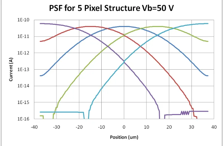
Fig. 3.18 Point spread function simulations showing current through pixels as a function of the source illumination position ... 63
xi
Fig. 3.20 Simulated current vs. illumination position for 50, 75, 100, 125 & 150 V ... 65
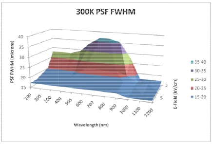
Fig. 3.21 FWHM of Simulated PSF for 100 – 1200 nm and 2 – 6 kV/cm at 300 K ... 66
Fig. 3.22 Full width half max of point spread function vs. wavelength at 2 kV/cm for 200 K and 300 K ... 67
Fig. 3.23 Simulated hole concentration distributions for centered point source illumination at 50 V reverse bias and 300 K for various wavelengths in 5 pixel structure ... 68
Fig. 4.1 CAD rendering of contact lithography mask layout of (a) entire wafer and (b) close-up of test structures ... 70
Fig. 4.2 CAD renderings of (a) projection die and (b) contact mask layout ... 71
Fig. 4.3 CAD renderings of (a) Process characterization test die and (b) Pixel characterization test die ... 72
Fig. 4.4 Summary of key steps in revised process flow ... 73
Fig. 4.5 Comparison of current and newly developed front-to-back side alignment process ... 75
Fig. 4.6 Optical Micrographs of Metal layer pattern after (a) contact lithography (b) projection lithography ... 77
Fig. 4.7 An optical micrograph of the array after contact cut etch where the failure mechanism can be observed ... 78
Fig. 4.8 Optical mirograph of features in LOR layer exhibiting blow-out and scumming ... 79
Fig. 4.9 Patterned aluminum layer on bump bond side of device showing thin grid lines due to undercutting during wet etch process ... 80
Fig. 4.10 Resolution features etched into aluminum layer using suggested recipe. Note significant undercut of resist features ... 81
Fig. 4.11 Patterned aluminum pixel contacts dry etched with optimized recipe ... 82
Fig. 5.1 Representative current-voltage characteristics of p-i-n diode fabricated by Kolb with ideality fits [26] ... 84
xii
Fig. 5.3 Measured forward bias I-V characteristics of rev3 p-i-n diode with exponential fits and
resulting ideality factors ... 86
Fig. 5.4 Forward bias I-V characteristics of 25X p-i-n diode measured from 255 K to 300 K showing temperature dependence ... 87
Fig. 5.5 Overlay of reverse bias leakage currents from best wafer of the final two processing runs ... 88
Fig. 5.6 Wafer map of leakage current uniformity for final two processing run. ... 89
Fig. 5.7 Measure reverse bias leakage current vs. applied potential from 260 to 350 K ... 90
Fig. 5.8 Reverse bias leakage current density at 50 V from 250 to 350 K with exponential extrapolation down to 200 K ... 91
Fig. 5.9 Diode junction voltage decay with exponential fit ... 93
Fig. 5.10 Short circuit spectral response of p-i-n diode ... 94
Fig. 6.1 Schematic representation of lift-off and flip chip bump bonding technique used for hybridization process ... 96
Fig. 6.2 Scanning electron micrograph of bump bond opening in bi-layer resist stack of HPR504 on LOR-30A [26] ... 99
Fig. 6.3 SEM cross-section of bump-bonds after deposition of (a) gold-tin (b) indium ... 100
Fig. 6.4 SEM of bump-bond array after lift-off (a) gold-tin(b) indium ... 101
Fig. 6.5 SEM cross-section of resist profile after development for various processes ... 102
Fig. 6.6 SEM cross-section and correlating optical micrograph of bump-bond ... 104
Fig. 6.7 SEM of new thick bi-layer LOR process after deposition of 3 µm of indium ... 105
Fig. 6.8 SEM of several 3 µm tall indium bumps after lift-off of excess material ... 106
Fig. 6.9 SEM of bi-layer resist process with two LOR layers ... 107
Fig. 6.10 SEM of thick bi-layer resist process after 4.6 µm of indium deposition ... 108
xiii
Fig. 6.12 SEM cross-section of ROIC die through etched bond pad... 112
Fig. 6.13 Screen capture of bump-bond daisy chain ROIC test part VLSI layout... 114
Fig. 6.14 Infra-red optical micrograph of the corner of the bump bond array ... 116
Fig. 6.15 Optical micrograph of 5 µm thick indium bumps after bonding and separation ... 116
Fig. 6.16 SEM of 1 µm indium bump after bonding and separation ... 117
Fig. 6.17 Measured resistance of columns of 84 bump bonds ... 118
1
Chapter 1
1.
Introduction
The 2009 Nobel Prize in Physics was awarded to Willard S. Boyle and George E.
Smith from Bell Labs for their 1969 invention of the charge-coupled device (CCD), a
solid state image sensor that has led to many scientific discoveries and consumer
applications. Image sensor technology has evolved dramatically throughout the years,
introducing new technologies such as active pixels, complimentary
metal-oxide-semiconductor (CMOS) image sensors and more recently the hybrid detector [1-8].
An imaging system contains several key components, including a photodetector,
read-out circuitry, and a collection of optical elements. The photodetector is a transducer
designed to convert an optical signal into an electrical signal. The material must have
desirable electrical properties that can be modified by an optical signal. Semiconductors
are perfectly suited to this task due to the profound effect electromagnetic radiation has
on the material. The read-out circuitry accesses many different elements of a large array
and conditions the signal for output. The optical system is responsible for collecting the
light in the desired field of view, and focusing this light onto the image sensor, or focal
2
Image sensors have become an invaluable tool to astronomical research enabling
the discovery of new phenomena and the confirmation of models. Imaging systems
operating in the harsh environments of outer space must be able to perform at cryogenic
temperatures and withstand high energy radiation. This thesis continued the development
of a fully depleted silicon p-i-n image sensor and hybridization process for a hybrid
CMOS focal plane array enabling future NASA space missions.
1.1.A Review of Photodetectors
There are several types of semiconductor based photodetectors including
photoconductors, photodiodes, charge-coupled devices, and phototransistors. The
devices are classified by their structure and the principles upon which they operate. In a
photoconductor a single piece of homogeneous semiconducting material is contacted by
ohmic connections and the resistivity is modulated by the optical signal. Photodiodes
consist of a metallurgical junction in a semiconducting material that is reverse biased to
sweep out photo-generated carriers to the collection terminals. Charge-coupled devices
are a special type of detector where an array of gated capacitors is incorporated to collect
photogenerated carriers. These carriers are then transferred to the edge of the device and
3
an optical signal to modulate gain of the transistor. Each device has advantages and
disadvantages associated with the design and are suited to different applications.
A silicon p-i-n photodiode is similar to the ubiquitous p-n diode, except a nearly
intrinsic region exists between the two highly doped terminals. In the reverse bias mode
of operation, the entire intrinsic region is typically depleted providing a large volume for
the photogeneration of carriers. One of the main advantages of the p-i-n photodiode is
the thickness of the depleted intrinsic region can be tailored to optimize absorption at a
desired wavelength. The absence of impurities in the depleted region and the use of high
quality float zone silicon allow devices with extremely low leakage levels to be realized.
1.2.A Historical Perspective
Image sensors have developed very rapidly over the past five decades, helped
enormously by the vast amount of research performed by the semiconductor industry.
Using processes developed for integrated circuit manufacturing the image sensor industry
has been able to shrink pixel size and increase total pixel counts at rates comparable to
transistors in the IC industry. Luppino and Burke even created their own version of
‘Moore’s Law’ stating pixel count and density would double every 2.5 years [2]. A
graphical illustration of the trends can be seen in Fig. 1.1 a) and b) showing the pixel
4
a) b)
Fig. 1.1 Data showing a) number of pixels and b) pixel area for imaging sensors reported
in IEEE publications [3]
Like Moore’s Law, this trend will eventually be faced by fundamental limitations
restricting further growth. The number of pixels in a device is limited by the size of each
pixel and the substrates used for manufacturing. Currently, most high grade scientific
imagers are produced on 150 mm substrates, leaving the industry room for growth up to
the current IC industry standard of 300 mm. The large areas required by the detectors
however make defect densities a primary concern. The size of individual pixels is limited
by the volume of detecting material required to produce a suitable signal for the sensing
circuitry. The ability to prevent bleeding of a signal into adjacent pixels also limits the
reduction of pixel area and becomes more difficult with increasing detector thickness.
1.3.Detector Materials
There are many different semiconducting materials that can be used as
5
types of radiation a material absorbs and how strongly it does so as shown by the
absorption coefficient. An excellent illustration of the optical properties of various
[image:19.612.113.535.199.608.2]semiconductor materials shown in Fig. 1.2 is taken from Sze.
Fig. 1.2 Optical absorption coefficients for various semiconductor materials [4]
Silicon can be seen to absorb light at a reasonable rate (102 – 104 cm-1) over a
6
attractive material. Although germanium has an even higher absorption over a wider
range of wavelengths, it has several drawbacks that limit its applications. The rarity of
the material makes it considerably more expensive, and a smaller band gap creates much
higher thermally generated noise. All work in this project was completed on ultra-high
purity float zone silicon substrates. Float zone substrates are produced by passing an RF
induction coil over a poly-Si rod, melting the material and inducing a single crystal
growth. The absence of a crucible or any direct contact with melted Si, as found in
traditional Czochralski grown substrates, reduces the introduction of carbon and oxygen
impurities. The lower oxygen levels eliminate the need to form an oxygen depleted
(denuded) zone resulting in consistent material properties throughout the thickness of the
wafer.
1.4.Image Sensor Architectures
Image sensors can be classified based on the architecture at either the system level
or the pixel level. The two types of system level architecture are monolithic and hybrid.
A monolithically integrated image sensor contains both the active photodetector region
and all circuitry necessary to convert the charge to a signal conditioned for output on a
single substrate. In hybrid image detectors the active sensing region and readout circuitry
7
connections between the two substrates. Hybrid detectors allow the substrate and
fabrication processes for the image sensor and read out circuitry to be optimized
separately, enabling ultra-low noise imaging systems that are highly sensitive and
radiation hardened. The two types of pixel architecture are CCD and CMOS. The CCD
is a more mature technology and the typical choice for most high end applications,
although CMOS devices are steadily gaining market share.
1.4.1 CCD and CMOS Pixel Architectures
Charge-transfer devices were originally conceived as shift register devices [5], but
their applications to image detection were readily apparent [6]. The main difference
between the two architectures is the method of addressing the collected charge as shown
in Fig. 1.3. In CCD’s, overlapping gate structures serve to shift the charge to the edge of
the array where it is read out, however in CMOS devices each pixel contains at least one
transistor as an access device. Complex devices include additional transistors to amplify
the signal and reduce noise. The use of CMOS processing also greatly eases process
8
Fig. 1.3 Schematic representation of CCD and CMOS image sensors highlighting the
differences of operation taken from [7]
Both architectures have their advantages and disadvantages. A summary of key
aspects of the designs is provided in Table 1 [8]. Historically, CCD’s are known for
delivering a higher quality sensor although at a much higher price. CMOS sensors have
benefited greatly from the advanced processing techniques developed by the memory and
logic sectors making them extremely cost effective.
9
Passive and Active CMOS Pixels
The type of pixel circuitry implemented in a CMOS sensor is an important aspect
of system performance and can be used to categorize the device. The first designs were
passive sensors that utilize a single transistor per pixel as an access device. Active
sensors incorporate per-pixel amplification through the use of source-followers to greatly
increase pixel performance [9]. Additional circuitry can further enhance device
performance by reducing undesirable effects due to device variation and noise, however
the additional transistors occupy precious real estate within the pixel [10]. The
percentage of pixel area available for sensing incoming light is known as the fill factor.
The two most prominent techniques used to mitigate the effects of reduced fill factors are
discussed in the following sections.
1.4.2 System Architecture: Hybrid vs. Monolithic
The first image sensors were monolithically integrated CCD’s based upon the
charge transfer device conceived by Boyle and Smith. In a monolithic device, both the
active sensing region and the read out circuitry are fabricated within the same substrate.
This can require greater process complexity due to the vastly different doping
requirements of the two regions. A top down micrograph of a typical monolithic CMOS
10
surrounded by the logic circuitry used to select the rows and columns and condition the
signal for output.
Fig. 1.4 Typical monolithic CMOS image sensor [11]
Front-side vs. Back-side Illumination
Topography and the use of opaque materials in the fabrication of image sensors
leads to a loss signal before it reaches the photodetector due to absorption, reflection, and
scattering. Transparent conductors such indium-tin-oxide (ITO) are often used to reduce
the need for opaque metals, though imperfect and curved interfaces still cause some
scattering of the light. This reduction of signal is enhanced even further in
multi-transistor pixel designs with decreased fill factors, which are more common than older
Fig. 1.5 Schematic representation of
To eliminate virtually
to flip the substrate over after the processing of front
device from the back. T
fabricated in substrates to
the depleted regions. The devices are
quality backside-surface to avoid the creation of defect sta
and double side polished substrates are used for the creation of these devices. A
reflection layers are also used to almost completely eliminate all reflected light
comparison of front-side illuminated (FSI) and back
shown in Fig. 1.5.
11
Schematic representation of front-side illumination (FSI) vs
back-side illumination (BSI) [12]
virtually all possible sources of external light loss,
over after the processing of front-side is completed and illuminate
This often requires additional processing, as most d
too thick to allow light of sufficient intensities to
. The devices are can be thinned, taking special care to leave a high
surface to avoid the creation of defect states. Often specialty thinned
and double side polished substrates are used for the creation of these devices. A
are also used to almost completely eliminate all reflected light
side illuminated (FSI) and back-side illuminated (BSI) structures is side illumination (FSI) vs
all possible sources of external light loss, one technique is
side is completed and illuminate the
as most devices are
of sufficient intensities to penetrate into
taking special care to leave a high
Often specialty thinned
and double side polished substrates are used for the creation of these devices.
Anti-are also used to almost completely eliminate all reflected light. A
Fig. 1.6
Cross-1.4.3 Hybrid Image Detectors
The development of advanced packaging techniques
hybrid image detectors, where
substrates and then connections are made between the two die
densely spaced interconnections
makes traditional connections
incompatible. A lithographic pattern transfer
processes have enabled large arrays of bumps to be formed with at a very fine pitch.
cross section of the hybr
Hybrid detectors are inherently back
are mated to each other. Wire
12
-section of hybrid imager used in ATLAS detector [
Hybrid Image Detectors
The development of advanced packaging techniques has enabled
, where the sensor and readout circuit are fabricated on separate
ates and then connections are made between the two die. The l
connections between the substrates required for the pixel arrays
traditional connections technologies such as wire-bonding and screen
A lithographic pattern transfer combined with electroplating and lift
processes have enabled large arrays of bumps to be formed with at a very fine pitch.
cross section of the hybrid sensor used in the ATLAS detector is shown in
Hybrid detectors are inherently back-side illuminated as the front-sides of the two chips
are mated to each other. Wire-bond connections are made to the backside of the photo section of hybrid imager used in ATLAS detector [13]
enabled the creation of
the sensor and readout circuit are fabricated on separate
The large matrix of
required for the pixel arrays
bonding and screen-printing
combined with electroplating and lift-off
processes have enabled large arrays of bumps to be formed with at a very fine pitch. A
id sensor used in the ATLAS detector is shown in Fig. 1.6.
sides of the two chips
photo-13
diode to set the operating potential and the periphery of the read-out integrated circuit
(ROIC) for communication.
Another large advantage of hybrid detectors is the ability use different substrates
and fabrication sequences for the sensor and read out circuitry. The read-out circuitry
requires high doping levels for radiation hardness, to prevent latch-up and maintain
proper device operation. The sensor requires low doping levels to reduce leakage
currents and increase the width of the space charge region.
1.5.APRA Imaging System
In 2006, the Rochester Imaging Detector Laboratory (RIDL) at the Rochester
Institute of Technology (RIT) was awarded a grant from the National Aeronautic and
Space Administration (NASA) for “A Very Low Noise CMOS Detector” under the
Astronomy and Physics Research and Analysis (APRA) Program of the Science Mission
Directorate [14]. The stated goal of the project from the grant proposal was “to design,
fabricate, and measure the noise of a novel hybrid CMOS detector with Σ∆ (sigma-delta)
pixel design at cryogenic temperatures.” The initial plan called for the read out circuit to
be fabricated through MOSIS, a low-cost prototyping and small-volume production
service, and the detectors to be fabricated in the Semiconductor and Microsystems
14
1.5.1 APRA Hybrid Imaging System
The APRA Hybrid imaging system was designed as a proof-of-concept device for
astronomical purposes and was expected to meet the performance goals specified Table 2
[14]. A dark current of less than 1 e-/pixel/sec was desired at an operating temperature of
200 K from an 8-12 um pixel. To meet the performance goals, a hybrid architecture was
designed with a silicon CMOS ROIC mated to a silicon p-i-n photodiode detector array
using indium bump bonds.
TABLE 2IMAGING SYSTEM PERFORMANCE GOALS [14]
The ROIC design was modified to allow bump bond contacts and fabricated
through a foundry service. The diodes were fabricated at the RIT SMFL and the
& Commercialization Center (STC)
negative impacts of poor reliability from immature processes on the proof
design. The pixel size was originally
relaxed slightly to 15 µm due to lithographic constraints.
Fig. 1.8 Illustration
Cross-section and top
Fig. 1.9. Back-side illumination ensures a 100 % fill factor and the large depleted
intrinsic region enables high quantum efficiencies throughout a wide range of
wavelengths. The hybridization process uses techniques developed by the IC industry f
flip chip packaging to create bump bond interconnects between the two chips. The gap is
backfilled with epoxy to provide structural support and protection from environmental
effects.
15
& Commercialization Center (STC). A modest array size was chosen to reduce the
of poor reliability from immature processes on the proof
design. The pixel size was originally intended to be between 8-12 µm but was ultimately
µm due to lithographic constraints.
Illustration of Hybridized Image Detector cross-section
section and top-down illustrations of the detector are shown in
side illumination ensures a 100 % fill factor and the large depleted
intrinsic region enables high quantum efficiencies throughout a wide range of
wavelengths. The hybridization process uses techniques developed by the IC industry f
flip chip packaging to create bump bond interconnects between the two chips. The gap is
backfilled with epoxy to provide structural support and protection from environmental . A modest array size was chosen to reduce the
of poor reliability from immature processes on the proof-of-concept
m but was ultimately
section
down illustrations of the detector are shown in Fig. 1.8 and
side illumination ensures a 100 % fill factor and the large depleted
intrinsic region enables high quantum efficiencies throughout a wide range of
wavelengths. The hybridization process uses techniques developed by the IC industry for
flip chip packaging to create bump bond interconnects between the two chips. The gap is
Fig. 1.9 Top Down Illustration of Hybridized Image Detector
1.5.2 MOSIS Read-out Integrated Circuit (ROIC)
The ROIC utilizes an oversampling sigma
technique to achieve an RMS
by Dr. Zeljko Ignjatovic,
at the University of Rochester
MOSIS foundry service using
a top-down illustration of the ROIC and diode wire
optical micrograph stitched together shows the full
bump bond contacts can be seen as the shaded rectangle in the center of the die
16
Top Down Illustration of Hybridized Image Detector
out Integrated Circuit (ROIC)
utilizes an oversampling sigma-delta (Σ∆) analog-to-digital conversion
n RMS read noise of < 1 e-/pixel/sec. The circuits
, an Assistant Professor of Electrical and Computer Engineering
at the University of Rochester. The ROICs were manufactured at TSMC
using a 0.35 µm 2-poly 4-metal CMOS process.
down illustration of the ROIC and diode wire-bonded into the DIP package.
ched together shows the full ROIC die in Fig. 1.10
bump bond contacts can be seen as the shaded rectangle in the center of the die Top Down Illustration of Hybridized Image Detector
digital conversion
. The circuits were designed
Electrical and Computer Engineering
TSMC through the
process. Fig. 1.9 shows
d into the DIP package. An
10. The array of
17
Fig. 1.10 Optical Micrograph of ROIC die
1.5.3 Silicon p-i-n Photodiode Array
The APRA imaging system consists of an array of p-i-n photodiodes at a pitch of
15 µm. The pixel is defined by an 11 µm p +region connected to a 9 µm aluminum pad
through a 7 µm contact opening. The aluminum pad is made accessible by a 6 µm via
through the passivation oxide. The pixel is also surrounded by a 1 µm aluminum border
that forms a 2 µm grid throughout the array when the pixels are tiled. The layout for an
The pixel was repeated into a
that consisted of 6 modified pixel elements. Guard ring connections were located along
the top and bottom of the array, and connections to the inter
midline on the left and right sides of the array. Alignment marks and
hybridization process were included within the 6 pixel guard ring border at the corners of
the array. An image of the layout of the photodiode array is shown in
Fig. 1.12 Layout of 256x128 p
18
Fig. 1.11 Pixel Design and Layout
repeated into a 128 x 256 element array surrounded by a
that consisted of 6 modified pixel elements. Guard ring connections were located along
the top and bottom of the array, and connections to the inter-pixel grid were placed at the
midline on the left and right sides of the array. Alignment marks and
hybridization process were included within the 6 pixel guard ring border at the corners of
the array. An image of the layout of the photodiode array is shown in Fig.
Layout of 256x128 p-i-n photodiode array with guard r
element array surrounded by a bias ring
that consisted of 6 modified pixel elements. Guard ring connections were located along
pixel grid were placed at the
midline on the left and right sides of the array. Alignment marks and verniers for the
hybridization process were included within the 6 pixel guard ring border at the corners of
Fig. 1.12.
19
A substrate thickness of 250 µm was selected to enhance efficiency in the longer
wavelength (e.g. 1 µm) regime. The substrates were double-side polished ultra-high
purity float-zone silicon substrates doped with phosphorous to a resistivity of 5000 Ω·cm.
An operating bias of 50 V was designed to fully deplete the substrate at the chosen
thickness. A single-layer anti-reflective coating was used to optimize the quantum
efficiency for a selected wavelength range. The hybridization technique was a flip-chip
20
Chapter 2
2.
p-i-n Photodiode Operation
The p-n junction, or diode, is the most basic, fundamental element of all solid
state semiconductor devices. In use since 1906 in crystal radios, the theoretical
framework behind the operation of the devices was unknown until 1939 when Russel Ohl
discovered the role of impurities [15]. In its most simplistic form, the two-terminal
device, also known as a rectifier, only allows current to pass in a single direction. The
p-i-n diode consists of a p-n junction separated by a region so lightly doped that for most
practical purposes is it assumed to be intrinsic. The intrinsic region most commonly
denoted by the letter i though sometime the greek letters π or ν are used to denote the
lightly doped region as either p or n-type. The static and dynamic characteristics of the
device in the absence and presence of illumination will be discussed in the following
chapter.
2.1.Junction Electrostatics
The junction electrostatics are discussed assuming a one sided abrupt junction for
both of the p+-n- and n+-n- junctions under thermal equilibrium conditions. The
21
charge is known as the Poisson equation. Derived from Gauss’s Law, the
partial-differential equation in its one-dimensional form is given in (2.1).
(2.1)
where Ψi is the semiconductor potential, Ԑ is the electric field, ρ is the volume charge
density and εs is the permittivity of the material. The depletion approximation is used to
simplify analysis by assuming a rectangular profile for the depleted charge. The total
charge on each side of the junction is assumed to be opposite and equal and represented
by (2.2)
(2.2)
where NA and ND are the doping densities and WDp and WDn are the depletion widths for
the p and n-type sides of the junction respectively. The total built-in potential for both
junctions can be determined by (2.3) where the intrinsic region is for all intents and
purposes ignored.
Ψ !"#"$ !"#"$ (2.3)
where Ψbi is the built-in potential, k is the Boltzmann constant, T is the temperature in
Kelvin, q is the electronic charge, and the carrier densities are the thermal equilibrium
values represented in the traditional fashion. Integration of the Poisson equation,
22
electric field distribution, Ԑ(x). Further integration of the electric field yields the
potential distribution, Ψ(x), of the junction. The width of the depletion region for a
one-sided abrupt junction can be calculated by (2.4)
&'
( Ψ )
'
$ (2.4)
The width of the depletion regions is modified by any applied bias, as well as a
factor of 2kT/q to account for the two minority-carrier distribution tails. The tails are
caused by the diffusion of majority carriers into the depletion region causing a rounded
corner in the assumed square charge profile.
2.1.1 Current-Voltage Characteristics
The current through an ideal diode is described by the Shockley equation, also
known as the ideal diode law. The development of the ideal diode law, shown below in
(2.5), is rather exhaustive and provided by many excellent textbooks so it will not be
covered here. Interested readers are directed toward the development provided by Sze in
“Physics of Semiconductor Devices” [4].
+ +, + +-./01 32$ 14 (2.5)
where J is the total current density, Jp and Jn are hole and electron current densities
23
ideality factor. The ideality factor provides insight into the dominant mechanism of
current transport and varies between 1 for diffusion and 2 for recombination.
While the Shockley equation provided a breakthrough in the understanding of
device operation, most practical devices do not exhibit ideal operation. Non-ideal effects
contribute to deviations from the ideal operation, as shown in Fig. 2.1 [4]. Regions of
forward operation are labeled as (a) generation-recombination region, (b) diffusion
region, (c) high-injection region and (d) series-resistance effect. The reverse bias regions
is labeled as (e) with junction breakdown occurring at a high reverse potential.
Fig. 2.1 Current-voltage characteristics of a practical Si diode showing ideal and
24
Forward Bias
The forward bias operation of a practical p-i-n diode is largely determined by
recombination rate in the large intrinsic region. Thus, for good forward operation, long
carrier lifetimes are desirable. A high quality junction is also needed to prevent defects
from creating recombination centers in the vicinity of the junction. Due to the extremely
low doping levels on the intrinsic side of the junction, high-injection effects start to occur
at relatively low voltage levels. The ideality factor provides an insight into the dominant
current mechanism.
Reverse Bias
In the absence of light, an ideal device would have an extremely small reverse
bias current due only to the thermal generation of carriers within the depletion region.
Leakage currents in practical devices are always larger than theoretically predicted due to
mid-level traps in the vicinity of the metallurgical junction. These defects are typically
due to the methods of dopant introduction used and the inability to completely heal all
crystal imperfections in the annealing process. Metal-ion contamination can also be a
major contributor to leakage currents, although the precautions taken in semiconductor
25
transition rate (U) in a semiconductor is the difference between the recombination rate
and generation rate and is determined by (2.6) [4].
6 7#7!89:(9;<=
7#>?@ A9BACD $E?7!>?@ A9BACD $E
(2.6)
The numerator is the relative change in carrier concentrations compared to
thermal equilibrium levels, σn and σp are the electron and hole capture cross sections
respectively, νth is the thermal velocity, and Nt is the density of bulk traps with
corresponding energy levels Et. A positive value corresponds to an excess of carriers
resulting in recombination and a negative value indicates a deficit of carrier and leads to
generation. Image sensors are typically operated in reverse bias with relatively large
depletion regions so the defect levels in the substrate are an extremely important
parameter.
As the energy of the trap level deviates from the mid-gap value its efficiency as a
generation/recombination center falls of dramatically due to the exponential dependence,
consequently only mid-gap traps are typically considered. Minority carrier lifetimes (τ)
are defined as the inverse product of the capture cross section, thermal velocity, and bulk
trap density for each of the carrier types. Substituting these values for lifetimes and using
26
6 ;<=
G!(?)?G#(?) (2.7)
2.1.2 Minority Carrier Lifetime
Leakage currents are highly dependent upon minority carrier lifetimes, which are
determined by initial doping concentration and the methods used to introduce additional
dopants to create the desired profiles. The minority carrier lifetime (holes in n-type
silicon) as a function of donor density is shown in Fig. 2.2 taken from [16]. Defects can
be created during the doping process that form allowed energy levels within the band gap
known as generation/recombination centers. Ion implantation has been shown to cause
higher leakage levels than thermal doping due to lattice damage that is not fully healed
during the activation anneal, however thermal doping can require additional process steps
[16].
27
There are several methods to electrically measure the lifetime of carriers in a p-i-n
diode, although they all rely on similar principals [18, 19]. The diode is first forward
biased to inject minority carriers across the junction into the base. In this condition the
recombination of minority carriers in the quasi-neutral region is the primary contribution
to total current flow through the device. The method by which the forward bias condition
is removed leads to several techniques for measuring carrier lifetimes.
2.1.3 Open-Circuit Voltage Decay (OCVD) Method
In the open-circuit voltage decay (OCVD) method the voltage across the junction
is monitored as a switch is opened removing the bias from the device [18]. Typical
current and voltage transients in the device right before and after the switch is opened are
shown in Fig. 2.3 (a). An initial drop in voltage is observed due to ohmic potential losses
that vanish as the external current is removed. The remaining voltage across the diode is
the junction voltage caused by the presence of excess carriers. As there is no current
flow, the decay of this voltage is directly related to the recombination of these carriers
and can be used to determine a carrier lifetime in the neutral bulk region. The lifetime
can be shown to be related to the time-varying voltage by (2.8).
I 2(K)J
K
Fig. 2.3 Current and voltage transients observed in the
lifetime measurements: (a) OCVD; (b) Junction Recovery Method [
2.1.4 Reverse Recovery Method
In the reverse recovery method, the polarity of the voltage across the diode is
switched from forward to reverse bias
by both recombination and a drift current caused by the electric field. Initially the device
is still forward biased and the junction voltage is observed across the device as the ohmic
losses are eliminated.
A reverse current
constant magnitude as the junction voltage decays. This continues until the excess
carriers at the edge of the space charge regions are approximately zero. This time,
28
Current and voltage transients observed in the methods used for carrier
lifetime measurements: (a) OCVD; (b) Junction Recovery Method [
Reverse Recovery Method
In the reverse recovery method, the polarity of the voltage across the diode is
switched from forward to reverse bias [20]. Excess carriers in the junction are removed
by both recombination and a drift current caused by the electric field. Initially the device
is still forward biased and the junction voltage is observed across the device as the ohmic
A reverse current begins to flow, as shown in Fig. 2.3 (b), and maintains a fairly
constant magnitude as the junction voltage decays. This continues until the excess
carriers at the edge of the space charge regions are approximately zero. This time, methods used for carrier
lifetime measurements: (a) OCVD; (b) Junction Recovery Method [18]
In the reverse recovery method, the polarity of the voltage across the diode is
in the junction are removed
by both recombination and a drift current caused by the electric field. Initially the device
is still forward biased and the junction voltage is observed across the device as the ohmic
(b), and maintains a fairly
constant magnitude as the junction voltage decays. This continues until the excess
29
indicated as tr, is known as the storage time for the device. At this point the reverse
current decreases to its leakage level as the depletion region widens and the remaining
excess carriers deep within the quasi-neutral region recombine. A charge storage
analysis during the constant current phase results in (2.9). Recombination lifetimes (IM)
can be determined from the slope of a best fit line on a plot of tr versus ln(1+ IF/IR).
NO IM 1 ,PPRQ$ (2.9)
The reverse recovery technique was one of the first methods available for
electrically measuring lifetimes of carriers in devices. It was used widely in industry,
however it can become inaccurate for small charge storage times or when the amount of
charge stored in the device, when is has recovered, is significant. The OCVD method is
much simpler, requiring only a single measurement to obtain carrier lifetimes, and the
assumptions made during the derivation are less likely to be invalid in practical
situations. For these reasons the OCVD method is a common test for solar cells created
in the photovoltaic industry [18].
2.2.Absorption and Photogeneration
The first event that must occur in the photogeneration of carriers is the absorption
the optical properties of the materials. These properties are determined by the complex
refractive index of the material shown in
where n is the real portion of the refractive index and
known as the extinction coefficient). Both parts of the refractive index are a function of
the wavelength of the incident radiation. The complex refractive index as a function of
wavelength for silicon is shown in
Fig. 2.4 Complex refractive index vs. wavelength for silicon
The Fresnel equations determine the amount of light that is either reflected or
transmitted at the interface of two materials. It is dependent on the refractive index of the
two materials forming the interface and the angle the incident radiation makes wi
30
the optical properties of the materials. These properties are determined by the complex
refractive index of the material shown in (2.10)
is the real portion of the refractive index and k is the imaginary portion (also
as the extinction coefficient). Both parts of the refractive index are a function of
the wavelength of the incident radiation. The complex refractive index as a function of
wavelength for silicon is shown in Fig. 2.4.
Complex refractive index vs. wavelength for silicon
The Fresnel equations determine the amount of light that is either reflected or
transmitted at the interface of two materials. It is dependent on the refractive index of the
two materials forming the interface and the angle the incident radiation makes wi the optical properties of the materials. These properties are determined by the complex
(2.10)
is the imaginary portion (also
as the extinction coefficient). Both parts of the refractive index are a function of
the wavelength of the incident radiation. The complex refractive index as a function of
Complex refractive index vs. wavelength for silicon
The Fresnel equations determine the amount of light that is either reflected or
transmitted at the interface of two materials. It is dependent on the refractive index of the
normal to the interface. The reflectance can depend on the polarization state of the light.
For an angle of incidence nearly perpendicular through a transparent media, the equations
simplify to (2.11) and (2.12
The reflectance and transmittance at the silicon
are shown in Fig. 2.5 as a function of wavelength. It can be seen that there are significant
reflection in the sub-400 nm region that limits the per
region, but they decay to ~ 30% above 400 nm. The reflections at this interface will
have a large affect on the device performance.
Fig. 2.5 Reflectance and Transmittance at the air
31
normal to the interface. The reflectance can depend on the polarization state of the light.
For an angle of incidence nearly perpendicular through a transparent media, the equations
.11) and (2.12).
The reflectance and transmittance at the silicon-interface have been calculated and
as a function of wavelength. It can be seen that there are significant
400 nm region that limits the performance in the ultra violet (UV)
region, but they decay to ~ 30% above 400 nm. The reflections at this interface will
have a large affect on the device performance.
Reflectance and Transmittance at the air-silicon interface
normal to the interface. The reflectance can depend on the polarization state of the light.
For an angle of incidence nearly perpendicular through a transparent media, the equations
(2.11)
(2.12)
been calculated and
as a function of wavelength. It can be seen that there are significant
formance in the ultra violet (UV)
region, but they decay to ~ 30% above 400 nm. The reflections at this interface will
Light that is transmitted at the interface must then be absorbed by the silicon. The
absorption of light is determined by the absorption coefficient,
where λ is the wavelength of the light.
exponentially with distance in the silicon as shown by
where I0 is the incident intensity and
penetration depth can be defined as the inverse of the a
depth at which 63.2% of the incoming radiation has been absorbed. A graph of the
absorption coefficient and penetration depth as a function of wavelength for silicon is
shown in Fig. 2.6.
Fig. 2.6 Absorption coefficient
32
Light that is transmitted at the interface must then be absorbed by the silicon. The
absorption of light is determined by the absorption coefficient, α, as calculated by
the wavelength of the light. The intensity of the light is attenuated
exponentially with distance in the silicon as shown by (2.14)
is the incident intensity and x is the distance into the substrate. A characteristic
penetration depth can be defined as the inverse of the absorption coefficient and is the
depth at which 63.2% of the incoming radiation has been absorbed. A graph of the
absorption coefficient and penetration depth as a function of wavelength for silicon is
Absorption coefficient and penetration depth vs. wavelength for silicon Light that is transmitted at the interface must then be absorbed by the silicon. The
, as calculated by (2.13)
(2.13)
e light is attenuated
(2.14)
is the distance into the substrate. A characteristic
bsorption coefficient and is the
depth at which 63.2% of the incoming radiation has been absorbed. A graph of the
absorption coefficient and penetration depth as a function of wavelength for silicon is
33
Carrier Generation
In order to generate carriers in a semiconducting material the absorbed photons
must have sufficient energy to excite a carrier from the valence band to the conduction
band; that is to say the energy must be greater than the band gap of the material. The
generation of carriers is given by (2.15) and follows the same exponential decay as the
absorption but is modified by the absorbed photon flux per unit area given in (2.16)
U@(0) Φ-W/<X (2.15)
Φ- YZ!9\8([<M) (2.16)
where Popt is the incident optical power, R is the reflectivity, A is the area of the device
and hν is the energy of the photon. Popt/ hν can be recognized as the incident photon flux
that is modified by (1-R) to include only those photons that are not reflected.
2.3.Illuminated Operation
The main function of a photodiode is the efficient conversions of photons into
electrons. Three events must occur to achieve the conversion of a signal from optical to
electrical. A photon must be absorbed within the semiconducting material, charged
carriers must be elevated to an excited state, and the charged carriers must be collected at
the terminals of the device. The charge is then converted into a potential and read out by
circuitry attached to the image sensor. During each of these steps there are opportunities
34
2.3.1 Charge Collection
Once the carriers are generated they must be transported to the collection nodes
before they recombine, giving rise to a current in the device. This current can be divided
into two components, drift and diffusion. Carriers generated inside the depletion region
will experience an immediate acceleration due to the electric field present, while those
generated outside the depletion region must diffuse into the junction before they can be
swept away. The total current density in a p-i-n diode is the sum of the individual
components and is represented by (2.17)
+K]K ^Φ-_1 @[?XcB`ab!d ,#Zc!! (2.17)
where WD is the depletion width, Lp is the minority carrier diffusion length, pno is the
equilibrium minority carrier concentration and Dp is the minority carrier diffusion
constant [4]. The first term in (2.17) represents the carriers generated inside and within
one diffusion length of the depletion region. A dependence on bias is not seen as it is
assumed that all generated carriers are collected. The second term in Equation (8) is the
dark current and is relatively insignificant in the presence of light. The minority carrier
diffusion length is determined by (2.18)
e fgI (2.18)
35
2.3.2 Quantum Efficiency
The quantum efficiency (QE) of a detector is a measure of the effectiveness at
converting photons into electrons. The QE can be separated into internal QE and external
QE, where internal QE is the ratio of absorbed photons to collected electrons. The
external quantum efficiency is determined by taking the ratio of the collected carriers to
the incident photon flux as shown in (2.19).
h i9Z9⁄
YZ!9⁄\8 (1 k) _1
@B`ab
[?Xc!d (2.19)
The external quantum efficiency is reduced due to both reflections at the silicon
air interface and the generation of carriers outside the depletion region. To maximize the
quantum efficiency it is desirable to have a large depletion region (W l 1) and a large
diffusion length (We m 1).
2.3.3 Point Spread Function
Carriers generated in the device diffuse laterally as they are swept away by the
electric field and collected at the terminals. The amount of lateral diffusion is determined
by the diffusion rate and the amount of time the carrier has to diffuse. If the lateral
diffusivity is large enough, or the transit time is too long, carriers generated in one pixel
can be collected by an adjacent pixel. This is an extremely important effect for thick
36
than for thin film detectors. The amount of lateral diffusion can be characterized by the
point spread function (PSF), which also provides information about the minimum
37
Chapter 3
3.
SILVACO Atlas TCAD Simulations
The physics based device simulation package Atlas from the technology
computer-aided design (TCAD) software suite by SILVACO is used to simulate the
electrical behavior of a defined structure. Numerical simulations are an extremely
important tool to the modern day engineer. They allow new products to be developed
faster and cheaper than traditional experimentation and prototyping methods. In the past
century over a trillion dollars has been collectively invested into semiconductor research
creating a vast pool of empirical data from which theoretical models have been created to
describe virtually every aspect of device operation. In the early 1980’s a group of
researchers at Stanford developed a two-dimensional, two-carrier semiconductor
simulation program known as PISCEII [21]. This program became the basis for the
S-PISCES module of Atlas, where the “S” implies it is specifically for silicon. The
Luminous module is used to simulate the optoelectronic behavior of the device.
3.1.Numerical Poisson Solver Theory
The finite element method is a numerical technique for the discretization and
solution of partial differential equations. The numerical simulation of the electrical
38
element method to a set of partial differential equations derived from Maxwell’s Laws.
The electrostatic potential is determined from Poisson’s equation as a function of the
space charge distribution. Carrier continuity and transport equations determine the
concentration and motion of carriers within the devices as a result of
generation/recombination and transport processes. In this specific application the
simulation program is often referred to as a numerical Poisson solver.
3.1.1 Electrostatic Equations
The relationship between electrostatic potential and spatial charge
distribution is described by the Poisson equation as
n'φ ρ
εr
^( 1 , )
st (3.1)
where φ is the electrical potential, ρ is the space charge density, εS is the permittivity of
the semiconductor, q is the electronic charge, n is the electron concentration, p is the hole
concentration, NA is the acceptor-like dopant density and ND is the donor-like dopant
density. The electric field is determined from the gradient of the potential.
u nv (3.2)
3.1.2 Continuity Equations
To determine the space charge density the continuity equations relate the change
in carrier concentrations over time due to generation/recombination events and low-level
39
w
wN 1^ n · + , U k (3.3)
w1
wN 1^ n · +, U k (3.4)
where Jn and Jp are the current densities, Gn and Gp are the generation rates, and Rn and
Rp are the recombination rates for electrons and holes respectively, for each set of terms.
3.1.3 Drift-Diffusion Transport Equations
Carriers move about within the semiconductor due to two phenomena known as
drift and diffusion. Drift is the movement of carriers in response to an electric field, or
the desire of carriers to minimize their electric potential. Diffusion is the tendency of
carriers to redistribute to achieve uniform concentrations or resist concentration
gradients. The current density equations resulting from these processes are shown below
+ ^yu , ^gn (3.5)
+ ^1yu ^gn1 (3.6)
where µn and µp are the electron and hole mobility, and Dn and Dp are the electron and
hole diffusion constants.
3.2.Atlas Simulation Organization
The code for an Atlas simulation follows an organizational structure outlined in
Fig. 3.1. Specific excerpts of the code will be presented in this chapter for discussion as
it relates to device operation and the validity of the results. A typically simulation file can
40
Fig. 3.1 Atlas Input Code Organizational Structure
First the structure of the device to be simulated is described by a grid of points
known as a mesh. Regions within the mesh are specified as particular materials and
electrodes and doping profiles are defined. Next the material properties are set for each
region and the desired physical models are invoked. Contact characteristics for the
terminals are specified, and any interface parameters such as surface generation rates,
interface charge, or anti-reflective layers are defined. With the structure ready to be
simulated, the numerical methods to be used for simulation are chosen. Finally the
solution specification section allows the definition of the external stimulus applied during
![Fig. 1.2 Optical absorption coefficients for various semiconductor materials [4]](https://thumb-us.123doks.com/thumbv2/123dok_us/110799.10422/19.612.113.535.199.608/fig-optical-absorption-coefficients-various-semiconductor-materials.webp)