Int. J. Electrochem. Sci., 13 (2018) 1869 – 1878, doi: 10.20964/2018.02.24
International Journal of
ELECTROCHEMICAL
SCIENCE
www.electrochemsci.org
Phase Diagram and Tin Whisker Growth During
Electrodeposition
M. Saitou
University of the Ryukyus, Department of Mechanical Systems Engineering, 1 Senbaru Nishihara-cho Okinawa, 903-0213, Japan.
*
E-mail: saitou@tec.u-ryukyu.ac.jp
Received: 2 October 2017 / Accepted: 24 November 2017 / Published: 28 December 2017
Using X-ray diffraction patterns of Sn thin films generated by employing rectangular pulse current, a phase diagram was obtained that showed the effects of changes in the deposition temperature and current amplitude on the crystal structure of Sn. A difference was observed between our phase diagram and previously reported solid–solid phase diagram that shows the transition from -Sn to -Sn. Only the -Sn solid phase appeared in the deposition temperature range from 0 to 60 C. No stable -Sn solid phase below a critical temperature of 13.2 C in the solid–solid phase diagram was identified. Scanning electron microscopy observations of the Sn thin films indicated that Sn whiskers grew from a smooth Sn surface at an anomalous growth rate in this temperature range. The Sn thin film growth obeyed the Stranski-Krastanov mode.
Keywords: Thin film; -Sn; -Sn; Phase transition; Sn whisker; Phase diagram; Anomalous growth rate; Stranski–Krastanov mode
1. INTRODUCTION
Sn thin films have attracted research interest for a century, owing to their useful properties such as excellent ductility [1], electrical conductivity [2], non-toxicity toward foods [1–2], electrochemical reducibility of CO2 [3–4], and anode suitability for Li-ion batteries [5]. For example, the deformation
force of whisker growth and cannot explain anomalous whisker growth rates. Much progress is required to achieve a complete understanding.
Sn thin films are usually generated using an electrodeposition technique. The effect of the electrochemical formation conditions of a Sn thin film on the growth of whiskers exposed to environmental conditions after electrodeposition has been investigated [10]. In this study, we report the formation of Sn whiskers during electrodeposition.
Sn thin films and whiskers grown spontaneously after electrodeposition usually show a -Sn solid phase that has a tetragonal crystal structure. A solid–solid phase transition from -Sn to -Sn (diamond structure) is known to occur at a critical temperature of 13.2 C [11–12]. The -Sn solid phase is metallic and the -Sn solid phase is semiconducting. If the -Sn solid phase, the band gap of which is as small as 0.088 eV, were generated using electrodeposition, this would be expected to enable research on a new semiconductor made with -Sn.
Here, the phase transition is a solid–solid phase transition between the -Sn and -Sn solid phases. After cooling of the -Sn solid phase or heating of the -Sn solid phase, the phase transition between the -Sn and Sn solid phase occurs at 13.2 C. The phase transition of a Sn thin film during electrodeposition has not been studied as far as we know. Our interest pertains to the crystal structure of the Sn thin film when a Sn2+ ion in solution crystallizes as a Sn atom during electrodeposition below the critical temperature.
The aims of the present study are to determine a phase diagram of Sn and to show the Sn whisker formation during electrodeposition.
2. EXPERIMENTAL SETUP
A copper plate of 30 × 10 mm2 and carbon plate of 50 × 40 mm2 were used for the cathode and anode, respectively. A Sn thin film was electrodeposited only on one side of the copper plate because the opposite side was electrically insulated. An aqueous solution including the following chemical compounds (mol L−1) was prepared: SnSO4 (0.8) and KNaC4H4O6・4H2O (0.55). After the chemical
compounds were dissolved in distilled water, the aqueous solution was strained with a membrane filter (pore size 0.1 m) and a glass fiber prefilter (pore size 0.7 m) to remove tin hydroxide particles. In addition, an indium tin oxide (ITO) glass of 30 × 10 mm2 was prepared for the cathode to compare a Sn thin film electrodeposited on the ITO glass to that on the copper plate.
The two electrodes were placed parallel to each other in an electrochemical cell filled with the aqueous solution. The solution was held within a temperature range of 0–60C during electrodeposition. Rectangular pulse current of frequency 1.0 MHz was supplied to the electrochemical cell by a function generator. The employed amplitude range of the rectangular pulse current was 2.36– 32.9 mA cm−2 was employed. A 22 metal film resistor was connected in series with the electrochemical cell to measure the current flowing to the cell. Figure 1 shows a 1 MHz rectangular pulse current of amplitude 23.2 mA cm−2.
[image:3.596.211.384.157.309.2]
electric balance to calculate the film thickness. The crystallographic texture of the Sn thin film was determined using X-ray diffraction (XRD) (Rigaku Ultima) with CuK radiation. The surface morphology of the Sn thin film was observed using scanning electron microscopy (SEM) (Hitach TM3030).
Figure 1. Rectangular pulse current with an amplitude of 23.2 mA cm−2 and frequency of 1 MHz. The rectangular pulse current was calculated from the voltage drop across a 22 metal film resistor.
3. RESULTS AND DISCUSSION
3.1. Sn thin films electrodeposited on copper plates at 0 C
[image:3.596.184.405.442.719.2]
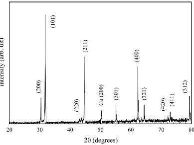
Figure 2 shows typical XRD patterns of Sn thin films electrodeposited at (a) 2.36 mA cm−2 and (b) 32.9 mA cm−2. Ten diffraction peaks indexed in Fig. 2 are consistent with those of polycrystalline -Sn [13]. According to the Sn phase diagram [11–12], the -Sn solid phase is stable at 0 C. However, there are no diffraction peaks of polycrystalline -Sn. For example, the diffraction peak from the (111) plane of polycrystalline-Sn appears at 23.75 degrees.
The phase transition between the -Sn and -Sn solid phases occurs at a critical temperature of 13.2 C [12]. In thermal equilibrium, the critical temperature is defined where the free energy of the -Sn solid phase is equal to that of the --Sn solid phase. In this study, a -Sn2+
ion in the solution becomes a Sn atom after it receives two electrons from the copper plate. As the -Sn solid phase does not emerge at 0 C, as shown in Fig. 2, the free energy of the Sn atom crystallized from the Sn2+
ion state may be different from that of a Sn atom in the solid phase represented by the Sn phase diagram [11– 12]. Hence, the critical temperature of a Sn atom during electrodeposition is different from 13.2 C.
Figure 2 also indicates that the ten crystallographic planes exist parallel to the copper plate. The (001) plane has the lowest surface energy among the (001), (110), and (100) planes [14]. When the current density is low, the crystallographic plane formed in a deposited film satisfies the surface energy minimum. However, the diffraction peak of the (001) plane, which has the lowest surface energy, is not observed as shown in Fig. 2. However, the diffraction peaks from the (110) and (100) planes do appear.
As a high-index plane generally has a large exchange current density, the high-index plane becomes dominant in the deposited film at a large the rectangular pulse current amplitude [15]. For example, the diffraction peak from the (321) plane in Fig. 2 (b) becomes stronger than that in Fig. 2 (a) in comparison to the diffraction peak from the (101) plane.
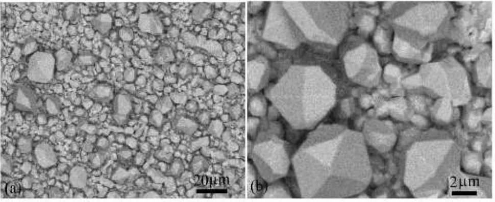
Figure 3. SEM images of Sn thin films electrodeposited at (a) 2.36 mA cm−2, (b) 11.8 mA cm−2, and (c) 32.9 mA cm−2.
[image:4.596.72.524.470.595.2]
width of approximately 8 and 5 m, respectively. As the Sn film thickness in Fig. 3 (a) is approximately 6 m, the dimensions of the Sn whisker are anomalous. In a further study, we will report the Sn whisker growth at 0 C in detail.
Three whisker growth mechanisms, i.e., the dislocation theory mechanism, recrystallization mechanism, and compressive stress related mechanism were proposed to explain anomalous whisker growth [9]. However, these mechanisms cannot explain the Sn whisker growth observed in Fig. 3 owing to the low deposition temperature of 0 C.
As shown in Fig. 3, the Sn whisker grew from the smooth Sn surface. Hence, the growth mode of the Sn thin film is the Stranski–Krastanov mode [15].
3.2. Sn thin films electrodeposited on copper plates at 9 C
Figure 4. XRD pattern of a Sn thin film electrodeposited at 23.2 mA cm−2. The Sn film thickness is 6.6 m.
[image:5.596.104.493.289.581.2]
Figure 5. SEM images of Sn thin films electrodeposited at 23.2 mA cm−2. (b) SEM image of large Sn whiskers.
Figure 5 shows SEM images of a -Sn thin film electrodeposited at 23.2 mA cm−2
. The surface of the Sn thin film looks like an aggregation of pebbles laid all over the surface. As shown in Fig. 5 (b), the Sn whisker shape is a polygonal prism surrounded by several crystallographic planes. Large Sn whiskers more than 14 m in size were grown on the Sn thin film. As the Sn film in Fig. 5 is approximately 6.6 m thick, the growth rate of the pebble seems to be anomalous.
3.3 Sn thin films electrodeposited on copper plates at 40 C
Figure 6 shows XRD patterns of Sn thin films electrodeposited at (a) 11.8 mA cm−2 and (b) 23.2 mA cm−2. Eleven diffraction peaks indexed in Fig. 6 are consistent with those of polycrystalline -Sn [13]. The diffraction peak from the (400) plane that does not appear in Figs. 2 and 4 is observed. As the -Sn solid phase is stable above 40 C, according the Sn phase diagram [11–12], only the diffraction peaks from crystallographic planes of -Sn appear.
SEM images of -Sn thin films electrodeposited at (a) 11.8 mA cm−2
[image:6.596.58.543.75.273.2][image:7.596.116.478.83.446.2]
Figure 6. XRD patterns of Sn thin films electrodeposited at (a) 11.8 mA cm−2 and (b) 23.2 mA cm−2. The Sn thin films are (a) 5 m and (b) 4.9 m thick.
[image:7.596.76.521.522.706.2]
Figure 8. Sn phase diagram for a deposition temperature and an amplitude of the rectangular pulse current. The dotted line shows the critical temperature of 13.2 C.
The XRD patterns of the electrodeposited Sn films are summarized in Fig. 8 as a phase diagram that represents the effect of changes in the deposition temperature and rectangular pulse current amplitude on the crystal structure of Sn. Figure 8 indicates that there is no -Sn solid phase (diamond structure) over the entire temperature range. The dotted line indicates the critical temperature of 13.2 C from in the previous Sn phase diagram. However, the Sn thin film electrodeposited at a temperature below 13.2 C has a tetragonal crystallographic structure.
3.4 Sn thin film electrodeposited on an ITO glass at 0 ℃
[image:8.596.140.450.73.387.2]
Figure 9. XRD pattern of a Sn thin film electrodeposited on an ITO glass at 23.2 mA cm−2 and 0 C. The Sn thin film is 5 m thick.
4. CONCLUSIONS
The phase diagram of Sn thin film generated by rectangular pulse current was obtained using XRD. The XRD analysis showed that the -Sn phase was stable, regardless of the deposition temperature and rectangular pulse current amplitude. SEM observations of the -Sn thin film indicated that the Sn whisker surrounded by crystallographic planes was grown at an anomalous growth rate. The growth mode of the Sn thin film was Stranski–Krastanov.
References
1. F. C. Walsh and C. T. J. Low, Surf. Coat. Technol., 288 (2016) 79. 2. S. Bakkali, A. Benabida, and M. Cherkaoui, Med. J. Chem., 6 (2017) 15.
3. Y. Wang, J. Zhou, W. Lvb, H. Fang, and W. Wang, Appl. Surf. Sci., 362 (2016) 394.
4. W. Lv, J. Zhou, J. Bei, R. Zhang, F. Kong, and W. Wang, Int. J. Electrochem. Sci., 11 (2016) 6183. 5. S. Balaji, M. A. Kumar, T. Manichandran, and D. Mutharasu, Russ. J. Electrochem., 52 (2016) 264. 6. V. Borra, D. G. Georgiev, and C. R. Grice, Thin Solid Films, 616 (2016) 311.
7. J. Cheng, P. T. Vianco, B. Zhang, and J. C. M. Li, Appl. Phys. Lett., 98 (2011) 241910. 8. K. N. Tu and J. C. M. Li, Mater. Sci. Eng.: A 409 (2005) 131.
9. P. Zhang, Y. Zhang, and Z. Sun, J. Mater. Sci. Technol., 31 (2015) 675.
Microelectron. Reliab., 55 (2015) 180.
11.G. Zeng, S. D. McDonald, Q. Gu, S. Matsumura, and K. Nogita, Cryst. Growth Des., 15 (2015) 5767.
12.A. Skwarek, P. Zachariasz, J. Zukrowski, B. Synkiewicz, and K. Witek, Mater. Chem. Phys., 182 (2016) 10.
13.H. E. Swanson and E. Tatge, Standard X-ray Diffraction Powder Patterns, NBS Circular 539, Vol. 1 (1953).
14.L. Vitos, A.V. Ruban, H. L. Skriver, and J. Kollár, Surf. Sci., 411 (1998) 186. 15.M. Saitou, Int. J. Electrochem. Sci., 12 (2017) 2719.
16.G. T. Galyon, IEEE Trans. Electron. Packag. Manuf., 28 (2005) 94. 17.K. -S. Kim, C. -H. Yu, and J. -M. Yang, Thin Solid Films, 504 (2006) 350.
18.H. Teller, S. Ohanona, D. Kashyap, and A. Schechter, J. Mater. Sci., 51 (2016) 8471.
19.D. Bunyan, M. A. Ashworth, G. D. Wilcox, R. L. Higginson, R. J. Heath, and C. Liu, Trans. Inst. Met. Finish, 91 (2013) 249.