Full length article
Cross-correlation based high resolution electron backscatter
diffraction and electron channelling contrast imaging for strain
mapping and dislocation distributions in InAlN thin
fi
lms
A. Vilalta-Clemente
a,*, G. Naresh-Kumar
b, M. Nouf-Allehiani
b, P. Gamarra
c,
M.A. di Forte-Poisson
c, C. Trager-Cowan
b, A.J. Wilkinson
aaDepartment of Materials, University of Oxford, Oxford OX1 3PH, United Kingdom bDepartment of Physics, SUPA, University of Strathclyde, Glasgow G4 0NG, United Kingdom cIII-V Lab, Thales Research and Technology, 1 Av. Augustin Fresnel 91767, Palaiseau, France
a r t i c l e i n f o
Article history:
Received 18 July 2016 Received in revised form 11 November 2016 Accepted 15 November 2016
Keywords:
EBSD ECCI Dislocations InAlN HEMTs
a b s t r a c t
We describe the development of cross-correlation based high resolution electron backscatter diffraction (HR-EBSD) and electron channelling contrast imaging (ECCI), in the scanning electron microscope (SEM), to quantitatively map the strain variation and lattice rotation and determine the density and identify dislocations in nitride semiconductor thinfilms. These techniques can provide quantitative, rapid, non-destructive analysis of the structural properties of materials with a spatial resolution of order of tens of nanometers. HR-EBSD has a sensitivity to changes of strain and rotation of the order of 104and 0.01 respectively, while ECCI can be used to image single dislocations up to a dislocation density of order 1010 cm2. In the present work, we report the application of the cross-correlation based HR-EBSD approach to determine the tilt, twist, elastic strain and the distribution and type of threading disloca-tions in InAlN/AlN/GaN high electron mobility transistor (HEMT) structures grown on two different substrates, namely SiC and sapphire. We describe our procedure to estimate the distribution of geometrically necessary dislocations (GND) based on Nye-Kroner analysis and compare them with the direct imaging of threading dislocations (TDs) by ECCI. Combining data from HR-EBSD and ECCI obser-vations allowed the densities of pure edge, mixed and pure screw threading dislocations to be fully separated.
Crown Copyright©2016 Published by Elsevier Ltd on behalf of Acta Materialia Inc. This is an open access article under the CC BY-NC-ND license (http://creativecommons.org/licenses/by-nc-nd/4.0/).
1. Introduction
Alloys of indium and aluminium containing nitrides (InAlN) are of great interest for the GaN based opto-electronics and micro-electronics industries. When the InN composition is between 16 and 18%, InAlN can be lattice matched with GaN and has a band gap ofz4.2 eV[1]. Their applications span from distributed Bragg re-flectors (DBRs) to high electron mobility transistors (HEMTs) where they improve performance by avoiding the strain due to the lattice mismatch which is inherent to AlGaN[1,2]. For DBRs, the use of InAlN achieves a high refractive index and within a lattice mismatch of±0.5%, it has been shown that no strain relaxations
takes place in the 16e20% InN composition range[1]. In the case of HEMTs, the situation may be more complex, as was shown by Kuzmík[2], not only is it of importance to minimize the strain by replacing AlGaN with InAlN, but one can also improve considerably the two dimensional electron gas (2DEG) by introducing an ultra-thin AlN interlayer between GaN and InAlN[2,3].
In recent years great progress has been made in producing good quality InAlN/GaN HEMTs and DBRs[4e6]. In the horizontal and close coupled showerhead reactors, growth conditions and composition can be modified to intentionally dope gallium (Ga) into nominal InAlNfilms up to several percent, as already reported [7,8], forming InAlGaN quaternary layers. Most of the hetero-structure materials are still epitaxially grown on foreign substrates such as sapphire, SiC and Si due to the lack of low cost and large size commercial GaN substrates. A high density of threading disloca-tions (TDs) is therefore generated in the material as a result of large lattice and thermal expansion coefficient mismatches between the
*Corresponding author.
E-mail address: [email protected] (A. Vilalta-Clemente).
Contents lists available atScienceDirect
Acta Materialia
j o u rn a l h o m e p a g e : w w w . e l s e v i e r . c o m / l o c a t e / a c t a m a t
http://dx.doi.org/10.1016/j.actamat.2016.11.039
1359-6454/Crown Copyright©2016 Published by Elsevier Ltd on behalf of Acta Materialia Inc. This is an open access article under the CC BY-NC-ND license (http://
GaN film and the foreign substrates. Considering the lattice distortion that surrounds dislocations and the potential for Coulombic interaction between electrons and charged dislocation lines, TDs could have a significant effect on 2DEG density. Such dislocations act as scattering centres and reduce the electron mobility in these heterostructures, especially when the sheet concentration is low or when an AlN interlayer is present [9]. Quantification of the TDs density and their types (screw, edge or mixed) is needed to diagnose their influence on optical and elec-trical properties, since not all dislocation types may be detrimental to device performance[10].
In addition to TDs, strain also has a profound effect on material properties, e.g. it can change the electronic band structure [11] which it is necessary to understand to optimise/engineer any electronic devices. The capability to evaluate the strain variation, lattice rotation and the distribution of TDs and resolve their types rapidly with negligible sample preparation would represent a real step forward in the development of more efficient nitride semi-conductor devices. This is the main focus of our present work.
The analysis of defects and deformation is commonly performed by transmission electron microscopy (TEM). However, such ana-lyses require a sample thinning process to obtain an electron transparent specimen, which is highly intrusive and involves an irreversible alteration of the internal strainfield. It is possible to differentiate between dislocations with a screw component (those which terminate a step) and pure edge dislocations (those that do not terminate a step) using atomic force microscopy (AFM). TDs form small pits when they terminate at the sample surface and this change in the topography can be detected by AFM. In addition to their location with respect to any observed atomic steps, the size of the pits has been found to be related to the dislocation type, with the pits due to pure edge dislocations being smaller than those containing a screw component[12]. Detection of the pits need a sharp AFM tip and clean surfaces and the detection of the pits can be facilitated by surface treatment[13]. In the case of III-nitrides, the surface may be subjected to an in situ treatment using SiH4 and NH3immediately after growth, which enlarges the size of the pits and making it easier to detect the dislocations using AFM[14]. X-ray diffraction (XRD) methods have also been used[15]however their application becomes more difficult as layer thickness is reduced and layer quality is improved. The crystal mosaicity model has been adapted for analysis of nitrides[15]in which the tilt of the (0001) oriented layer can be correlated to the density of screw threading dislocations and the lattice twist can be correlated to the density of edge dislocations. Metzger et al.[16]demonstrated for GaN layers the connection of threading edge dislocations to in-plane mosaic and threading screw dislocations to out-of-in-plane mosaic. They noted from TEM that almost all TDs ran parallel to the surface normal direction [16,17]. Thus the twists within the layer are due to the edge components of TDs, while tilts result from screw components. Quantification of diffraction peak broadening for reflectors at different inclination from the surface normal allows the density of screw and edge dislocations to be determined separately[16].
Scanning electron microscope (SEM) based electron diffraction techniques such as electron backscattered diffraction (EBSD) and electron channelling contrast imaging (ECCI) offer both high reso-lution and non-destructive analysis of defects and deformation. The introduction of cross-correlation based analysis of EBSD patterns has seen a step change in the angular resolution toz104rad[18] which is sufficient to enable analysis of the misorientations and local elastic strainfields that are typical in nitride semiconductor materials. The relatively new cross-correlation based analysis of EBSD patterns offers considerably higher precision than the con-ventional Hough based analysis to study the strain and rotation
gradients[19]. Thus with the help of the HR-EBSD, it is possible to measure very small relative disorientation and strain in nitride semiconductor materials[20]with a very high precision of better than 0.01and about 104, respectively. HR-EBSD is based on the precise measurement of the small shifts of image features on an EBSD pattern (EBSP) by applying the cross-correlation analysis[18]. Using data from this analysis within the Nye-Kroner framework, it is also possible to estimate the density of geometrically necessary dislocations (GNDs) within the material measured from the lattice curvatures on the sample surface[21]. Recent advancement in ECCI for revealing and identifying threading dislocations (TDs)[22]and imaging stacking faults[23] makes ECCI ideal for characterising extended defects in nitride semiconductors. Combining HR-EBSD and ECCI will provide an efficient and fast approach to investigate the structural properties of nitride thin films, enabling crystal growers and device manufactures to produce ultra-fast and energy efficient electronic devices for example. These techniques will be invaluable analysis tools to the wider materials community requiring quantitative structural analysis of their materials. For example they may be applied for the strain and defect analysis of phosphide and telluride semiconductor thinfilms, SiGe, SiC and diamond thinfilms.
2. Experimental
2.1. Sample details
The HEMTs samples studied consist of two InAlN/AlN/GaN heterostructures grown by metalorganic vapour phase epitaxy (MOVPE) in an Aixtron AIX200RF horizontal reactor. The samples were grown on two different substrates, namely sapphire (Al2O3) and 4H-SiC. On both samples, the InAlN layer wasz15 nm. The thickness of the non-intentionally doped GaN buffer layer was 1.6
m
m for the sample grown on the AlGaN(nucleation layer)/SiC and 3m
m for the sample grown on the GaN(nucleation layer)/Al2O3. On top of the GaN buffer layer, a thin AlN interlayer ofz1 nm was grown at 1200C using H2as carrier gas. The temperature was then reduced to 865C for the growth of InAlN layer under nitrogen atmosphere. The InN content was slightly different for the two samples; 17.6±1% for the InAlN on Al2O3and 21.4±1% for the InAlN on SiC. The In composition was determined from XRD mea-surements [24]. For convenience hereafter we shall refer to the HEMT samples in accordance to the substrates they were grown on: InAlN on SiC and InAlN on sapphire. Prior to EBSD measurements, the samples were cleaned in an organic solvent followed by plasma cleaning forz3 min (Fishione 1020 plasma cleaner) after mounting on to an aluminium stub.2.2. Electron backscattered diffraction (EBSD)
2.2.1. Cross-correlation analysis
EBSD measurements were carried out using a Zeiss Merlin Field Emission Gun (FEG) SEM equipped with a Bruker eFlashHREBSD detector run with Esprit 1.9 software. In our present work, all the EBSPs were acquired using an electron beam energy of 20 keV and a probe current of 5 nA with a detector to screen distance of 18 mm. The EBSPs were acquired on a rectangular grid spanning 22.616.9
m
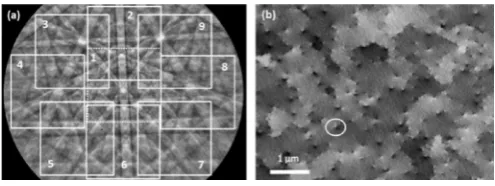
m2with a 200 nm step size. For each map a total of 9492 patterns were captured and recorded at the full resolution (16001200 pixels) of the EBSD camera. The samples were ori-ented such that the [0001] direction pointed out of the sample surface plane and the two perpendiculars [-1100] and [11-20] crystallographic directions pointed along the x1and x2specimen axes, where the x1axis aligns with the sample tilt axis.In cross-correlation based EBSD all the test patterns within a map are compared to a selected reference pattern using cross-correlation of pattern intensities within a number of regions of interest (ROIs). An example EBSP obtained from the InAlN on SiC is given in Fig. 1(a), and the white squares represent ROIs (nine selected in this instance). Cross-correlation algorithms find the translation between two matched regions within the patterns be-ing compared and extract a translation (shift) along both x1and x2 directions (from the cross-correlation peak position), in addition to a measure of how good the best pattern matching is (from the normalised cross-correlation peak height).
Cross-correlation analysis of the patterns was conducted off-line using the method described in Ref.[18]. Pattern shifts were deter-mined from 35 ROIs of each pattern with a band passfilter applied in the Fourier domain to remove high frequency noise and low frequency background intensity variations. One pattern was selected as the reference and all the measurements are made relative to this. The shape change and rotation of the crystal lattice can be linked to the measured pattern shifts and can be used with knowledge of position vectors describing the dispersion of ROIs across the EBSD detector relative to the diffracting volume on the sample using a set of simultaneous linear equations described in Ref.[18]. To separate the normal strains a boundary condition is employed which forces the stress
s
33normal to the sample surface to zero in the near surface region from which EBSD originates[19]. This allows the normal strains to be related via:s
33¼0¼C33 333þC32 322þC32 311 (1)The elastic constants used in this study are C13¼99 GPa and C33¼389 GPa for AlN[28], and C13¼92 GPa and C33¼224 GPa, for InN[29]. For the InxAl1-xN ternary alloy, stiffness coefficients were obtained by the corrected Vegard's law given by Darakchieva et al. [30].
This generates maps of the variation of elastic strain (3 ij) and
lattice rotation (
u
ij) relative to that at the reference point. Note the strain state is unknown at the reference point (the so-called‘reference pattern problem’) [19]. The elastic strains and lattice rotations are defined as the symmetric components and anti-symmetric components of the displacement gradient tensor respectively as shown in the following three equations:
Elastic normal strain
3ii¼ vui=vxi (2)
Elastic shears strains
3ij¼ 1=2*vuivxjþvujvxi (3)
Lattice rotations
u
ij¼ 1=2*vui
vxjvuj
vxi
(4)
wherexiis a direction in the crystal anduiis a displacement in the
ith direction. Normal strain with positive values corresponds to tensile strain and negatives values correspond to compressive strain. Further details of the strain analysis and the displacement gradient can be found in Refs.[18,19,31]. For the rotation term,
u
12 is the in plane rotation or twist about the surface normal x3andu
13 andu
23are the two out of plane rotations or tilts about x2and x1 respectively.2.2.2. Geometrically necessary dislocation (GND) density analysis Geometrically necessary dislocation (GND) density corresponds to the density needed to accommodate the lattice distortion measured for a given area; that is they are required to account for a closure failure of the Burgers circuit around the measurement area [32e34]. Thus a Burgers circuit construction around an arbitrary group of dislocations reveals that only a fraction of them contribute to the net Burgers vector and thus correspond to the GND density. While, in contrast, other dislocation structures such as dipoles, multipoles and loops wholly contained with the Burgers circuit contribute a null net Burgers vector, and result in no lattice cur-vature at the length scales of the Burgers circuit under consider-ation. This latter contribution to the dislocation density is classified as the statistically stored dislocation (SSDs) density[32e36].
Dislocation densities estimates using EBSD are generally per-formed according to Nye's theory[32], where rotation gradients within a Burgers' circuit are linked to the stored GND. Kroner[33] extended this analysis to include the elastic strain gradients that Nye had assumed to be small. Nye's assumption has been found to be reasonable in deformed metals but in semiconductors the elastic strain gradients could make significant contributions and should not be neglected. When elastic strain gradients are included in the analysis only three of the nine terms in the Nye-Kroner dislocation tensor can be found and these relate to dislocation types with lines that propagate to the sample surface along x3 [37] Equations (5)e(7)relate terms in the Nye-Kroner dislocation tensor
a
ijwith the lattice curvature. Thefirst two equations concern the twist (u
12) and the third concerns the tilt (u
13andu
23). In the InAlN thinfilms, we assume that the three measured lattice curvatures (rotation and elastic strain gradients) are accommodated by combinations of screw dislocations along [0001], and three possible edge disloca-tion types with [0001] line direcdisloca-tion and 1/3<1120>Burgers vector(ie 1/3ai, i¼1,2,3).
a
13¼ 1 3X3
i¼1
ai$½100
r
i¼ vuvx121 þ
v311
vx2 v312
[image:3.595.44.292.611.704.2]vx1 (5)
a
23¼ 1 3X3
i¼1
ai$½010
r
i¼v
u
12 vx2 þv312
vx2 v322
vx1
(6)
a
33¼ jcjr
<c>¼ vuvx132
vu23 vx1 þ
v 313
vx2 v 323
vx1
(7)
At each point in the map, a set of possible GND densities (
r
<c>,r
i,i¼1,2,3) that satisfies the three lattice curvature are found. The two twist equations(5)and(6)contain three unknowns (
r
i,i¼1,2,3) and so there can be many possible combinations that are valid solutions and we choose the one which gives the minimum total line energy (L1 optimisation)[21]. Equation(7)describing the lat-tice tilt provides an unambiguous estimation of the screw dislo-cation density (r
<c>).2.3. Electron channelling contrast imaging (ECCI)
Electron channelling contrast imaging (ECCI) can be used in a near normal incidence geometry[38,39]or in a forescattered ge-ometry where the sample is tilted from 30 to 70 toward the electron sensitive detector positioned to collect electrons scattered to low take-off angles. Electron channelling contrast images are produced when a sample is positioned so that a plane or planes may diffract the electrons incident on the sample. Changes in crystallographic orientation or changes in lattice constant due to local strain are revealed by changes in contrast in the channelling image constructed by monitoring the intensity of backscattered electrons as the focused electron beam is scanned over the sample. Extremely small changes in orientation and strain are detectable, revealing, for example, low angle tilt and rotation boundaries and atomic steps and enabling extended defects such as dislocations and stacking faults to be imaged.Fig. 1(b) shows one such image where TDs are revealed as spots with black-white contrast for the InAlN thinfilm grown on SiC. ECC images were acquired using an FEI Sirion 200 Schotty FEG-SEM with a beam current ofz2.5 nA, a beam divergence of z4 mrad, and an electron beam energy of 30 keV. In our present work, we use a forescatter geometry where the sample is tiltedz54to the impinging electron beam and the backscattered electrons are detected by an electron-sensitive diode from KE developments Ltd.
For materials with a wurtzite crystal structure such as GaN, we have previously developed a simple geometric procedure to iden-tify a given TD as edge (E), screw (S), or mixed (M) by exploiting differences in the direction of the blackewhite (B-W) contrast be-tween two ECC images acquired with symmetric diffraction con-ditions[22]. Knowledge of the diffraction conditions requires the acquisition of electron channelling patterns (ECPs) without which differentiating between different dislocation types is not possible, especially between pure screw and mixed dislocations in nitride semiconductors. However by comparing the B-W contrast di-rections of TDs between two ECCI micrographs obtained from the same region of the sample at different (though unidentified) diffraction conditions, it is possible to differentiate between pure edge type dislocations and dislocations with screw component (pure screw and mixed dislocations) [40]. In the present work, acquisition of good quality ECPs was not possible due to the sam-ples' surface topography.
3. Results
3.1. Cross-correlation EBSD
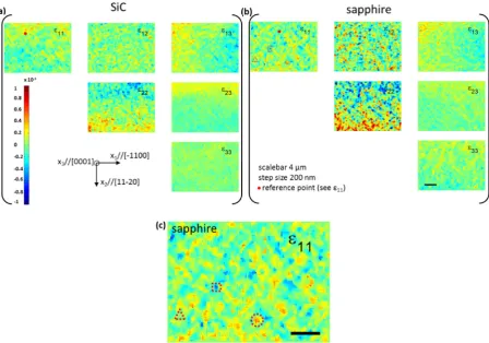
The residual strain maps obtained using the cross-correlation
analysis for the two InAlN samples grown on the SiC and sap-phire substrates respectively are shown inFig. 2(a)e(b). Please note the resulting frame used to describe the strain state from the EBSPs has the x1direction which corresponds to the InAlN crystal direc-tion of [-1100], the x2direction corresponds to the [11-20] and the x3direction corresponds to the [0001] surface normal as is illus-trated inFig. 2(a). The reference point is a user selected option, in our measurements we have selected an area toward the top left corner of the map as indicated for each sample on the 3 11strain map
by a red circle (seeFig. 2). The maps produced represent the vari-ation in elastic strain with respect to the marked reference point. The same colour scale (blue to red) is used for each strain map on both samples. Ultimately, regions with high tensile strain are indicated in red (dotted circle on 3 11 in Fig. 2(b)), regions with
compressive strain are indicated in blue (dotted rectangle) and regions with lower strain or no strain are indicated in green (dotted triangle). This can be clearly seen in the enlarged section of the 3 11
map shown inFig. 2(c). Comparing the six strain component maps it may be discerned that the higher strain variations are for the in-plane shear strain, 3 12and the two in-plane normal strains, 3 11and 3 22for each sample. This behaviour is consistently observed for both
samples. This may be due to the difference in thermal expansion coefficient between GaN, InAlN and the lattice mismatch along the two in-plane directions driving the formation and arrangement of dislocations. In addition the lattice constants and in-plane thermal expansion coefficient of the GaN differ from those of both sapphire and SiC, and this results in-plane strain of InAlN on both different substrates[29]which will also lead the formation of dislocation. The lattice constants and in-thermal expansion coefficients[29]of SiC are closer to those of GaN compared to sapphire, therefore the GaN layers grown on SiC have better crystalline quality.
The variation in the two out of plane shear strains (3 13and 3 23)
and the out of plane normal strain (3 33) remains close to zero in
accordance with the expectation that the corresponding out of plane stresses should be zero to comply with the biaxial strain in the epitaxially grown InAlN layer.
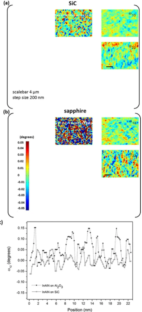
The out of plane lattice rotation
u
23, is defined as the rotation about the x1axis i.e. [-1100] of the specimen, andu
13is the rotation about x2 i.e. [11-20], whileu
12 is the in-plane rotation corre-sponding to a twist about the surface normal x3i.e. [0001]. Maps of these lattice rotationfields are shown inFig. 3for both samples. It can be seen that the magnitude of the in-plane rotation is signifi -cantly greater than those out of plane. This behaviour is seen for both samples. When comparing the rotation maps, the lattice rotation on sapphire is much greater than on SiC in accord with the larger lattice mismatch between GaN and the sapphire substrate. The scale inFig. 3(b) shows both positive and negative values to represent the in-plane rotation directions with respect to the reference point. As InAlN has a lattice mismatch with respect to the GaN layer and substrate underneath, mosaic structures of misor-iented sub-grains can be formed. The coalescence of islands during the growth can form the misoriented sub-grains. Due to the epitaxial growth processes, these misorientations are extremely small when compared to polycrystalline samples. The white dotted lines (see Fig. 3(a)e(b)) marks the trace of line scans of twist rotation (u
12) with respect to the reference point for both the samples.Fig. 3(c) shows the lattice rotation profile for the line scans along the marked dotted white lines. The maximum in-plane rotation for the InAlN on sapphire is just above 0.15, whereas the maximum for the InAlN on SiC is lower than 0.05. Therefore, in-plane rotation is lower for the sample with smaller lattice mismatch between the GaN layer and substrate.components about the mean value for both the samples. It can be seen fromFig. 4(a) that the normal in plane strains (3 11, 3 22) have a
wider range of strain distribution than the normal out of plane strain (3 33) for both the samples. The in-plane shear strain (3 12)
distribution measured for the sapphire substrate sample is mark-edly wider compared with the out shear strains (3 23, 3 13). On the
rotation histograms, the distributions show a larger spread in the twist mosaic (Fig. 4(c)) compared to the tilt mosaic and the spread is largest for the twist mosaic in the sample grown on the sapphire substrate. This is visually evident from the maps shown in Fig. 3(a)e(b). A larger spread for the twist mosaic when compared to that of tilt was also observed in the Hough transformed based EBSD measurement by Rao et al.[41]and cross-correlation method by Wilkinson [37] on GaN thin films. This is comparable with previous measurements of the in-plane twist and out-plane tilt in GaN using TEM[42,43]and XRD[16,44].
3.2. GND density analysis
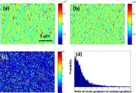
Although the elastic strain variations shown inFig. 2are smaller than the lattice rotations shown inFig. 3, the difference does not appear so large that neglect of the elastic strain gradient seems obviously justified in analysing the GND density content. A more direct comparison is made inFig. 5which compares two terms in equation (5) for the GND density: one lattice rotation gradient
vu12
vx1
inFig. 5(a) and one elastic strain gradient term
v312 vx1
in
Fig. 5(b), whileFig. 5(c) shows the ratio
v312 vx1=
vu12 vx1
between the two
terms. The strain gradient is often close to or sometimes signifi -cantly in excess of the rotation gradient in this sample, indeed z50% of the points have a ratio of unity or above (Fig. 5(d)). This provides ample demonstration of the need to include elastic strain gradient terms when evaluating the GND density.
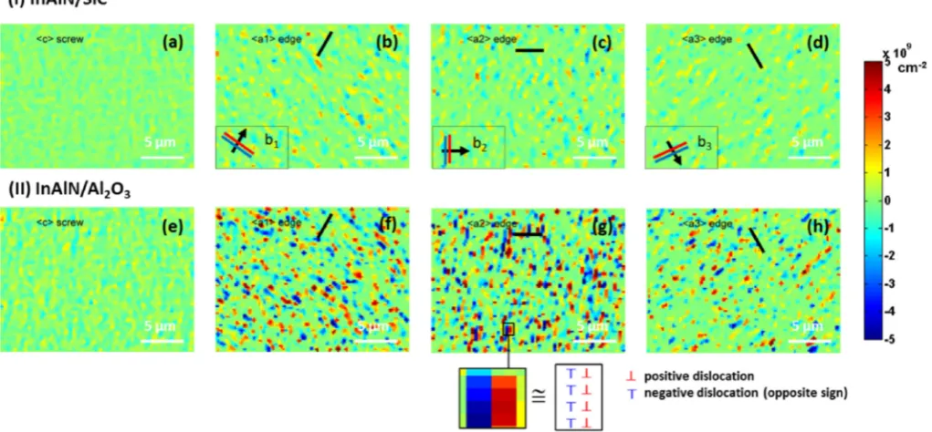
Solving equations(5)e(7) from the Nye-Kroner theory allows the TD density to be estimated. The screw GND density is found directly from equation(7), while the two equations(5)and(6)are used in combination with the constraint that the energy be mini-mised to establish the densities of the three edge GND types. Fig. 6(a)e6(d) andFig. 6(e)e6(h) show the distribution of four types (1 screw and 3 edge) of TDs in (I) InAlN/SiC and (II) InAlN/Al2O3 respectively. For the<c>screw GNDs (Fig. 6(a)e(e)), the positiveb is parallel to the line direction of the dislocation along the outward surface normal. The Burgers vectors of the edge dislocations<ai> are marked by black lines toward the top of the GND density maps inFig. 6(b)e6(d) andFig. 6(f)e6(h). The sense of the Burgers vector for positive dislocations (with line direction along the outward surface normal) are indicated by black arrows shown inFig. 6(b)e
[image:5.595.80.529.65.379.2]6(d). The meaning of positive/negative GND density in these maps (Fig. 6) is that GNDs are present at the absolute density shown but with a positive or negative Burgers vector given by the sign of the colourscale (red/positive, blue/negative). It is noticeable that there tends to be an alignment of the edge GND densities into short bands of raised GND density (of a particular sign) running perpendicular to the Burgers vector for each of the edge GND density maps. This corresponds to an equilibrium configuration of the dislocation types in an array of edge dislocations one above the
Fig. 2.Residual strain mapped by EBSD for InAlN thinfilm samples grown on two different substrates (a) SiC and (b) sapphire. The red dot on 3 11is the EBSP reference point. The
dotted circle, triangle and rectangle on 3 11map highlight areas with tensile, no strain and compressive strain along the [-1100] direction on InAlN/Al2O3. (c) Enlargement of 3 11map
on InAlN/Al2O3. The same colour scale is used for each strain map. The reference axis and crystallographic system is also shown in thefigure. (For interpretation of the references to
other in a (very) low angle tilt boundary[45]. This often seems to happen with a band of positive GNDs running next to one with negative GNDs e.g. black rectangle inFig. 6(g). Note the width of the bands (red or blue colour) correspond toz2 pixels which arises as a results of the 3 by 3 pixel wide patch used for numerical evalu-ation of the rotevalu-ation and strain gradients, which in convolution
with an abrupt change in rotation or strain, generates a 2 pixels wide region of high strain gradient. This ‘blurs’ the individual dislocation images that can be identified in ECCI images (seeFig. 7) into a distribution of dislocation density.Fig. 6indicates a signifi -cant difference in the dislocation density of edge type dislocations when compared to screw for both the samples. Also it can be seen that the total threading dislocation density is higher in InAlN/Al2O3 when compared to InAlN/SiC. The average densities of screw and edge GNDs are given inTable 1for the two samples. The step size clearly has implications for the measured GND density[21]since if the step size is too large then multiple dislocations will thread the patch and only their combined excess Burger vector contributes to the curvature measured across the patch while components that cancel in the vector summation are not measured. The step size was thus kept relatively small (200 nm) to avoid excessive underesti-mation of the density and seven different regions in each sample, covering a total area of 2680
m
m2, were analysed and the results averaged to ensure a good representative sampling of the distri-bution. The error reported inTable 1is the standard deviation be-tween the average density values obtained for each of the seven randomly scanned areas.It is also possible to estimate the TD density from the tails of residual stress probability distributions P(
s
12) [46]. The high stresses near a dislocation core are such that random sampling leads to a probability distribution that follows a high stress asymptote withP(s
)f1/s
123, as shown by Groma et al.[47]and Kaganer et al.[48]Kaganer et al.[49]have used such analysis and X-ray diffraction peak tails to determine TD densities in GaN epitaxial films. We recently analysed HR-EBSD generated stress probability distributions from these two InAlN samples and ob-tained the combined density of edge and mixed dislocations from the in-plane shear stress results as is shown inTable 1 [46].3.3. ECCI
In order to image sub-grains and resolve individual TDs, deter-mine their types and estimate their densities, we have performed ECCI.Fig. 7(a)e7(b) and 7(c)e7(d) show the ECCI of InAlN/SiC and InAlN/Al2O3respectively. As mentioned previously, it is possible to distinguish between dislocations with a screw component (i.e. pure screw or mixed) and pure edge dislocations by monitoring the B-W contrast direction associated with TDs taken from two ECC images acquired from the same part of the sample with different diffraction conditions. This is illustrated inFig. 7where the white rectangles show pure edge dislocations for which the sense of the B-W contrast seen in Fig. 7(a) (and 7(c)) is reversed in direction in Fig. 7(b) (and 7(d)), this is not the case for dislocations with a screw component (see white circles inFig. 7). Change in contrast of the sub-grains is also observed on changing the diffraction conditions, this can be seen clearly in the InAlN/Al2O3(seeFig. 7(c)e(d)). The sub-grain contrast can be attributed to variation in the orientation of the sub-grains and the larger sub-grain contrast observed for the InAlN/Al2O3can be qualitatively attributed to a higher variation in rotations for this sample observed in the quantitative HR-EBSD results (Fig. 3(b)). Note that dislocations line up along the sub-grain boundarieseour analysis reveals theses dislocations to be edge dislocations. This is consistent with the alignment of the edge GND densities observed inFig. 6.
TD densities and types were estimated from ECCI by manually counting dislocations in the acquired images and identifying those which reverse their B-W contrast on changing the diffraction vec-tor. To determine total dislocations density, observations were made on three differentz18
m
m2regions of each sample. The error reported inTable 1is the standard deviation between the average density values obtained for each of the three areas. For each sample,Fig. 3.Variation in lattice rotations for the scanned region (a) InAlN/SiC and (b) InAlN/
Al2O3. All the variations are measured with respect to the reference point indicated by
the red dot inFig. 2(c)u12lattice rotation profile for the selected lines on the maps.
(For interpretation of the references to colour in thisfigure legend, the reader is
[image:6.595.40.284.66.603.2]z170 dislocations were analysed to estimate the TD types. The densities of pure edge TDs and those with some screw character (pure screw and mixed) are given inTable 1, the errors reported are the standard deviation derived from the count of each dislocation type. It should be noted that HR-EBSD and ECCI were not performed from the same area.
4. Discussion
EBSD is a surface sensitive technique and the Kikuchi band signal with EBSD patterns originates from the near surface region.
[image:7.595.54.558.65.229.2]The exact depth sensitivity of EBSD is in fact rather poorly known but often it is stated to be in the range between 10 and 40 nm at 20 kV, with the lower values reached for denser material[50]and with lower depth penetration expected for lower accelerating voltage and higher atomic number of the specimen[51]. Zaefferer [52]has made measurements from amorphous chromium layers on a Si single crystal and shown that at 15 keV only a 2 nm Cr layer reduced the contrast of the substrate pattern to half its value from the uncoated Si. The most comprehensive and recent analysis has been given by Winkelmann et al. who performed Monte Carlo simulations incorporating discrete inelastic scattering events. They
Fig. 4.Distribution of (a) normal strain, (b) shear strain and (c) twist (u12) and tilt (u13andu23) in InAlN on SiC (open circles) and InAlN on Al2O3(lines).
[image:7.595.77.527.269.576.2]associate the Kikuchi band contrast with electrons scattered through large angle in their last elastic interaction before leaving the sample and show the depth distribution of such electrons fol-lows and exponential decay with an attenuation length of 22 nm in Si for 20 keV and 10e12 nm for 10 keV incident electrons[53]. The average atomic number of the InAlN layer at ~20% In is very close to that of Si, however the significantly higher Z2value of In makes it a more effect large angle scatter centre. Taking the 22 nm attenuation length suggested for Si at 20 keV by Winkelmann we would expect ~50% of the EBSD signal to originate from within the 15 nm
thickness of the InAlN layer. Some HR-EBSD measurements were also made at other beam energies from 15 keV to 30 keV and a slight tendency for higher GND densities at lower beam energies was observed.
Generally in nitride thinfilms, the density of pure screw dislo-cations is between 1 and 10% of the total TDs[54,55]. However the ratio of mixed to pure edge dislocations is variable[56]. From our present EBSD analysis, we cannot differentiate between pure edge and mixed dislocations. Similarly, for the ECC images used here, without knowledge of the diffraction conditions, it is not possible to differentiate between pure screw and mixed dislocations. We have previously made TEM observations on cross-section samples of these materials in which weak beam imaging with (0002) and (11-20) reflections was used to distinguish pure screw, mixed and pure edge dislocations[24].
The GND density analysis of the nitride thinfilms as described here, is similar to XRD analysis and can be thought of in terms of the crystal mosaicity model [15]. Metzger et al. [16] separated the density of edge (z1010cm2) and screw (z2108cm2) TDs in GaN layers from measurement of peak widths for 5h0hl
[image:8.595.39.550.73.310.2]asym-metric reflections and for 3 ð000lÞ symmetric reflections,
Fig. 6.Maps showing a low energy solution for the<c>screw GNDs and the three<ai>edge dislocation density distributions in (I) InAlN/SiC and (II) InAlN/Al2O3. The black line
indicates the Burgers Vector direction. Colourscale gives the positive (┴, red colour) and negative (┬, blue colour) sense of the dislocation's bands. Note the right black rectangle
shows the sign of the distribution dislocations. As example, two opposite alignment of four dislocations are drawn. (For interpretation of the references to colour in thisfigure
legend, the reader is referred to the web version of this article.)
Fig. 7.ECCI micrographs exhibiting sub-grain contrast and showing threading dislo-cations. The circles highlight dislocations with a screw component and the rectangles
highlight pure edge type dislocations: (a)e(b) ECCI of InAlN/SiC, and (c)e(d) ECCI of
[image:8.595.36.281.380.573.2]InAlN on sapphire acquired under different diffraction conditions.
Table 1
Threading dislocation density measured by HR-EBSD and ECCI techniques. The
values are given in cm2.
Method TDs (x109cm2) Samples
InAlN/SiC InAlN/Al2O3
HR-EBSD Screw type (MþS) 0.20±0.09 0.40±0.06
Edge type (MþE) 1.50±0.29 3.50±0.42
Total 1.70±0.38 3.90±0.48 ECCI Screw type (MþS) 0.5±0.1 1.1±0.2
Pure edge (E) 1.0±0.1 2.3±0.2
Total 1.5±0.1 3.4±0.5
Wilkinson et al.a MþE 1.4 4.1
[image:8.595.304.553.642.733.2]respectively. In their case TEM showed somewhat higher densities for the edge dislocations atz1011cm2, and screw dislocations at 8108cm2and mixed dislocations were observed at a density of z108cm2. The presence of mixed dislocations was neglected in the analysis of X-ray data as an unambiguous separation is only possible for pure edge and pure screw dislocation types.
A similar issue is found in the analysis of GND density from HR-EBSD data. Adding mixed dislocations into the analysis generates a further 6 dislocation types (and their negative counterparts) so that the three equations(5)e(7)are fully coupled and need to be solved for the densities of 10 dislocation types. The problem is poorly constrained and many possible solutions exist. Recourse to energy minimisation is not helpful in removing the ambiguity as for isotropic elasticity, the mixed dislocation has the same energy as the pure screw and pure edge (as the Burgers vectors are orthog-onal) and generate the identical curvature. Anisotropic elastic strain energies from Foreman's analysis[57]suggest that a pair of pure screw and edge dislocations have lower energy than the equivalent mixed dislocation and so would be the energetically preferred solution (so the fields determined in Fig. 6 would be maintained). The presence of many mixed dislocations in these InAlN layers (from previous TEM analysis[24]) indicates that ki-nematics of the defect formation and/or core energies are also important. Core energies may be difficult to establish as In segre-gation to TDs has been seen experimentally using HAADF[58], linked to increased leakage currents[59]and in atomistic simula-tions has been seen to reduce core energies of screw TDs[60].
Neither HR-EBSD nor ECCI individually provide unambiguous separation of screw, edge and mixed TD densities, however, combining the information from the two techniques allows a simple set of four linear equations in the three unknown densities to be solved in a least squares sense, with the constraint that the densities are positive or zero. These fully separated dislocation densities are given inTable 2for the two samples.
Given the real region to region variations in dislocation densities and distribution across types, and the quite different measurement strategies, the quantitative comparison of dislocation densities summarised in Tables 1 and 2 is entirely reasonable. Certainly greater discrepancies have been reported between XRD and TEM methods on GaN[15]and here in the InAlN the densities are lower. The HR-EBSD based GND density measurements are generally considered to be lower bound estimates as only the excess Burgers vector within a grid square on the EBSD map contributes so if there are multiple dislocations within the grid square then some con-tributions may be lost due to cancelling in the vector sum of Bur-gers vectors.
The noisefloor for the HR-EBSD rotations isz104rad which at a step size of 200 nm gives an estimated minimum detectable GND density ofz5 108 cm2 for <a> type edge dislocations and z1108cm2for<c> type screw using the simple expression cited in Refs.[21,61]. These are below the average GND densities reported inTable 1, but only just so for the screw (plus mixed) type. The noise floor relates to the limited sensitivity of individual measurements within a map rather than uncertainty in the mean GND density values obtained. Measurement noise would be ex-pected to artificially increase the apparent GND density in regions of the sample where real dislocation content is below the noise floor. It is reassuring that the ECCI results in fact give slightly higher
densities for the screw and mixed TD types. In our analyses the step size was 200 nm, reducing the step size further in attempts to allow the resolving of the majority of GNDs would increase the noisefloor [61]and result in misinterpretation of the dislocation because the GND density will be close or below the noisefloor. For this instance of a sample with low density of dislocations it is suggested that is a good practice to obtain a few GND maps from different regions through the sample. It should also be borne in mind that the Nye-Kroner GND analysis was originally formulated on the basis of a relatively high density of dislocations (in deformed metals) that could be considered as a continuous distribution, while for these samples a single TD within a grid square corresponds to a density of 2.5109cm2. The average densities are close to or below this so the dislocations should really be analysed as discrete entities rather than a continuous dislocation densityfield.
5. Summary
The present work used HR-EBSD and the ECCI techniques to examine the lattice strain, lattice rotation and threading dislocation densities in InAlN thinfilms grown on SiC and sapphire. The key results of the investigation are summarised in the following:
1. HR-EBSD allows for the accurate determination of local strain gradients, combined with improved spatial and angular reso-lution and sheds new insight on dislocation distribution content in nitride thinfilms.
2. The substrates play a great role in affecting the in-plane strain (3 11, 3 22, 3 12) and the lattice rotations in the InAlN layers. The
variation in tilt and twist decreases with decreasing the mismatch between the GaN layer and the substrate. The significantly smaller rotations in the InAlN/SiC sample compared to the InAlN/Al2O3 sample indicate a lower defect density in the heterostructure grown on SiC.
3. The in-plane twist rotations were larger than the out-of-plane tilts for both samples indicating that the density of edge and mixed dislocations is greater than that for screw and mixed dislocations.
4. HR-EBSD measurements were analysed using Nye-Kroner the-ory to determine the density of edge and mixed GNDs, and screw and mixed dislocations. ECCI allowed pure edge disloca-tions to be distinguished from screw and mixed dislocadisloca-tions. Combining data from HR-EBSD and ECCI observations allowed the densities of pure edge, mixed and pure screw threading dislocations to be fully separated.
While we have demonstrated the application of the HR-EBSD and ECCI techniques to examine the lattice strain, lattice rotation and threading dislocation densities in InAlN thinfilms, the analysis as described in this paper is applicable to a wide range of materials including nitride, phosphide and telluride semiconductor thin films, SiGe, SiC and diamond thinfilms.
Acknowledgments
[image:9.595.39.569.85.120.2]We would like to acknowledge thefinancial support provided by the Engineering and Physical Sciences Research Council, UK via Grant Nos. EP/J015792/1 and EP/J016098/1 on “Nanoscale
Table 2
Dislocation densities estimated for different dislocation types from combined HR-EBSD and ECCI data.
Samples Method Screw (S) Mixed (M) Edge (E) Total TDs
InAlN/SiC HR-EBSD&ECCI Density109cm2 0.00 0.38 1.06 1.44
characterisation of nitride semiconductor thin films using EBSD, ECCI, CL and EBIC”and Grant No. EP/K032518/1 on“ Characterisa-tion of nanomaterials for energy”.
Data in support of this paper will be made openly accessible on the Oxford Research Archive (www.ora.ox.ac.uk).
References
[1] J.-F. Carlin, M. Ilegems, High-quality AlInN for index contrast Bragg mirrors lattice matched to GaN, Appl. Phys. Lett. 83 (2003) 668e670.
[2] J. Kuzmík, InAlN/(In)GaN high electron mobility transistors: some aspects of the quantum well hetersotructure proposal, Sci. Technol. 17 (2002) 540e544. [3] M. Gonschorek, J.-F. Carlin, E. Feltin, M.A. Phy, N. Grandjean, High electron mobility lattice-matched AlInN/GaNfield-effect transistor heterostructures, Appl. Phys. Lett. 89 (2006) 062106.
[4] F. Medjdoub, R. Kabouche, A. Linge, B. Grimbert, M. Zegaoui, P. Gamarra, C. Lacam, M. Tordjman, M.A. di Forte-Poisson, High electron mobility in high-polarization sub-10 nm barrier thickness InAlGaN/GaN heterostructure, Appl. Phys. Express 8 (2015) 101001.
[5] A. Eljarrat, S. Estrade,Z. Gacevic, S. Fernandez-Garrido, E. Calleja, C. Magen, F. Peiro, Optoelectronic properties of InAlN/GaN distributed Bragg re flector heterostructure examined by valence electron energy loss spectroscopy, Microsc. Microanal. 18 (2012) 1143e1154.
[6] C. Berger, A. Dadgar, J. Bl€asing, A. Lesnik, P. Veit, G. Schmidt, T. Hempel, J. Christen, A. Krost, A. Strittmatter, Growth of AlInN/GaN distributed Bragg reflectors with improved interface quality, J. Cryst. Growth 414 (2015) 105e109.
[7] S. Choi, H.J. Kim, Z. Lochner, J. Kim, R.D. Dupuis, A.M. Fischer, R. Juday, Y. Huang, T. Li, J.Y. Huang, F.A. Ponce, J.-H. Ryou, Origins of unintentional incorporation of gallium in AlInN layers during epitaxial growth, part I: growth of AlInN on AlN and effects of prior coating, J. Cryst. Growth 388 (2014) 137e142.
[8] G. Naresh-Kumar, A. Vilalta-Clemente, S. Pandey, D. Skuridina, H. Behmenburg, P. Gamarra, G. Patriarche, I. Vickridge, M.A. di Forte-Poisson, P. Vogt, M. Kneissl, M. Morales, P. Ruterana, A. Cavallini, D. Cavalcoli, C. Giesen, M. Heuken, C. Trager-Cowan, Multicharacterization approach for studying InAl(Ga)N/Al(Ga)N/GaN heterostructures for high electron mobility transistor, AIP Adv. 4 (2014) 127101.
[9] S.W. Kaun, P.G. Burke, M.H. Wong, E.C.H. Kyle, U.K. Mishra, J.S. Speck, Effect of dislocations on electron mobility in AlGaN/GaN and AlGaN/AlN/GaN hetero-structures, Appl. Phys. Lett. 101 (2012) 262102.
[10] D.M. Follstaedt, N.A. Missert, D.D. Koleske, C.C. Mitchell, K.C. Cross, Plan-view image contrast of dislocation in GaN, Appl. Phys. Lett. 83 (2003) 4797e4799. [11] M.-Y. Xie, F. Tasnadi, I.A. Abrikosov, L. Hultman, V. Darakchieva, Elastic con-stants, composition, and piezoelectric polarization in InxAl1-xN: from ab initio
to experimental implications for the applicability of Vegard's rule, Phys. Rev. B 86 (2012) 155310.
[12] R.A. Oliver, M.J. Kappers, C.J. Humphreys, Insights into the origin of threading dislocations in GaN/Al2O3from atomic force microscopy, Appl. Phys. Lett. 89
(2006), 011914-1e;011914e3.
[13] M. Khoury, A. Courville, B. Poulet, M. Teisseire, E. Beraudo, M.J. Rashid, E. Frayssinet, B. Damilano, F. Semond, O. Tottereau, P. Vennegues, Imaging and counting threading dislocation in c-oriented epitaxial GaN layers, Semicond. Sci. Technol. 28 (2013) 035006e035014.
[14] R.A. Oliver, M.J. Kappers, J.S. Sumner, R. Datta, C.J. Humphreys, Highlighting threading dislocations in MOVPE-grown GaN using anin situtreatment with SiH4and NH3, J. Cryst. Growth 289 (2006) 506e514.
[15] R. Chierchia, T. Bottcher, H. Heinke, S. Einfeldt, S. Figge, D. Hommel, Micro-structure of heteroepitaxial GaN revealed by x-ray diffraction, J. Appl. Phys. 93 (2003) 8918e8925.
[16] T. Metzger, R. H€opler, E. Born, O. Ambacher, M. Stutzmann, R. St€ommer, M. Schuster, H. G€obel, S. Christiansen, M. Albrecht, H.P. Strunk, Defect struc-ture of epitaxial GaNfilms determined by transmission electron microscopy and triple-axis X-ray diffractometry, Philos. Mag. A 77 (1998) 1013e1025. [17] S.K. Mathis, A.E. Romanov, L.F. Chen, G.E. Beltz, W. Pompe, S. Speck, Modelling
of threading dislocation reduction in GaN layers, Phys. Stat. Sol.A 179 (2000) 125e145.
[18] A.J. Wilkinson, G. Meaden, D.J. Dingley, High resolution elastic strain mea-surement from electron backscatter diffraction patterns: new levels of sensitivity, Ultramicroscopy 106 (2006) 307e313.
[19] A.J. Wilkinson, T.B. Britton, Planes strains and EBSD in materials science, Mater. Today 15 (2012) 366e376.
[20] A. Vilalta-Clemente, G. Naresh-Kumar, M. Nouf-Allehiani, P.J. Parbrook, E.D. Le Boulbar, D. Allsopp, P.A. Shields, C. Trager-Cowan, A.J. Wilkinson, High-reso-lution electron backscatter diffraction in III-nitrides semiconductors, Microsc. Microanal. 21 (2015) 2217e2218.
[21] A.J. Wilkinson, D. Randman, Determination of elastic strain fields and geometrically necessary dislocation distributions near nanoindents using electron back scatter diffraction, Philos. Mag. 90 (2010) 1159e1177. [22] G. Naresh-Kumar, B. Hourahine, P.R. Edwards, A.P. Day, A. Winkelmann,
A.J. Wilkinson, P.J. Parbrook, G. England, C. Trager-Cowan, Rapid nonde-structive analysis of threading dislocations in wurtzite materials using the
scanning electron microscope, Phys. Rev. Lett. 108 (2012) 135503. [23] G. Naresh-Kumar, C. Mauder, K.R. Wang, S. Kraeusel, J. Bruckbauer,
P.R. Edwards, B. Hourahine, H. Kalisch, A. Vescan, C. Giesen, M. Heuken, A. Trampert, A.P. Day, C. Trager-Cowan, Electron channeling contrast imaging studies of nonpolar nitrides using a scanning electron microscope, Appl. Phys. Lett. 102 (2013) 142103.
[24] G. Naresh-Kumar, B. Hourahine, A. Vilalta-Clemente, P. Ruterana, P. Gamarra, C. Lacam, M. Tordjman, M.A. di Forte-Poisson, P.J. Parbrook, A.P. Day, G. England, C. Trager-Cowan, Imaging and identifying defects in nitride semiconductor thinfilms using a scanning electron microscope, Phys. Stat. Solidi A 209 (2012) 424.
[25] A.J. Wilkinson, G. Moldovan, T.B. Britton, A. Bewick, R. Clough, A.I. Kirkland, Direct detection of electron backscatter diffraction patterns, Phys. Rev. Lett. 111 (2013) 065506.
[26] S. Vespucci, A. Winkelmann, G. Naresh-Kumar, K.P. Mingard, D. Manueski, P.R. Edwards, A.P. Day, V. O'Shea, C. Trager-Cowan, Digital direct electron imaging of energy-filtered electron backscatter diffraction patterns, Phys. Rev. B 92 (2015) 205301.
[27] A.J. Wilkinson, G. Meaden, D.J. Dingley, High resolution mapping of strains and rotations using electron backscatter diffraction, Mater. Sci. Technol. 22 (2006) 1271e1278.
[28] A.F. Wright, Elastic properties of zinc-blende and wurtzite AlN, GaN and InN, J. Appl. Phys. 82 (1997) 2833e2839.
[29] H. Morkoç, Handbook of Nitrides Semiconductors and Devices, vol. 1, Wiley-VCH, 2008.
[30] V. Darakchieva, M.-Y. Xie, F. Tasnadi, I.A. Abrikosov, L. Hultman, B. Monemar, J. Kamimura, K. Kishino, Lattice parameters deviations from Vegard's rule, and E2phonons in InAlN, Appl. Phys. Lett. 93 (2008) 261908.
[31] T.B. Britton, H. Liang, F.P.E. Dunne, A.J. Wilkinson, The effect of crystal orientation on the indentation response of commercially pure titanium: ex-periments and simulations, Proc. R. Soc. A 466 (2010) 695e719.
[32] J. Nye, Some geometrical relations in dislocated crystals, Acta Metall. 1 (1953) 153e162.
[33] E. Kroner, Continuum theory of dislocations and self-stresses, Ergeb. Angew. Math. 5 (1958) 1327e1347.
[34] A. Arsenlis, D.M. Parks, Crystallographic aspects of geometrically-necessary and statistically-stored dislocation density, Acta Mater. 47 (1999) 1597e1611. [35] A. Arsenlis, D.M. Parks, R. Becker, V.V. Bulatov, On the evaluation of crystal-lographic dislocations density in non-homogeneously deforming crystals, J. Mech. Phys. Solids 52 (2004) 1213e1246.
[36] D. Wallis, L.N. Hansen, T.B. Britton, Angus J. Wilkinson, Geometrically Necessary dislocation densities in olivine obtained using high-angular reso-lution electron backscatter diffraction, Ultramicroscopy 168 (2016) 34e45. [37] A.J. Wilkinson, Assessment of lattice strain, rotation and dislocation content
using electron back-scatter diffraction, 17thInt Conf. Microscopy of semi-conducting Materials, J. Phys. Conf. Ser. 326 (2011) 012004.
[38] I. Gutierrez-Urrutia, S. Zaefferer, D. Raabe, Coupling of electron channeling with EBSD: towards the quantitative characterization of deformation struc-tures in the SEM, JOM J. Miner. Met. Mater. Soc. 65 (2013) 1219e1236. [39] S.D. Carnevale, J.I. Deitz, J.A. Carlin, Y.N. Picard, M. De Graef, S.A. Ringel,
T.J. Grassman, Rapid misfit dislocation characterization in heteroepitaxial III-V/Si thinfilms by electron channeling contrast imaging, Appl. Phys. Lett. 104 (2014) 232111.
[40] M. Nouf-Allehiani, Ph.D. thesis, Dept. of Physics, University of Strathclyde (to be published 2017).
[41] D.V.S. Rao, R. Beanland, M.J. Kappers, D. Zhu, C.J. Humphreys, Lattice distor-tions in GaN thinfilms on (0001) sapphire, 16thInt. Conf. Microscopy of
semiconducting Materials, J. Phys. Conf. Ser. 209 (2010) 012022.
[42] B. Heying, X.H. Wu, S. Keller, Y. Li, D. Kapolnek, B.P. Keller, S.P. DenBaars, J. Speck, Role of threading dislocations structure on the x-ray diffraction peak widths in epitaxial GaNfilms, Appl. Phys. Lett. 68 (1996) 643e645. [43] F.A. Ponce, Defect and interfaces in GaN epitaxy, MRS Bull. 22 (1997) 51e57. [44] T.A. Lafford, P.J. Parbrook, B.K. Tanner, Direct, independent measurement of twist and tilt mosaic as a function of thickness in epitaxial GaN, Phys. Stat. Sol. C. 1 (2002) 542e545.
[45] D. Hull, D.J. Bacon, Introduction to Dislocations, Butterworth-Heinemann, UK, 2007, p. 76.
[46] A.J. Wilkinson, E. Tarleton, A. Vilalta-Clemente, J. Jiang, T.B. Britton, D.M. Collins, Measurement of probability distributions for internal stresses in dislocated crystals, Appl. Phys. Lett. 105 (2014) 181907.
[47] I. Groma, B. Bako, Probability distribution of internal stresses in parallel straight dislocation systems, Phys. Rev. B 58 (1998) 2969e2974.
[48] V.M. Kaganer, K.K. Sabelfeld, Strain distributions and diffraction peak profiles from crystals with dislocations, Acta Crystallogr. A 70 (2014) 457e471. [49] V.M. Kaganer, O. Brandt, A. Trampert, K.H. Ploog, X-ray diffraction peak
pro-files from threading dislocations in GaN epitaxialfilms, Phys. Rev. B 72 (2005) 045423.
[50] D. Dingley, Progressive steps in the development of electron backscatter diffraction and orientation imaging microscopy, J. Microsc. 213 (2004) 214e224.
[51] A.J. Schwartz, M. Kumar, B.L. Adams, D.P. Fields, Electron Backscatter Diffraction in Materials Science, second ed., Springer, 2012.
application in electron backscatter diffraction, Microsc. Microanal. 19 (2013) 738e739.
[54] X.-H. Wu, L.M. Brown, D. Kapolnek, S. Keller, B. Keller, S.P. DenBaars, J.S. Speck, Structural origin of V-defects and correlation with localized excitonic centers in InGaN/GaN multiple quantum wells, J. Appl. Phys. 80 (1996) 3228e3237. [55] R. Datta, M.J. Kappers, M.E. Vickers, J.S. Barnard, C.J. Humphreys, Growth and
characterisation of GaN with reduced dislocation density, Superlattices Microstruct. 36 (2004) 393e401.
[56] M.A. Moram, M.J. Kappers, Y. Zhang, Z.H. Barber, C.J. Humphreys, Very low dislocation density, resistive GaNfilms obtained using transition metal nitride interlayers, Phys. Status Solidi A 205 (2008) 1064e1066.
[57] A.J.E. Foreman, Dislocation energies in anisotropic crystals, Acta Metall. 3 (1955) 322e330.
[58] A. Mouti, J.-L. Rouviere, M. Cantoni, J.-F. Carlin, E. Feltin, N. Grandjean, P. Stadelmann, Stress-modulated composition in the vicinity of dislocations in nearly lattice matched AlxIn1xN/GaN heterostructures: a possible
explana-tion of defect insensitivity, Phys. Rev. B 83 (2011) 195309.
[59] J. Song, F.J. Xu, X.D. Yan, F. Lin, C.C. Huang, L.P. You, T.J. Yu, X.Q. Wang, B. Shen, K. Wei, X.Y. Liu, High conductive gate leakage current channels induced by in segregation around screw-and mixed-type threading dislocations in lattice-matched InxAl1-xN/GaN heterostructures, Appl. Phys. Lett. 97 (2010) 232106. [60] H. Lei, J. Chen, P. Ruterana, Role of c-screw dislocations on indium segregation
in InGaN and InAlN alloys, Appl. Phys. Lett. 96 (2010) 161901.