City, University of London Institutional Repository
Citation
:
Jones, K. (2008). Analog and Mixed Signal Verification. Paper presented at the FMCAD 2008 Formal Methods in Computer Aided Design, 17 - 20 Nov 2008, Portland, OR, USA.This is the unspecified version of the paper.
This version of the publication may differ from the final published
version.
Permanent repository link:
http://openaccess.city.ac.uk/1065/Link to published version
:
Copyright and reuse:
City Research Online aims to make research
outputs of City, University of London available to a wider audience.
Copyright and Moral Rights remain with the author(s) and/or copyright
holders. URLs from City Research Online may be freely distributed and
linked to.
City Research Online: http://openaccess.city.ac.uk/ [email protected]
Invited Tutorial: Analog and Mixed Signal
Verification
Kevin D. Jones
Rambus Inc. Los Altos CA [email protected]
Abstract—More and more electronic systems have components
that are not purely digital. Verification of such systems is a much less developed discipline than the digital equivalents and the application of formal (mathematically complete) techniques is a nascent area. In this paper, we will discuss the nature of analog circuit design and describe the way verification is done in practice today. We will describe some “formal” approaches coming from the analog design community. We will describe some of the approaches to formal verification that have been presented in recent literature. Finally, we will mention some areas where there are opportunities for future work.
Keywords-verification; formal methods; analog circuits
I. INTRODUCTION
If one looks at well known survey data[1] , the failure of analog and mixed signal components is becoming one of the leading causes of hardware respins. In contrast to the digital world, where there has been an active verification research community for many years[2] and where there are commercial tools available supporting the formal verification paradigm, the tools and techniques used to verify purely analog components have not changed significantly in many years. They still rely on simulation engines that have been around for a long time, such as SPICE[3]. The integration and verification of systems involving both digital and analog components is even less developed, seemingly being served by exactly one kind of tool, an AMS simulator, e.g. Nanosim[4]. This paper presents an introduction to the field of analog verification (and, since they are intertwined, analog design) with the assumption that the reader is familiar with formal verification from a digital point of view.
II. ANALOG DESIGN
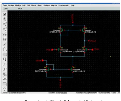
[image:2.612.330.542.218.394.2]Analog design[5] is a fundamentally different discipline to digital logic design. Primarily, it is an optimization problem with a designer altering sizes and positions of circuit elements to ensure that important parameters meet specification, while simultaneously attempting to get the best possible results on other parameters. This results in the notion of correctness being much less measureable than in the world of digital logic, with there often being tradeoffs and compromises. In particular, it comes as a surprise to many digital verifiers to learn that certain parameters in the specification of an analog circuit are only defined after design, manufacture and measurement.
Figure 1. A Circuit Schematic (Cadence)
The process of designing an analog circuit usually follows the following steps.
A. Select an appropriate topology
For the given class of circuit (e.g. amplifier, oscillator, Phase Locked Loop, Digital to Analog Convertors, Analog to Digital Convertors), there will be many different possible topologies (arrangements of components), each of which will have strengths and weaknesses. The designer’s initial task is to select the topology most likely to be optimal for the most significant parameters (e.g. gain) in the targeted process.
This arrangement of basic components (transistors, resistors, capacitors and inductors), usually represented as a schematic in a schematic capture tool (Fig 1), is the initial starting point for the design. This is often taken from a “text book” or from a prior example of a similar component in an existing design database.
B. Sizing
Often, this is done by hand, with the designer making an educated guess based on experience and “back of the envelope” calculations to get these parameters into the right region.
C. Simulation
In order to verify the correctness of the sizing chosen, the designer will simulate the circuit using a transistor level simulator, like SPICE, in a variety of different ways to produce graphical outputs that allow the designer to examine properties of interest.
The initial analysis done by all simulators is “dc analysis”, done to determine the operating point of the circuit, assuming shorted inductors and open capacitors. This will also give the DC transfer function for the circuit. At this stage, appropriately linearized models for non-linear elements may be computed.
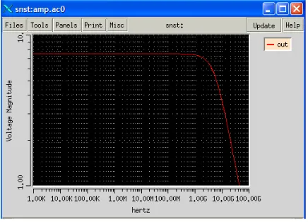
Given this, the next step is usually to perform “ac analysis”. Here, small signal inputs are varied across the frequency range of the circuit, normally providing a frequency domain plot of the transfer function of the circuit. This is the first noticeable difference for people more used to digital logic since the results here are not time based (transient), as is almost always the case for digital devices, but rather is calculated with frequency being the x-axis variable.
More advanced kinds of analysis are also possible, taking advantage of statistical properties of the circuits to find equivalents to steady state and small swing techniques in conditions where they don’t apply directly, such as periodic steady states and stochastic steady states, leading to periodic ac analysis and stochastic steady state analysis.
Finally, in certain cases, it is necessary to examine the behavior of the circuit over time (transient simulation) in a way much more directly analogous to digital simulation with the values of all nodes (more correctly all nodes that are time variant) being calculated to specified time steps. This is generally undesirable since such simulations take a very long time, some times extending over days or even weeks.
The results of these simulations are usually graphical presentations (Fig 2.). The correctness of such results are usually determined by “eyeballing” the graphs, evaluating many parameters simultaneously (“Hmm, that drops off at 10 GHz if Vdd is 1.2 … that’s OK.”)
D. The Design Loop (and Optimization)
[image:3.612.365.583.57.214.2]Often, the simulations serve to illustrate that the desired parameters have not been met and that there is a need to change some of the sizing. This means going back to step B, manually editing the schematic and repeating the simulations. This loop is followed until all the desired properties are met, or more usually, until the most important ones are satisfied and the others are as good as they can be.
Figure 2. Graphical simulation output
There are tools available that can make this iteration process less manual and time consuming. Looking at a couple of illustrative examples of these tools:
• Cadence Neocircuit[6] is a tool that automates the running of simulations, measuring parameters and adjusting sizing until the desired results are achieved. This process is often very time consuming since simulations are run at the transistor level, and there many be a need to run a large number of simulations to get the desired result. The end point (if everything works well) is a circuit with transistors appropriately sized to deliver the performance parameters that were specified in the simulation decks (test descriptions).
• Sabio Labs (now Magma)[7] has a different approach to circuit optimization, in which the circuits are represented by abstract equational models. This allows for much faster simulation and, so faster convergence on the desired solution. The drawback here is that the results are only as good as the model and it can be very difficult to write good equational models for many classes of circuit.
At the end of this iterative process, the designer will have a circuit that is believed to be “correct” i.e. meets the desired performance for the process parameters that were used for
the simulation, which usually means some nominal values that
were selected as representative of the “middle” of the range of possibilities.
E. Verification
to be acceptable whilst the environmental parameters are varied in simulation. Given that most of these values are continuous, or at least are in very large spaces, and that transistor level simulation is very slow, it is even less reasonable to imagine that all such parameters can be simulated exhaustively than in the digital world. Traditionally, the designer’s intuition has been depended upon to select environmental parameters that are likely to have the most effect on the design and to judge when enough simulations have been run to have the required confidence in the design. This is the main reason that analog circuit design and verification is still firmly the domain of experienced designers and has resisted automation much more than its digital cousin.
More recently, simulators such as HSPICE have offered the option of running simulations according to the Monte Carlo approach[8], giving an automated way off allowing statistical distribution of environmental parameters and correlation of results. Whilst this does reduce effort and introduce “randomness” into the simulation choices, it is not as strong a solution as, say, the directed pseudo-random approach to digital verification as there is no formal notion of coverage of the circuit to use as a measure function. In addition, each simulation is still expensive resulting in the entire analysis being very time consuming.
By this point in the design process, the analog circuits are believed to be correct and are offered up for inclusion in the larger chip, which usually includes digital logic. For the purpose of this discussion, we will say that the pure analog design is complete at this point.
III. MIXED MODE DESIGN
In parallel to the process described above, the digital components of the system have been proceeding through a digital design flow, which we will assume is familiar to the audience and will not describe beyond saying that the end result will be
• A collection of High-level Design Language models in some appropriate simulation language (e.g. Verilog[9]) representing the functionality of the digital components
• A collection of layout elements in some format (e.g. GDSII[10]).
These components are assumed to have to interact with the analog components to form a correctly functioning system. As has been shown in other places (e.g. [11]), verifying this is a non-trivial task, requiring the simulation of some components described at the digital level and some that only have meaning at the lower level of transistor analysis. Doing this effectively is still very much an open problem.
A. Mixed Mode Simulation
To date, the industry has offered only one kind of approach to addressing the mixed system verification problem: mixed mode simulation. That is to say, simulation in which some of the components are digital and simulated using, say, Verilog and some are analog and are simulated using, say, SPICE, with the conversion and synchronization between the two domains
being handled automatically. There are many examples of such tools available on the market (e.g. Cadence’s Virtuoso AMS, Synopsys’ Nanosim, Mentor’s ADMS), all having very similar capabilities.
While these simulators offer a huge improvement over the previous approach of synthesizing the digital components and running everything at the transistor level, such simulations are at best a partial solution to the problem since
• They are still very slow compared to digital simulation if there are any transistor level components present.
• At best, they offer a simulation framework. Years of work in the digital domain have shown that simulation is a very weak solution to the verification problem and needs much additional support in order to reach acceptable standards. None of the additional tools (e.g. coverage, static analysis, High-level Verification Languages, formal verification, assertions) are available in the mixed signal space.
B. Verilog (or VHDL)-AMS
Recent attempts to alleviate the problems caused by the large abstraction gap between transistors and digital HDLs have resulted in the creation of analog and mixed signal languages, e.g. Verilog-AMS[12] and VHDL-AMS [13]. These languages combine a digital HDL, an analog language and features for interleaving the two. The AMS languages offer a means of writing more abstract models of analog components and this is a significant step in making simulation of systems involving such components faster. However, whilst there have been a number of approaches to mixed signal verification that make use of such languages, they seem to represent only a small step forward as far as the over all problem is concerned, being just a somewhat more abstract form of mixed mode simulation and so still manifest the problem mentioned above. There are, as yet, no AMS HVLs.
IV. FORMAL VERIFICATION OF ANALOG (AND MIXED MODE)
CIRCUITS AND SYSTEMS
Despite the many years of research in the digital space, there has been relatively little work on applying “formal”1 techniques to analog and mixed signal problems. Part of this seems due to the complexity of the domain (real values, continuous spaces, many dimensional) and part of it seems due to the fact that there is a large communication gap between the (largely digital or theoretical) verifiers and the (largely EE trained) analog designers. In an effort to close this gap, we have recently presented some examples[14] that are extracted from real industrial designs, and so of interest to real analog designers, but are still small enough in scale that they can be used as test cases for academic tools and approaches. This seems to have generated some interest from a number of academic groups and some recent attempts to address one of these examples will be presented below.
1 In this context, meaning mathematically-based, provably complete
XCell1 XCell2 A2
B2
“bridge”
Fi 1 “XCh i OfC ll 2”
XCell1 XCell2
A2
B2
“bridge”
[image:5.612.315.532.51.245.2]Fi 1 “XCh i OfC ll 2”
Figure 3. Even stage Ring Oscillator
Some of the questions that the analog designers are interested in formal verification approaches answering are:
• Will the circuit display correct (acceptable) output behavior for all possible input values (circuit inputs and implicit inputs from the environment)?
• Given that I am happy that the circuit is correct if it is operating near the expected operating point, are the assumptions made about the environment that ensures this operating point reasonable and verifiable?
• What are the ranges of variation of all parameters that the circuit can tolerate and still show correct behavior?
• Is the circuit immune to random initial conditions?
• Are the assumptions across the digital and analog boundaries valid, on both sides, and will incorrect assumptions have been revealed by the verification that has been done?
Understanding exactly where there is value added by using new formal approaches is critical to the successful development of this field since nothing is more useless, from a designer’s point of view, than a different approach that adds nothing and is some times inferior to the existing solution, c.f. the frequency domain analysis vs. transient simulation mentioned above.
A. Examples
As mentioned above, one of the contributions we have been trying to make to the field is to provide some representative examples that are useful for those researchers looking to establish the validity and relevance of their work to analog designers. We will illustrate this with a couple of examples
1) Even Stage Ring Oscillator
[image:5.612.78.280.65.179.2]The first example illustrates some of the peculiarities industrial analog design. The circuit presented is conceptually quite simple: It is a ring oscillator (Fig. 3) intended to produce a regular wave form at a specific frequency (Fig. 4). The natural digital view of such a circuit would be an odd number of invertors arranged in a ring. This example is unusual in that it is composed of an even number of “invertors” together with cross coupled bridge chains. The obvious digital abstraction does not give the right behavior for this circuit. The oscillation is caused by the bridging behavior of the cross coupling invertors and is critically dependent on the relative strengths of the pairs of transistors. There are also ranges of sizes for which
Figure 4. Oscillator Output
the behavior depends critically on the initial conditions of the circuit nodes.
The entire example is composed of 16 transistors, described in 20 lines in a spice netlist
global vdd gnd
.subckt INV in out psource nsource
Mpullup out in psource vdd pch l=lp w=wp Mpulldown out in nsource gnd nch l=ln w=wn .ends INV
.subckt CELL inp inm outp outm
Xinv1 inp outm vdd gnd INV wp='wpchain' wn='wnchain'
Xinv2 inm outp vdd gnd INV wp='wpchain' wn='wnchain'
Xinv3 outp outm vdd gnd INV wp='wpbridge' wn='wnbridge'
Xinv4 outm outp vdd gnd INV wp='wpbridge' wn='wnbridge'
.ends CELL
.subckt CHAINOFCELLS2 ina inb outa outb XCell1 ina inb oa1 ob1 CELL
XCell2 oa1 ob1 outa outb CELL .ends CHAINOFCELLS2
XChainOfCells2 A2 B2 B2 A2 CHAINOFCELLS2
This should be approachable for any reasonable tool but still has sufficient verification challenges to be a good illustration of the value of a proposed approach.
B. PLL
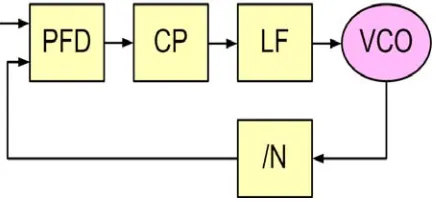
Figure 5. The components of a Phase Locked Loop
This circuit is composed of 5 sub-components:
1. a Phase Frequency Detector;
2. a Charge Pump;
3. a Loop Filter;
4. a Voltage Controlled Oscillator;
5. a divide-by-n.
Essentially, this circuit takes a periodic signal as input and produces, as output of the VCO , a signal that has a different frequency that is phase aligned with the input. In the interest of space, the subcomponents will not be described in detail here but they are all quite straight forward and can be found in any reasonable text book. Interestingly, the PDF and the /N are essentially digital in construction, with the CP and LF being inherently analog.
The interesting thing about a PLL as a verification example, aside from it being a practical application that is found in many designs, is that it has many different failure modes. Most of these failures depend on interactions between the components and can manifest even if each individual component has been verified in isolation. Some examples of observed failures in PLLs are
• VCO doesn’t start
• Output locks to wrong frequency
• Output dithers around locking frequency
Current simulation approaches have been known to miss each of these failure modes on practical examples making this a good candidate for showing the value of novel formal approaches.
C. Formal Verification from the Analog Community
Interestingly, many of the proposed approaches from the formal verification community have not been met with a great deal of enthusiasm from the analog design community. Often this is because the problem being addressed is not one that the design community recognizes as significant. In particular, the approach of transforming a continuous domain into a discrete domain by portioning the space to apply discrete techniques – which is often the obvious approach from the perspective of some one versed in digital techniques – rarely seems interesting to the analog designers.
The reason is obvious once one gets over the fundamental assumption that time based/transient simulation is always the domain of interest. In general, for most analog circuits, there will be some domain in which the circuit will display linear behavior. Indeed, some good analog designers have made the argument that the only way a circuit can ever be really understood is if it has some linear model that can describe the intended function. Given this, forcing the designer to move from a well understood domain that has nice linear properties into a discrete space is not a step forward and so does not get the enthusiasm that the proponent was expecting.
The analog community has offered its own approach to formal verification taking advantage of the presumed linearity.
1) Linear Analysis as an Analog Formal Method
Some recent work from Rambus[15] is predicated on the assumption that, in most cases, a small finite number of parameters are sufficient to completely describe a linear system, and that, in the same way that digital abstraction removes “irrelevant” considerations (such as metastability, delay, noise, etc.) from consideration for digital circuits, the linear idealization of the analog circuit captures the designer’s intent, ignoring unwanted realities (such as distortion or slew rate). Given this assumption, then ac analysis in the voltage or current domains, as provided by say SPICE, is already a complete description of the circuit in the frequency domain, and hence is a “formal method” in the customary usage of the term. So, for any parameter that is represented in the linear abstraction this is a complete solution. The remaining issue for verification is to show that the assumptions are valid.
Further work, as described in [16], allows the extension of these techniques to circuits which are linear on domains other than V or I which are directly supported by the simulators, by providing simple functions that map from the domains which are naturally linear (phase for a PLL, frequency for a VCO, etc.). This allows linear analysis to be the “formal method” for a much wider range of circuits.
This work also serves to point out areas where more “digital” formal methods would have great benefit: These techniques fail if the circuit doesn’t operate at the assumed operating point which allows the linearity assumptions. Formally verifying these assumptions is out of the reach of linear analysis or any other technique currently in use in the analog community.
D. Formal Verification from the FV community
Recently, there have been a number of attempts to apply a variety of formal techniques to some problems in the analog space, with some workshops being devoted to the topic[17, 18]. So far, there seems to be no consensus on the best basis for such an application. In the following section, we present a number of different approaches that have been proposed recently. There are other examples, often by these same groups, but those discussed provide a good introduction to much of the current work in the field.
1) Stability Reasoning
certain classes of start-up error (notably, the complete absence of oscillation) cannot occur. The technique involves solving basic Kirchhoff’s Current Law equations for to identify voltage values for each node in the system, examine the system as a collection of connected paths then perform by a stability analysis to show that the system does not settle to a dc steady state. While this is not a complete proof that the system does oscillate, it is a step in that direction using simple techniques that are easily understood by analog designers and offers good prospects for future tools.
2) Labelled Hybrid Petri Nets and Symbolic Methods
There has been considerable work done at the University of Utah in the area of analog formal verification. One approach use has been to Labeled Hybrid Petri Nets[20] as an intermediate model for translating analog circuits described in VHDL-AMS into a form that can be model-checked using both BDD and SMT based approaches[21]. This has shown some success in finding real issues with small scale analog circuits
3) Discrete Abstraction and Model Checking
A group at the University of Frankfurt has used an approach based on discrete model checking[22], dividing the range of continuous values into discrete states, and model checking properties, described in a custom specification language, over those states. Additionally, recent work has addressed the problem of equivalence checking for analog circuits[23], taking a different branch of the tree that has been followed in the development of practical digital formal tools.
4) iSPICE
Cadence Berkeley Labs has found a way of formulating analog circuit properties as an SMT problem[24], using integer intervals as the underlying theory. This work describes the application of the techniques to a number of examples, including the ring oscillator mentioned above. The work is a very interesting combination of traditional analog work, using simulation to identify values describing intervals and SAT and SMT techniques to then solve properties expressed over these regions. This is early work but looks to hold a lot of promise since it benefits from the significant research happening in the SMT community.
5) Hybrid Automata
A group at Verimag have been working on approaches using hybrid systems techniques to model analog cicuits, extending work on dense time systems to support descriptions using differential algebraic equations[25]. In addition, there has been work on extending assertions into the AMS space, and applying the techniques to practical problems[26].
6) Bond Graph abstraction
A group at Concordia has presented work on abstracting analog circuit properties into bond graphs[27] and expressing interesting properties of the circuits in terms of power flow.
7) Reachibility Analysis
Bruce Krough, Rob Rutenbar of CMU and Goran Frehse of Verimag did some interesting work using forward and backward reachability with iterative refinement[28] to verify some properties of oscillator circuits.
V. SUMMARY, CONCLUSIONS AND OPPORTUNITIES
This paper has presented an overview of the way analog and mixed signal design and verification are done in practice today. That served as a starting point to describe, in a survey like manner, some recent work in the area of analog formal verification, both from the analog community itself and from members of the FV community who have been working in this space.
The state of the art with respect to verification of analog and mixed signal systems is somewhat similar to the state of the art in the digital world in the early 90s: Most of the work is done in simulation at the lowest level of abstraction, with the idea of a higher level language to describe these systems just emerging. In the same way that this was the starting point for digital verification to develop: High level Design Languages, High level Verification Languages, Equivalence Checking, Model Checking, Theorem Proving systems with theories and proof systems for digital hardware, Coverage, Static Timing Analysis, Directed Pseudo-Random test benches, Intelligent Test Benches, etc., we postulate that there is great opportunity to advance the practices in the analog space in similar manners.
Recently, much attention has been given to the significance of analog issues (e.g. [29]). As this paper has shown, while there is exciting work going on in this field, it is far from a solved problem and there are many opportunities for those with formal backgrounds to find problems that are amenable to the tools and techniques they can bring to the table. Hopefully, the introduction to the way analog design and verification is done in practice today, will serve to help such researchers avoid addressing the wrong problems and will serve to bridge the gap between the two communities.
VI. ACKNOWLEDGMENT
As this is a tutorial and a survey of existing work in the field, almost all of the work described here belongs to other people. In addition to thanking the authors of the referenced work, I would like to particularly acknowledge the help of Jaeha Kim, Aida Varzaghani, Metha Jeeradit, Tom Sheffler, Katy Mossawir and Victor Konrad of the Advanced Tools and Methods Group at Rambus, for their contributions to getting analog designers and verification experts to work collaboratively. The presenters at and the program committee of the recent workshop on Formal Verification of Analog Circuits (FAC08) provided much of the information contained herein and their contributions to this paper and to the forming discipline of formal verification of analog circuits is also gratefully acknowledged.
VII. REFERENCES [1] Collet International Research, Survey, 2002
[2] Mandayam K. Srivas and Albert John Camilleri (eds), FM-CAD 1996, Palo Alto, California, Springer (LNCS 1166)
[3] Nagel, L. W, and Pederson, D. O., SPICE (Simulation Program with Integrated Circuit Emphasis), Memorandum No. ERL-M382, University of California, Berkeley, Apr. 1973.
[5] B. Razavi, Design of Analog CMOS Integrated Circuits, McGrawHill, Aug. 2000
[6] Neocircuit Datasheet, Cadence Design Systems Inc, San Jose, CA [7] Sabio Labs (now Magma Design Automation), Mountain View, CA [8] N. Metropolis and S. Ulam, "The Monte Carlo Method", Journal of the
American Statistical Association, volume 44, number 247, pp. 335–341 (1949)
[9] IEEE Std p1364-2005, IEEE Standard Hardware Description Language Based on the Verilog® Hardware Description Language. The Institute of Electrical and Electronics Engineers, Inc. 345 East 47th Street, New York, NY 10017-2394, USA.
[10] Clein, Dan. CMOS IC Layout. Newnes, 2000
[11] Thomas Sheffler, Kathryn Mossawir, Kevin Jones, PHY Verification – What’s Missing?, DVCon, 2007
[12] Verilog-AMS Language Reference Manual, Accellera.
[13] IEEE Std p1075.1, IEEE Standard VHDL Analog and Mixed-signal Extensions. The Institute of Electrical and Electronics Engineers, Inc. 345 East 47th Street, New York, NY 10017-2394, USA.
[14] Kevin Jones, Jaeha Kim, Victor Konrad, Some “Real World” Problems in the Analog and Mixed Signal Domains, Proc of Designing Correct Circuits, 2008
[15] Jaeha Kim, The forgotten Art of Linear Analysis, Invited Tutorial, DAC 2008
[16] Jaeha Kim, Kevin Jones, Mark Horowitz, Variable Domain Transformation for Linear PAC Analysis of Mixed-Signal Systems, ICCAD 2007
[17] Workshop on the Formal Verification of Analog Circuits, ETAPS 2005. [18] Workshop on the Formal Verification of Analog Circuits, CAV 2008
[19] Mark R. Greenstreet, Suwen Yang, Verifying the start-up conditions for a Ring Oscillator, GLSVLSI, 2008
[20] S. Little, N. Seegmiller, D. Walters, C. J. Myers, T. Yondeda, Verification of analog/mixed signal circuits using labeled hybrid petri nets, Proc of ICCAD, 2006
[21] D. Walter, S. Little, C. Myers, Bounded Model Checking of analog and Mixed signal circuits using an SMT solver, Proc. of ATVA, 2007 [22] W. Hartong, L. Hedrich, E. Barke, Model Checking Algorithms for
analog verification, Proc. of DAC, 2002
[23] Lars Hedrich,Sebastian Steinhorst, Structural Methods for Equivalence Checking of Analog Circuits with Strong Nonlinearities, Proc. of FAC 08, 2008
[24] Saurabh K Tiwary, Anubhav Gupta, Joel R Phillips, Claudio Pinello, Radu Zlatanovici, iSpice: A Boolean Satisfiability Based Approach to Formally Verifying Analog Circuits, in Proc. of FAC 08, 2008
[25] T. Dang, A. Donze, O. Maler, Verification of analog and mixed signal circuits using hybrid systems techniques, Proc. of FMCAD 2004 [26] Kevin D. Jones,Victor Konrad, Dejan Nickovic, Analog Property
Checkers: A DDR2 Case Study, Proc. of FAC08, 2008
[27] William Denman, Mohamed H. Zaki, Sofi`ene Tahar, A Bond Graph Approach for the Constraint based Verification of Analog Circuits, in Proc. of FAC 08, 2008
[28] Goran Frehse, Bruce Krogh, Rob Rutenbar, Verifying Analog Oscillator Circuits using forward/backward abstraction refinement, Proc. of DATE 2006