by
• Mohd Alauddin Bin Mohd Ali B.E., BeSC.
2,vvrol led c AI Moot kwokcA )
submitted in fulfilment of the requirements for the degree of Master of Engineering Science
UNIVERSITY OF TASMANIA
•
HOBART
•
•April 1983' .
ACKNOWLEDGEMENTS
This work was carried out in the Electrical Engineering
Department of the University of Tasmania. The author wishes to
thank all members of the staff of the above Department for
their help and cooperation. In particular
,the author
expresses his sincere appreciation to Mr, John Brodie, his
supervisor, for guidance and encouragement in the work,
Acknowledgements are also given to the Public Service
Department of Malaysia for its sponsorship and'the National
University of Malaysia for ittli study leave award.
In the preparation of this thesis, the author thanks
Mrs, Valerie Thomas for her perseverance with the typing and
Mr, Tajul Hashim for drawing the figures.
I hereby declare, that, except as stated herein, this
thesis Contains no material which has been accepted for the
award of any other degree or diploma in any university, and
that, to the best of my knowledge and belief, this thesis
contains no copy or paraphrase of material previously
published or written by another person except Where due
reference is made in the text of the thesis,
_
The switched-capacitor (SC) technique is a very attractive method for implementing fully integrated filters in MOS technology.. The filters, consisting only of switches, capacitors and operational amplifiers, can be realised through a nutter of design procedures. This thesis describes these design techniques and their applications.
Many of the suitable designs use SC integrators which can be easily derived from the analogue active integrators. Parasitic-insensitive implementation is possible realising either the lossless discrete integrator
(Lza)
or the bilinear transformation. The effects of noise and other non-idealities of the switches and operational amplifiers on these integrators are described. A general biquadratic structure based on the SC integrators is given from which a circuit capable of realising bandpass transfer functions is derived. The SC biquads are cascaded orcoupled for the design of higher order filters.
Higher order SC filters are also designed by simulating doubly-terminated 'LC ladder networks with integrators using the LDI
transformation. Other methods of simulating the ladder network include using voltage-controlled current sources, the impedance simulation method and voltage inverter switches. These methods mostly produce circuits which are sensitive to parasitic capacitances and are only briefly described.
These design techniques are used to design SC filters which meet the one-third octave bandpeds filter specification required for the analysis of acoustic noiii and vibration. The midband frequencies of
the resulting SC bandpass filters can be varied from 10Hz to 20kHz. The designs are made using clock frequency at a minimum value possible and another at 48 times the midband frequency. The suitable circuits are compared with regard to their requirements and performances.
The antialiasing problem due to the wide range of required midband frequencies is overcome with the use of an SC decimator circuit. This allows the antialiasing filter, the decimator and other accessories to
be implemented on 4 single Chip with the SC bandpass filter.
The SC circuits are analysed using their z-transform relations. The nodal analysis technique and the equivalent circuit method are described and used for deriving z-transform transfer functions of the SC filters. These are then used to predict the frequency responses of the filters and their sensitivity as to variation of one single capacitor value.
CHAPTER ONE
INTRODUCTION
1
1,1 Switched-capacitor circuit principle
3
1,2 Properties of MOS components
6
1,3 Practical considerations for MOS implementation
9
1,4 Further considerations in designing
switched capacitor filters
11
REFERENCES
13
CHAPTER TWO
ANALYSIS OF SWITCHED-CAPACITOR NETWORKS
15
21 Analysis techniques
16
2„2. Nodal analysis technique
21
2,3 Equivalent circuit method
25
2,4 Examples
31
REFERENCES
36
CHAPTER THREE
SWITCHED-CAPACITOR INTEGRATORS
37
3.1 Transfer fUnCtions
37
3,2 EffectS of parasitic capacitances
42
3.3
Frequency limitations
45
3,4 Noise considerations
51
3.5
Damped Switched-capacitor integrators
54
3.6
Summary
61
CHAPTER FOUR
DESIGN OF SWITCHED-CAPACITOR BANDPASS FILTER
64
4,1 Specification of the bandpass filter
64
4,2 Transfer function satisfying the specification
66
4.3 Transfer function satisfying the
bilinearly-prowarped specification
69
4.4
Transfer function satisfying the LDI-
prewarped specification
71
4,5 Ladder network satisfying the specification
73
REFERENCES
74
CHAPTER FIVE
SWITCHED-CAPACITOR BIQUADS
75
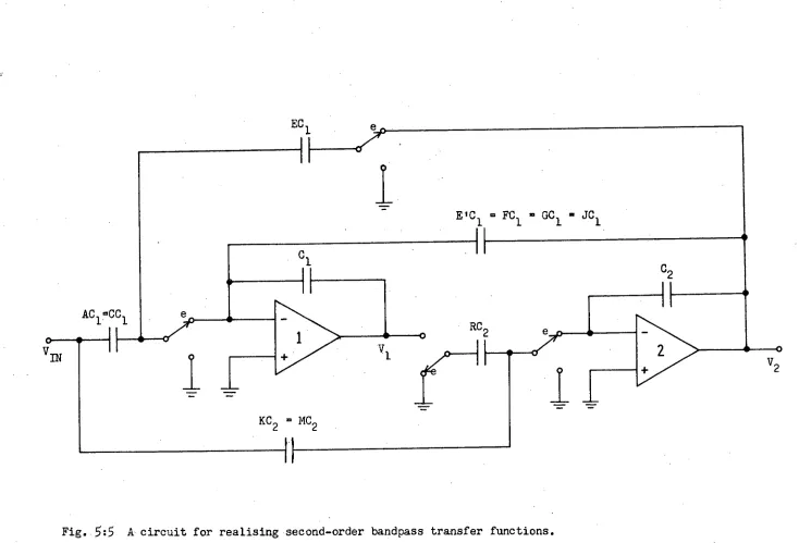
5.1 General biquadratic structure
76
5.2 Transfer functions of the general biquad 82
5.3
Derivation from the general biquad
85
5,4 Design using the bilinear transformation 8 9
5.5
Design by matching transfer functions
91
5,6 Design example using the bilinear transformation 92
5.7
Realising sections with optimum pole-zero
pairing
98
5,8 Design examples by matching transfer functions 101
5.9
Summary
105
REFERENCES
108
CHAPTER SIX
SWITCHED-CAPACITOR LADDER FILTERS
109
6,1 Design using LDI transformation
109
6,3 Minimising distortion by using complex
conjugate terminations
116
6.4
Minimising distortion by
usingbilinear
terminations
116
6,5 Design examples
117
6.6
Coupled-biquad structures from bypass prototype 121
6,7 Coupled-biquad structures from bandpass
prototype
126
REFERENCES
129
CHAPTER SEVEN
FURTHER APPROACHES FOR SWITCHED-CAPACITOR
LADDER REALISATIONS
130
7.1 Using voltage-controlled current sources
130
7.2 Switched-capacitor OTOB realisation
usingVCCS
135
7.3
Using scaled VCCS
137
7,4 Using impedance simulation method
141
7.5
Using voltage inverter switches
147
7,6 Summary
153
REFERENCES
154
CHAPTER EIGHT
IMPLEMENTATION OF SWITCHED-CAPACITOR FILTERS
156
8,1 Antialiasing and smoothing filters
156
8.2 Requirements on the MOS components
162
8,3 Requirements of OTOB filter realisations
163
8.4
Performance of SC OTOB filter
165
8,5 Conclusion
168REFERENCES
170 •
APPENDIX A
Transfer Function of Switched-Capacitor
.Integrator with Finite Operational Amplifier
Bandwidth
171
BIBLIOGRAPHY
175Filters for frequency selective filtering are among the most common circuits in electronic systems. With the advent of integrated circuit. technology, it has also been desirable to produce filters in monolithic form. Towards this end, filters have been successfully reduced in size and cost with the replacement of RLC networks by active-RC circuits.
Avoiding the bulky and costly inductors, thin-film resistors and capacitors can be realised with silicon integrated circuit operational amplifiers.
This hybrid integrated circuit can be fitted into a small 16-pin dual-in-line package.
Further reduction by realising resistors and capacitors on the silicon chip together With the operational amplifier (OA) transistors has been
found to be unsuitable for implementing Precision filters. In order to define accurately the RC product, the absolute values of R and C have to be well controlled which are difficult in current integrated circuit (IC). technology. Integrated resistors have poor linearity and temperature characteristics and they do not track with those of the capacitors on the same chip. However, tracking in variations of the same components allows the possibility of defining resistor or capacitor ratios accurately. Active-R filters have been Implemented, - which use the OA as integrators with their filter parameters established via resistor ratios.[1]
with capacitors, provide a better possibility for full integration of analogue filters. [2]
Another approach for full integration of filters has also been possible due to accurate capacitor ratios and another unique property of MOS IC. The MOS IC offers the ability to store charge on a node for several milliseconds and to sense this stored charge continuously and non-destructively. This feature enables the implementation of analogue sampled-data filters such as the bucket brigade filters [3], the charge-coupled device (CCD) filters [4], the direct-form recursive. filters [5] and the switched-capacitor filters (SCFs).[6]
Thus a number of ways have been attempted for the reduction in size and cost of filters. Among these, the switched-capacitor (SC) technique seems to be the most attractive for the implementation of precise fully integrated filters especially in the voice-frequency range. The SCF
consists only of capacitors, 0As and analogue switches which are all easily implemented in MOS IC. The filter parameters are determined by capacitor ratios and the frequency at which the switches are clocked. The input signal to the SCF is sampled in time thus it should be bandlimited as dictated
by the sampling theorem. Hence an antialiasing filter is required. However, a simple continuous-time filter with no stringent requirement can be easily implemented on the same chip and is usually sufficient for this purpose.
. speech and music synthesisers, can also be easily implemented due to the filter parameter dependence only on capacitor ratios and clock frequency. (9]
The parameter dependence on the clock frequency allows the possibility of implementing an integrated bandpass filter with fixed capacitor ratios but having its centre frequency tracking the clock
frequency. This SC bandpass filter may then be used in applications such as in acoustic noise measurement which involves measuring the level of noise components in different bands of the audio spectrum. [10] The different filters required from the set are obtained by only adjusting the clock frequency of the SC bandpass filter instead of altering the component values as had to be done when using active-RC filters.
• This thesis describes the development in SCF designs, their
advantages and limitations when compared to active-RC filters or other ways of implementing monolithic filters. A number of techniques have been proposed for the design of SCFs.[11] These techniques are described and applied here for the design of the bandpass filter required for acoustic noise measurement. The requirements and performance of the resulting SCFs are then compared to determine their suitability for integrated circuit implementation.
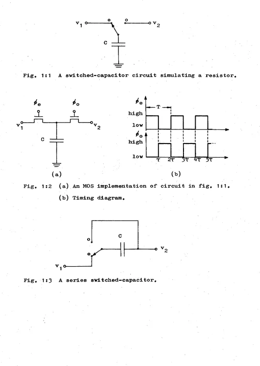
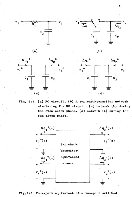
1.1 Switched-capacitor circuit principle
on rapidly switched capacitors. This can be illustrated by the switched-capacitor circuit in fig. 1:1.
Assume the switch is initially at position e,then the capacitor C is charged to voltage vl . When the switch is thrown to position o, the capacitor C is discharged (or charged) to voltage v 2 . The amount of
charge that flows into (or from) the voltage source v 2 is C(vi - v2).
If the switch is thrown back and forth every T seconds, then the current flow, on the average, is
i = C(vi - T
If the switching rate, f c = 1 / T is much larger than the signal ,
frequencies of interest, the sampling time of the signal which occurs in the circuit of fig. 1:1 can be ignored, thus the circuit is equivalent to a resistor of value
R = T/ c = 1 /
(fcC) (1:2)
The MOS implementation of the SC circuit in fig. 1:1 is given in fig. 1:2(a). The two MOSFETs are operated as ideal switches which are controlled by a two-phase non-overlapping clock at the frequency, fc as shown in fig. 1:2(b). The even (e) and odd (o) clock phases, denoted by (0e and 00 respectively, close the switches when they are high. In practice, slightly less than 50% duty cycle is required to ensure the two switches never close simultaneously. However, for simplicity, 50% duty cycle is assumed in subsequent analyses of biphase SCFs.
The SC circuit shown in fig. 1:3 also simulates a resistor as in (1:2).
These circuits can thus replace resistors in any active-RC filters to form
the SCFs if the assumptions in the above illustration are all satisfied. [121 [13]
v 1
v 2
[image:13.568.27.564.60.815.2]C 1
Fig, 1:1 A switched-capacitor circuit simulating a resistor.
Se 00 Oe
high
„J-71____
01
v2
v
.1
low
Olo
1 1 1 1 1 11 i 1 I I 1 i C
-1-
high
low --F—'
T T 1 1
---- : 1 I
(a) (b)
Fig, 1:2 (a) An MOS implementation of circuit in fig. 1:1. (b) Timing diagram.
Inductors can also be simulated using the simulated resistors, capacitors and 0As, hence passive filter response can also be obtained by an SCF.
There are, however, a number of other considerations to be taken into
account to ensure that high performance filters are achieved. These are discussed in detail in the following sections.
1.2 Properties of MOS components
As have been mentioned, it is relatively easy to implement capacitors, switches and 0As in the MOS technology. These high tluality,MOS elements have made the implementation of precise SCF possible. However certain
properties of these components do impose some limitations on the range of realisable filters. In this section the properties of these components, produced through the CMOS or NMOS processes, are described.
(a) MOS capacitors
In the NMOS and CMOS processes, capacitor plates can be made of metal (usually aluminium), or polycrystalline silicon (polysilicon), or heavily-doped crystalline silicon. For examples, a heavily heavily-doped region in the
silicon substrate can be made the bottom plate with the interconnect
metallisation made the top plate or both plates can be formed by two
polysilicon layers. These materials are very conductive. The dielectric material is Si02, an excellent insulator, which can be thermally grown from the silicon layer. These capacitors exhibit good ratio accuracy and low voltage and temperature coefficients.
The value of the capacitors is determined by the dielectric constant, the thickness of the dielectric and the area of the capacitor. Assuming
integrated circuit.
Error in the ratio can thus result from uncertainties in the
photolithographic edge definition. The possible variation of the dielectric thickness with distance across the integrated circuit can also contribute to errors. These effects can be overcome by careful layout of the components. The errors generally get smaller as the capacitor dimensions are made
larger. The achievable ratio accuracies range from 1 - 2% for small capacitor geometries (- 400pm2) to about 0.1% for capacitor geometries which approach the limit of economical size (40,000pm 2).[6] This implies that as the capacitor ratio increases the accuracy decreases since the smaller of the two capacitors must be decreasing.
Voltage coefficients of MOS capacitors are in the range of 10 to 100 ppm/V. Temperature coefficients are generally in the range of 20 to 50 ppm/0C. These variations are much lower for the value of a ratio and
can be considered insignificant in almost all applications.
The manner in which the capacitor is constructed, As described above, renders parasitic capacitance unavoidable. The bottom plate, which is in the substrate or close to it, is coupled to the substrate by a parasitic capacitance with a value of 5 to 20% of the MOS capacitor itself. The interconnecting lines connected to the top plate causes a parasitic
capacitance to be present from the top plate to the substrate. This has a value ranging from 0,1 to 5% of the capacitor. Hence sizeable parasitic
(b) MOS switches
The MOS transistors can operate as good switches. When the transistor is in the off-mode, the off-resistance is, for practical purposes, infinite. The on-resistance depends on the area allowed for the MOS transistor. In NMOS silicon gate technology, switch device with a channel length of 5pm
can be achieved. In this case, for a width-to-length ratio of unity, the on-resistance is 5k0 if the gate drive voltage is 5V with respect to the
source. However, in a larger area,
an
on-resistance can readily beattained.
The 5pm device has a leakage current from source and drain to substrate on the order of 10 -14A at 70 0 C. The parasitic capacitances from source
and drain to substrate is about 0.020pF each. The overlap capacitance from drain to gate and source to gate is about 0.005pF. The charge induced in the channel, When the gate potential is 5V more positive than the source and drain, is approximately 0.03pC.[6] These properties need to be considered in applications where the switches cannot be assumed ideal.
(c) MOS operational amplifiers
The recent trend towards higher level of integration on MOS Large Scale Integration (LSI) chips has led to considerable works being done in realising CMOS and NMOS 0As. A number of high performance 0As have been designed to date. Operational Amplifiers with up to 90dB Open loop gain, unity-gain bandwidth of 10MHz or power dissipation of 2mW are now practical.
[11][17]
have 0.1% settling time of about 2ps for 1 V step with a 20 pF load
and slew rate of about 3V/ps.[14][15] MOS 0As have higher offset voltage and 1 /f noise than bipolar 0As. The MOS OA dc offset is usually less than 15mv. In the overall filter, this adds up according to the filter configuration and the number of 0As used. A typical input noise versus frequency characteristic of an MOS OA is shown in fig. 1:4.[14]
The MOS OA occupies about as much space as a 50pF capacitor, that
is about 0.1 to 0.2 mm2 of silicon area. It does not require large
capacitive and/or resistive loads driving capabilities since 0As used in SCFs are only required to drive small capacitors. Output buffer stage is, however, required for an OA to be used for driving off-chip loads.
1.3 Practical considerations for MOS implementation
The above properties of the MOS elements placed some constraints On the type of SC networks which can be used. A number of circuit conditions have to be avoided in the NOS' implementations of precision filters -. The
guidelines which must be observed for practical SCF configurations are listed below.
(i) Closing the OA feedback path. The OA feedback path should at least
be closed by an unswitdhed capacitor to provide the continuous-time feedback necessary to stabilise the OA. The switched-capacitor alone cannot be used
since the OA will be left open-loop during part of the clock cycle. The switched-capacitor can, however, be used in parallel with the unswitched
10 100 1K 10K 100K FREQUENCY (Hz)
Fig, 1:4 Typical input noise vs frequency characteristic of an MOS Operational amplifier,
10
NOISE (nVil
liz
)
10K
100
accumulation from a variety of parasitic sources. In order to insure stability of the circuit there must be a path either directly or through a switched-capacitor from every node to a voltage source or ground.
(iii) Connection of capacitor bottom plate. This plate should be connected to a voltage source/ground or switched between voltage sources/ground. The large non-linear parasitic capacitance between this plate and the
substrate will then be Charged and discharged, but.will-not affect the filter response.
(iv) Connection of OA positive input. This input should be connected to
a constant voltage. If it is connected to a signal voltage, then the filter response is sensitive to all the parasitic capacitances due to switches, bus lines and substrate that are connected to the negative input of the OA. In addition, increased common-mode performance is required of the OA. [6]
1.4 Further considerations in designing switched-capacitor filters
Despite the above limitations, there are still a variety of possible active filter organisations which can be used for monolithic implementation. These can be arrived at through a number of design procedures starting with an LC ladder or an active-RC filter as a model. These design approaches
and the resulting SC circuits differ widely. Certain practical considerations make Some of these useful networks preferable to others. The features-
listed below are among the considerations which can be used to compare the various - SCF circuits achievable for a particular specification. [16]
(1) The sensitivity of the transfer function to parasitic capacitances.
(2) The sensitivity to changes of the capacitor values, e.g. caused by
12
not be violated if a capacitor value, Cj lies between its upper limit, Cjmax and the lower limit, Cjmin. The value
Cjmax - Cjmin
Cj x 100% (1:3)
is used as a measure of the sensitivity of the filter to deviation of one single-capacitor value.
(3) The total capacitance required which reflects on the substrate
area needed.
(4) The number of 0As in a circuit which determines the power consumption
and the generation of noise. The OA is also a major factor in determining the silicon area required for an SCF.
(5) The spread. of the capacitor values which affect the accuracy of
capacitor ratio definition in monolithic implementation.
(6) The number of switches.
(7) The number of clock phases required.
(8) The allowable clock. frequencies.
Prior to designing the filters, chapter 2 gives two basic analysis techniques which can be used for obtaining z-transform transfer functions of the SCFs. Chapter 3 deals with the SC integrators which are used in
many realisable SCFs. Then the specification for the one-third octave
bandpass filter is given with some preliminary design steps in chapter 4. Using this specification, SCF designs using SC biquads are done in
. chapter 5. Designs by simulating the doubly terminated LC ladder networks . are done in chapters 6 and 7. Finally, in chapter 8, some aspects for
[1] K. Radhakrishna Rao, S. Srinivasan, "Low-Sensitivity Active Filters using the Operational Amplifier Pole",
IEEE Trans. Circuits *.Sst.,
1974, Vol: CAS-21, pp.260-262.[2] R. Schaumann, J.R. Brand, "Integrable analogue active filters for implementation in MOS Technology",
IEE P1ioc.,
1981, Vol. 128, Pt. G, pp.19-24.•
[3]
F.L.J. Sangster, "The Bucket Brigade Delay Line, a Shift Registerfor analogue signals",
Philips Tech. Rev.,
1970, Vol. 31, pp.97-110. [4] D.D. Buss, D.R. Collins, W.H. Bailey, C.R. Reeves, "TransversalFiltering using Charge Transfer Devices",
IEEE J. Solid State
Circuits,
1973, Vol. SC-8, pp.138-146.[51
I.A. Young, D.A. Hodges, "MOS Switched-Capacitor Analog Sampled- Data Direct Form Recursive Filters",ibid.,
1979, Vol. SC-14, pp.IO20-1033.[6] R.W. Brodersen, P.R. Gray, D.A. Hodges, "MOS Switched-Capacitor Filters",
PI.oc. IEEE,
1979, Vol. 67, pp.61 -75.[7] K. Yamakido, T. Suzuki, H. Shirasu, M. Tanaka, K. Yasunari, J. Sakaguchi, S. Hagiwara, "A Single-Chip CMOS Filter/Codec",
IEEE J. Solid
-State Circuits,
1981, Vol. SC-16, pp.302-307. [8] B.J. White, G.M. Jacobs, G.T. Landsburg, "A Monolithic Dual ToneMultifrequency Receiver", ibid.1979, Vol, SC-14, pp.991 -997.
[9] D.B. Cox, L.T. Lin, R.S. Florek, H.F. Tseng, "A real-time Programmable switched-capacitor Filter",
ibid.,
1980, Vol. SC-15, pp.972-977.[10] P.J. Yates, "An Investigation into the suitability of using ,a switched-capacitor filter to form a one-third octave B.P. filter with a variable centre frequency", Honours Thesis, Elect. Eng. Dept.,
University of Tasmania, 1981.
[11] G.C. Temes, "MDS Switched-Capacitor Filters-History and the State of the Art",
Plioc.,
1981 European Conf. on Circuit Theory and Design, pp.176-185.[12] L.P. Huelsman, P.E. Allen,
Introduction to the Theory and Esign of
Active Filters,
New York, USA: McGraw-Hill, Inc., 1980.[13] M.E. Van.Valkenburg,
Analog Filter 16sign,
New York, USA: Holt, Rinehart and Winston, 1982.14
[15] A. Iwata, K. Uchimura, S. Hattori, H. Shimizu, K. Ogasawara,
"Low Power PCM CODEC and Filter System",
ibid.,
1981, Vol. SC-16,pp.73-79.
[16] E. Luder, G. Spahlinger, "Performance of various types of
Switched-Capacitor Filters",
Arch. Elektron. Vebertr.,
1982, Vol. 36,pp.57-62.
[17] T. Ishihara, T. Enomoto, M. Yasumoto, T. Aizawa, "High-speed NMOS
Operational Amplifier Fabricated using VLSI Technology",
Electron.
In chapter one, it was shown that a switched-capacitor can approximate a resistor under the assumptions that the sampling frequency is much greater than the signal frequencies and that the resistor is voltage
driven at both ends. In this case, the SCF can be considered equivalent
to the active-RC filter it replaces and analysed as such. However, such assumptions are not always practical in the analysis of SC networks. For example, it is desirable for the signal frequencies to be as high as half
the sampling frequency, thus the time delay through the switched capacitor has to be accounted for.
A more exact analysis can be obtained by applying the z-transform techniques, if the voltage sources and internal voltages of the SC networks are assumed to be sampled at times kr (where k is an integer, see fig. 1:2(b)) and held over one-half clock period. The resistor/switched-capacitor
correspondence is still useful for deriving topologies of SC networks from the active-RC circuits. Then the SC networks are considered to be pure sampled-data systems and analysed using the z-transform techniques. For this analysis to be exact, the SCF has to be preceded by a sample-and-hold (S/H) stage. However, in many SC networks, this is not necessary since the S/H operations are inherently performed by the SCF.
Without the above assumptions, the SC networks can still be analysed for arbitrary input signals and arbitrary switching patterns where both frequency domain and time domain information can be derived. [1] The analysis, however, is considerably more complex. For convenience or for practical reasons, most SC networkdesigns are based on S/H input signal.
16
Thus this chapter only deals with the analysis of biphase SC network assuming sampled-and-held inputs. For this class of circuits, simple and fast analysis techniques are available but they only provide for the analytical evaluation of transfer functions and frequency responses of the SC circuits.
2.1 Analysis Techniques
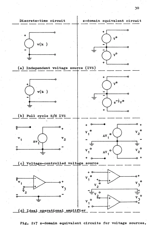
The use of the z-transform in the analysis of SC network is first illustrated here for the SC circuit in fig. 2:1(b) which corresponds to the simple RC circuit of fig. 2:1(a). The resistor of the RC circuit is replaced by the switched-capacitor of fig. 1:1. The SC circuit is assumed to comprise of ideal switches and capacitors. The switches are controlled by clock phases as shown in fig. 1:2(b).
The topology of the SC network is thus changed periodically between two states as shown in fig. 2:1(c) and (d). The port variables can be characterised in terns of discrete time voltages, v x (kT) and discrete time
- charge variation, Aq x (kT), where x represents nodes in the circuit. At
the switching time, ler when k is even, the SC network becomes that of fig. 2:1(c), and charges are instantaneously redistributed with the principle of charge conservation maintained At every node. Using this prinCiple, nodal charge equations can be written at each node for the even sampling instants. These are
Aqie(ler) = ivie(kT) - C 1v 20[(k -1)T] (2:1a)
Aq 2e(kT) = C 2v 2e(ler) - C 2v 20[(k -1)T] (2:1b)
-z C 1
-z-4 C2
v
1
V 2
e
V1 o
V20
2
(2:3)
Q e
c
i
17
At the switching time, kr, When k is odd, the network becomes that of fig. 2:1(d) and the nodal charge equations for this instant are
Aq ic)(kT) = 0 (2:1c)
°
(kT) = C 1V 20(kT) + C 2v 2 °(kr) - C iv ie[(k - 1)T] - C 2v 2e[(k - 1)T](2:1d)
Applying the z-transform, where z = exp(sT) in which s is the complex analogue frequency variable and T = 2T, eqns (2:1) becomes
AQ1e(
z
)
=ci
le(z)
z-1C 1V2 °(z)
(2: 2a)AQ 2e (z) = c 2v2e (z) - z- /c 2v2
(z) (2:2h)AQ 1°(z) = 0 (2:2c)
C 1V 20(z) + C 2V20(z) - z C i Vie(z) -
2V2e(z) (2:2d)
where AQ(z) and V(z) are z-transforms of Aq(kT) and v(kT) respectively.
Thus at a particular node of the SC network
of
fig. 2:1(b), twodistinct, but coupled, nodal charge equations are required to characterise
the charge conservation. Eqn . (2:2) can be written in matrix form as
follows
The transfer functions describing the circuit can be obtained from
(2:3) using cofactor techniques. Let
pa
represent the matrix, these18
-0v 2 R
1
C 2
(a)
(b
)A 0
1
C2
( c)
(a)
Fig. 2:1 (a) RC circuit. (b) A switched-capacitor network simulating the RC circuit. (c) network (b) during the even clock phase. (d) network (b) during the odd clock phase.
4. Agle(z)
—>
0
Q2 e( z )
'
v
1
e
(z) •••-->
+ 0
"'
Switched-capacitor equivalent network
V e(z) 2
A n
o tz ) ‘2v 20( z)
[image:26.565.21.528.22.779.2]V
2 .
1 Y121
v _ C l zV 1 1'111 C
1 + C2 -,
c
2
z-1e
-t
✓ o
1Y141
C 1
z
eo 2 = =
1'1111 +C -Cz -1
H = V 1
e
1 2 2
✓
e
Hoe = 2. = 0
✓ 11331
V
-oo
H = • 2 _Ld - 0
V
1° 1Y331
(2:4a) (2:4b) (2:4c) (2:4d) The relation, where SC network
V2e(z)
V
2°(z)
[ V 1(z) V 2(z) = V 1
is thus fully
Hee Hoe
Heo H°
e
(z) + V10(z)
e
(z) + V 20(z)characterised
V
1e(z)
V
1°(z)
by
the input-output(2:5a)
(2:5b)
(2:5c)
The SC network can then also be represented by an equivalent four-port as shown in fig. 2:2 where the equivalent z-domain network is described by (2:5a) or (2:3).
Signal conditioning performed at the input and output determines the relevant transfer function relations of the SC network. As an example, if the output is sampled only at the even la time instants, then the
relevant relation is
v 2e e f Hee
v1 e
tzl H oe v1e o f
20
In the circuit of fig. 2:1(b), however, the input at the odd kt time instants is not sampled, thus for this case only the transfer function
Hee is involved.
If a general SC network is now considered, the two z-transformed nodal charge equations at a particular node x are written as
Nex Nex
texfzi E ne f t .% z- 2 E Qox (z)
/
j=1 No Nox Q°(z)
E
Q°(z) _ z-i E- ex.(z)
j=1 j=1 I
2:7a)
(2:7b)
where Nex, Nox denote the total number of capacitors connected to node x
during the even and odd clock phases respectively. Qexi(z), Q° (z)
are z-transforms of the instantaneous charges stored on the j-th capacitor connected to node x at the even and odd kt time instants respectively.
As the circuit increases in complexity, it becomes very difficult to write dawn (2:7). The transfer functions as in (2:5a) can no longer be easily obtained as for the case of the simple circuit of fig. 2:1(b). • A number of analysis techniques have been proposed which simplify these
steps. The following sections deal with two basic methods which Are capable of handling any two-phase SC network containing ideal elements with S/H inputs. These are the nodal analysis technique [2] and the equivalent circuit method. [8] Based on these, more general methods have been
c
1
0 0 C
2 0
[C] =
0 •0
(2:8) 2.2 Nodal Analysis Technique
Using (2:7), the total number of equations involved to describe a SC network is 2n, where n is the number of nodes in the network. In
this nodal analysis technique, the network is broken down into switches and capacitors networks. Using matrices which describe these networks, equations such as in (2:7) can be assembled in a logical manner. . This method is particularly attractive for computer analysis of SC networks.
In this analysis, it is first assumed that any branch between two nodes in the network consists only of a.capacitor and a switch. Thus another node has to be introduced for the circuit of fig. 2:1(b) for its analysis using this method. The circuit is redrawn in fig. 2:3 broken down into its switches and capacitors networks with the nodes renumbered.
this way, the same capacitors are connected to each node at all time instants. Thus, from fig. 2:3(b), a fixed capacitance matrix can be written as follows,
The voltage at each node is determined by the switch connection.
Thus when switch e closes, taking V le as the reference in fig. 2:3(a),
V
1 = Vl
e
' , V 3
e
2:9)
22
e_ V
1 V e
2 V 3 e 1 1 1 0 0 0 0 0 0 1 V1 V2 e V3 e
= [Se ]Ve (2:10)
where [Se] is the even switching matrix and ye is the corresponding vector of the voltages at the nodes of the circuit. Similarly, when
'
switch o closes, the switching matrix [S ] can be obtained and the corresponding vector V° defined as
0 0 V
1° = [0 0 1 , Vo V
2 o
(2:11)
0 0 1 V
3 o
Equations such as in (2:7) can then be written in matrix form as follows
FAael . [
N]
[tse] -z-
l[s°1
[ve
Aq
°
[0]
[C] -z-1[Se] [S°1
V°(2:12)
where, due to the different node definition, AQ(z) is now used to denote "e "o
the z- transformed charge variation. AQ and AQ are vectors of the z-transformed charge . variations at nodes of the network when switches e and o close, respectively..
The closing of the switches reduces the actual number of nodes:in the circuit. This has to be taken into account by using the charge
matrices [Ie] and [Io] for the even and odd ki time instants respectively. When witch e closes in fig. 2:3, the actual charge variation at the
2
3
V
1 V 2 2_, V
0 o o 3 (a)
6414' Le124, Q34'
0
I
di(b)
Fig. 2:3 (a) Switches network of the circuit in fig. 2:1(b). (b) Its capacitors network.
°V r
(a)
@ e 0
X r x . r
• • • •
• • • •
• • •
• • •
• • •
•
•
.
•
• I
•
.
a.
•
•
I
•
• •
• •
•
•
•
•
•
•
• • •
(b)
24
e ^ e"ee AQ
1 = AQ1 + AQ2 , AQ 2 = 0 (2:13a) and since switch o is open at this instant,
AQ3
e AQ3e(2:13b)
Similarly
ml
o .These are
Q e
AQ 2e AQ 3e when AQ1 °
60 2
o-4 AQ 3° { _ = . written switch in matrix 1 1 0 0 0 0 0 0 1
o closes, : 0 0
0 1 1
the form
e
- 6'1:1 1 " e AQ 2 " Ai e-_
AQ1o "
An 0 2 ^ 0 AQ 3
matrix as
= [le ] AQ e
equation is
= AQ°
(2:14)
(2:15)
Hence in general, all the nodal charge equations can be assembled In matrix form as follows [2], using (2:12), (2:14) and (2:15);
or
re I re ][c][s e i _ z-i [ e ][c][s olve I _ zl o imis e [ e ][c][s o
] vo
(2:16)
AQ =
['qv
For the circuit of fig. 2:1(b), the same matrix equation as in (2:3) is obtained after elimination of rows and columns of the matrix [Y] which are zero, and their corresponding variables.
nodes x and r. The voltages at the nodes are related by
e V o
V
v e. _ r ,v o. _ r
x A x A (2:17)
o o
The matrix [Y] is shown in fig. 2:4(b) showing only variables, rows and columns of the relevant nodes. Using (2:17), column xe of
the matrix is divided by Ao and subtracted from column re and column xe is discarded. Similar steps are done for columns x° and r0. The rows involving AQer and AQo are also discarded since they express the current outputs from a voltage source and thus are redundant. When A 04 oo for an ideal OA, these steps merely involve discarding columns xe, ,c0 and rows involving AQer, °r [3]
Thus normally the matrix [f] can be reduced to at most a 4 x 4 matrix as in (2:3). If necessary, pivotal condensation can be applied to reduce the matrix. Then, after considering the signal conditioning to the SC network, cofactor techniques are used as before to derive the relevant transfer functions of the network.
This technique can be extended for the analysis of multiphase Sc networks [4] and SC network using amplifier With finite gain and finite bandwidth.[5] Computer programs for the analysis of SC networks based on this technique have been implemented. However, most computer-aided- design (CAD) programs use the more efficient modified nodal analysis (MNA)
techniques for the computation of SC network.[6][7]
2.3 Equivalent Circuit Method
=0
= CV
2e (z) - CV1 e(z) - Cz
+ C z
26
z-transformed nodal charge equations as in (2:7). Any Sc network can then be transformed into a z-domain equivalent circuit by interconnecting the appropriate building blocks. It is then possible to apply familiar network analysis techniques on the SC netWork equivalent circuit to derive the transfer relations between any pair of nodes of the network. This method is appealing from the practical insight view.
The circuit shown in fig. 2:5 is the most general switched . (single) capacitor element. Other SC elements are specific cases of its configuration. Thus only its equivalent circuit needs to be derived directly from the
z-transformed nodal charge equations. By manipulating this equivalent circuit, the other useful SC building blocks can then be derived. These blocks, together with the equivalent circuits for independent and voltage-controlled voltage sources form a library of building blocks which can be used for both the analysis and synthesis of biphase, SC networks.[8][9] This method of analysis has also been extended so that it can be applicable for multiphase SC network [10] and biphase SC network with continuous
input signals, and duty cycle not equal to 50%.[11].
The z -transformed nodal charge equations for the toggle-switched floating fou
AQ1e(z)
AQ1 (3(z)
AQ2e(z)
r-port (TSFFP) in fig. 2:5 can be written as follows = CV
1 e(z) - CV2e (z) - Cz V3
o
+ Cz V 4 o (2:18a) (2:18b) ° (2:18c) (2:18d) AQ3e (z)
,Q30 (z)
AQ4e(z)
4
4°(z)= 0 (2:18e)
- = CV
30 (z) - CV40 (z) -
-I Cz V 1
e
+ Cz IV
2e (2:18f)
=0 (2:18g)
= CV
2
7
Aq1 4 q3
•
---> e 0
0
1
C
o
V3
-
A c1 2
Fig, 2:5 Toggle-switched floating four-port. •8]
28
Equation (2:18) describes an eight-port equivalent circuit with four open ports. These open ports can be deleted and the remaining equations in (2:18) are used to derive the four-port equivalent circuit
shown in fig. 2:6(a) for the TSFFP. Note that the even (e) and odd (o)
phases are interchangeable on the SC circuit, i.e. if the capacitor in
fig. 2:5 is connected to V1 and V 2 during the o phase and to V 3 and V4
during the e phase, then the equivalent circuit is obtained by interchanging the superscripts of the variables of the equivalent circuit in fig. 2:6(a).
The TSFFP is equivalent to the floating capacitor in fig. 2:6(b)
if V 3 = V1 and V4 = V 2 . Thus the equivalent circuit for the floating
capacitor can be derived from that of the TSFFP by making similar
replacement of the subscripts for its variables. The toggle-switched
capacitor of fig. 2:6(c) can be obtained by grounding V 2 and V4 of the
TSFFP. Thus the corresponding equivalent circuit is similarly obtained. The series-switched capacitor of fig. 2:6(d) is obtained by shorting V 3 and V
4 of the TSFFP and its equivalent circuit is as shown. Other SC
z-domain equivalent circuits can similarly be derived.
1
V
(c) Toggle-switched capacitor
v%A.
1
o
+
Ac1 2 +0
2
OM.
2
9
Discrete-time circuit
(a) Toggle-switched .floating four-port
Aqi --›
+0
II
(b) Floating capacitor
1
z-domain equivalent circuit
(d) Series-switched capacitor
? v
1
v 2
0+
V 3
30
Discrete-time circuit z-domain equivalent circuit
(a) Independent voltage source (IVs)
v(k )
(b) Full cycle S/H IVS
v
1 v2
(c)voltage-controlled volt ge source
V
1
o
+ 0
Adildeal operational amplifier v(k )
[image:38.565.34.524.14.762.2]by appropriately interconnecting the blocks in fig. 2:6(b) and (c), and the source in fig. 2:7(a).
2.4 Examples
The SC network shown in fig. 2:8 will be used to further demonstrate the two methods of analyses described. The network is actually a circuit for the switched-capacitor integrator (SCI) as will be shown in chapter 3. The relevant transfer functions as defined in (2:5) for this circuit are . derived.
1. Deriving transfer functions using nodal analysis technique. The circuit in fig. 2:8 has its nodes numbered as shown. The switches and capacitors networks of the circuit can then be drawn
separately as in fig. 2:9. From fig. 2:9(a), the following matrices can be written
[S e = 1
0 0
(s°1=
11 0 0 0 0 1 0
o
0 1 0 0 0 1 0o
0 0 1 0 0 0 1(2:19) [lI = e 1 1 0 0 [I9 = 1 0 0 0
0 0 0 0 0 0 0 0 0 1 0 0 1 1 0 0 0 0 1
I. 0 0 0
From fig. 2:9(b), the capacitor matrix is
(c 1=
0 0 0 00 C
1 0 0 (2:20) 0 0 C
2 -C2 0 0.-c 2 C
32
Fig, 2:8 A switched-capacitor integrator.
V o V
v
4
2
0 0---0
(a)
WI
0
+A Z'l
1if6:43
4(.61
.(
14
2
i
3
C-
It
2 •
1
C
o
i i
Pig, 2:9 (a) Switches network of the switched-capacitor •integrator, (b) Capacitors network of the
switched-capacitor integrator,
0
V e
r -1
•
Heo - l Yi 3 1 -‘1- z (2:23h) Ill,
C
2(1 - z 1 ) 1 33 obtained, - 4 e 1 AQ2e AQ3e 44 o 41 0 42
A 0 4 3 o 44 Putting = (2:19) C
l 0 0
0 0 0
-z-iC 0 1
0 0
and (2:20) in (2:16),
0 0 0 0 0 0 0 0
-C
2 C2 0 0 0 0 0000 -z-IC
2z -IC
2 0 0
Z-IC
2-z
4C 0
the following matrix
-z-iC
l 0 0
-z C
2 C z I C
2 -z I C2 0 0 0 0 C
1+C2 -C2 -C
2 C 2
;1e e V 2 V 3 e V 4 o V 1 V 2 o V 3 o o V 4 equation (2:21)
The zero columns and rows of the matrix in (2:21) can be eliminated. • Also, the presence of the ideal OA between nodes 3 and-4 makes it possible'
to discard columns 3 (even), 3 (odd) and rows 4 (even), 4 (odd). Thus the reduced matrix equation is
is
•
AQie. AQ 3e
AQ3o
Cl 0 0
0 -C 2 -/ -z C
1 z C2 -C2 V 1e e V4 V
4
(2:22)Note that V
1 is absent in (2:22) since the input is only sampled during the even clock phase. The relevant transfer functions of the SCI are
-1
2:23a) Hee V4 =
1
121 . Y -C l z V e I Y111 C
34
2. Deriving transfer functions using equivalent circuit method.
By properly interconnecting the SC building blocks of fig. 2:6(b), (c) and fig. 2:7(a),(d), the SCI in fig. 2:8 is transformed into its
z -domain equivalent circuit shown in fig. 2:10(a). This can be simplified by removing elements shunting virtual ground points and voltage sources.
The simplified circuit is shown in fig. 2:10(b) which can be reconfigured into the circuit in fig. 2:10(c).[8] The relevant transfer functions can then be easily obtained to be
C
1 z-1 V
4 e
H
ee (2:24a)-1
V e C
2(1 - z)
1
C
1 z_i V
4 o
H
eo (2:24b)C2 (1 -
-1
)
Vi
ee - 1 eo
which are the same as in (2:23). Note that H = z H , i.e. the output of the SCI is held over the full clock cycle.
3. Frequency responses
The above z-transform techniques accurately predict the input-output relationship of the SCI on a sample-by-sample basis. The frequency
response on this basis is obtained by setting z = exp(jwT). However, in between these samples, the output of the SCI has the held, staircase-like -wave shape. This analogue character of the circuit can be taken into
account by multiplying the z-transformcomputed frequency response with
(a)
C
1 C
2 —±VV\1"—.
-C
2z -2 C2 •
Ar40
(b)
4
[image:43.567.50.530.58.776.2](c)
36
REFERENCES
[1] Y.P. Tsividis, "Analysis of Switched Capacitive Networks", 1ELE
Trans. Circuits Syst.,
1979, Vol. CAS-26, pp.935-946.[2] C.F. Kurth, G.S. Moschytz, "Nodal Analysis of Switched-Capacitor Networks",
IEEE Trans. Circuits Syst.,
1979, Vol. CAS-26,pp.93-104.
[3] J.I. Sewell, "Analysis of Active Switched-Capacitor Networks",
Proc. inT,
1980, Vol. 68, pp.292 -293.[4] E. Hokenek, G.S. Moschytz, "Analysis of multiphase switched-capacitor (m.s.c.) Networks using the indefinite admittance matrix (i.a.m.)",
IEE
Proc.,
1980, Vol. 127, Pt.G, pp.226-241.[5] J. Lau, J.I. Sewell, "Inclusion of Amplifier Finite Gain and Bandwidth in Analysis of Switched-Capacitor Filters",
Electron.
Lett.,
1980, Vol. 16, pp.462-463.[6] J. Vondewalle, H.J. DeMan, J. Rabaey, "Time, Frequency, and z-Domain Modified Nodal Analysis of Switched-Capacitor Networks",
iEEE Trans.
Circuits Syst.,
1981, Vol. CAS-28, pp.186-195.[7] R. Plodeck, U.W. Brugger, D.C. von Grunigen, G.S. Moschytz, "SCANAL -
A program for the computer-aided analysis of switched-capacitor networks",
IEE Proc.,
1981, Vol. 128, Pt. G, pp.277-285.[8] K.R. Laker, "Equivalent Circuits for the Analysis and Synthesis of Switched Capacitor Networks",
Bell Syst. Tech. J.,
1979, Vol. 58, pp.729-769.[9] F. Anday, "Realization of second-order 'transfer functions with switched-capacitor networks",
Int. J. Electronics,
1981, Vol. 50, pp.169-174.[10] J.J. Mulawka, "By-inspection analysis of switched-capacitor networks",
ibid.,
1980, Vol. 49, pp.359 -373.CHAPTER THREE
SWITCHED-CAPACITOR INTEGRATORS
An attractive technique for the design of switched-capacitor.filters is based on active-RC filters which use integrators as building blocks.
These include state-variable biquadtatic circuits which are used in cascade design and leap-frog filters which simulate the operation of low-sensitivity, doubly-terminated LC ladder networks. The integrators in active-RC filters can simply be replaced by active switched-capacitor integrators (SCIs) such as given in fig. 7:8. The presence of the
operational amplifier in each integrator makes it possible to eliminate effects of paraSitics, thus ensuring accurate and reproducible filters.' These features make the technique a popular approach for SCF design. Thus the SCIs form an important part of many realisable SCFs.
Hence, its development is discussed in detail in the following
sections.
3.1 Transfer Functions
Fig. 3:1(a) shows the conventional analogue integrator with transfer function
H(s) = 1 (3:1)
Ri C2s
Originally, the SCI is developed from the analogue integrator by replacing the resistor with its switched-capacitor equivalent discussed in chapter
1.[1][2] Using the switched-capacitor "resistor" of fig. 1:1, results in
the SCI in fig. 3:1(b) as in fig. 2:8, which has been referred to as the .
toggle-switched integrator. With R1 = li(f c c i). , assuming frequencies
much less than the clock rate, f c , the frequency response of the SCI is given - by, (setting s = jw)
[image:45.567.50.542.27.582.2]H(w) = -
(3:2)38
Using the series switched capacitor in fig. 1:3, the integrator in fig. 3:1(c) is obtained.
Eqn. (3:2) shows that the integrator gain is dependent on a capacitor ratio and the clock frequency. The ability to obtain precise capacitor ratios and a very stable clock means that precision integrator gain can be produced.
However, the actual frequency response of the SCI deviates from that Of the analogue integrator, especially for frequencies approaching the clock frequency. Due to its sampled-data nature, a more exact analysis using z-transform techniques as discussed in chapter 2 has to be used. The transfer function of the SCI when the output is sampled during the even interval is (see eqn. (2:24a))
C
_1
H
ee z-1 (3:3)By setting z = exp(jwT) where T ■ 1/f c , the frequency response is then
given by
H(w) = - f c C l . 1 wT
C 2 1,) e"P -1 .( (3:4)
• 2
2 I
Comparing (3:2) and (3:4), both magnitude and phase deviations are present in the frequency response of the SCI, especially when w'T<<1 is not satisfied. The magnitude deviation is not significant. However, the excess phase shift is important in that it will cause distortion in the form of Q-enhancement in which the response of the complete filter shows some undesired peaking. [3]
V OUT
VIN
V OUT
(a)
( b ) (c)
Fig. 3:1 (a) Analogue integrator. (b) Toggle-switched integrator. (c) Series-switched integrator.
40
implementing the integrator as in fig. 3:1(b) realise the mapping 1 1 - z-1
s (3:5)
z-1
which is the forward difference transformation. This transform the Imaginary axis in the s -plane to the vertical line going through z = 1 in
the z -plane instead of onto the unit circle. Thus it maps high -Q s -plane
poles and zeros into z -plane poles and zeros which are very close to the unit circle or even outside it.
For the integrator in fig. 3:1(c), its transfer functions can be obtained from its equivalent circuit in which blocks of fig. 2:6(b), (d) and fig. 2:7(a), (d) are interconnected. When its output is sampled during
the even interval, the transfer function is,
He - C.1 1
CI 1 - z-1
(3:6)
Comparing (3:1) and (3:6), this implements the backward difference transformation.
(1 - z
-1
).
(3:7)This maps the imaginary axis of the s-plane inside the unit circle of the z-plane.
The excess phase shift in (3:4) can be eliminated if the output is sampled during the odd interval.[4] Hence, as in eqn. (2:24b), the transfer function of the SCI is
Heo _C1. z•i (3:8)
2 1 _ z-1 which gives the frequency response,
H(w) = 1cC1 1 WI •
C2 jw 2sin(aT
- C
3 z-i (V ac) - Vb0) (3:12)
C4 1 - z 1
Thus, if the switch phasing in the overall circuit of the filter ensures that the output of the integrator is sampled correctly, then
the undesirable effects due to the excess phase shift can be avoided. This implementation is equivalent to realising the lossless discrete integrator (LDI) transformation
1
s (3:10)
The LDI transformation, maps the imaginary axis of the s-plane onto the unit circle of the z-plane and ensure stable s-domain transfer •
functions map into stable z-domain transfer functions. The magnitude
deviation as in (3:9) is due to the fact that only the portion - 2 2
of the the imaginary axis of the s-plane is mapped onto the unit circle.
The deviation can thus be adjusted, if necessary, by prewarping the continuous-time filter frequency, using
2
sin (=-ALIT )
2 (3:11)
i.e. by replacing w in (3:2) by Q, (3:2) becomes equivalent to (3:9).
As an example, the two-integrator loop sham in fig. 3:2 has proper witch phasing and thus is free from phase errors. This loop forms an
important section in building switched-capacitor ladder filters .as discussed
in chapter 6. Note that integrator 1
in
fig. '3:2 realises theswitched-capacitor differential integrator, since switched-capacitor C 3 is charged to the
difference between two input voltages, V a and Vb . Using the equivalent
circuit method in chapter
2,
the input-output relation is determined to beFrom (3:12), it can also be noted that integrator 1 in fig. 3:2
42
3.2 Effects of Parasitic Capacitances
• Another deviation of the SCI from ideal behaviour could be contributed.
by parasitic capacitances as shown in fig. 3:3 with the SCI of fig. 3:1(b) drawn in its MOS implementation. The gate-to-diffusion overlap capacitance,'
such as Cgd feeds a portion of the clock signal, (Po onto the output'. The
effect of this feedthrough is to produce a dc offset voltage at the output of the integrator. Self-aligned MOS technologies with small overlap
capacitances can be used to greatly reduce this effect. (5.] Also, if CMOS switches are used, the positive rising, and negative falling edges causing feedthrough are nearly matched and almost exactly cancelled. (6]
Another technique to overcome clock feedthrough is by adding a network to the positive input of the OA to cancel the signal injected by clock feedthrough at the negative terminal. [7] The cancellation, however, is dependent upon matching of the switches involved and assumes infinite common mode rejection ratio (CMRR) of the • OA. besides requiring double the total amount of capacitances.
Parasitic capacitances- Ct2 and Cb2 from the top and bottom plates,
respectively, of the'integrating capacitor C2, have no effect on circuit. operation. This is due to their being Always connected to virtual ground and a voltage source respectively. The top plate of the capacitor, which has lower parasitics, needs to be connected to the negative input of the OA in order not to impose stringent requirement on the OA low frequency
gain.
The parasitic capacitance, Ca, from the top plate of capacitor CI,
includes parasitic capacitances from the source or drain of the switches