REVIEW
Nanostructured thermoelectric materials: Current research
and future challenge
Zhi-Gang Chen
a,, Guang Han
a, Lei Yang
a, Lina Cheng
a, Jin Zou
a,b,a
Materials Engineering, The University of Queensland, St Lucia, QLD 4072, Australia
bCentre for Microscopy and Microanalysis, The University of Queensland, St Lucia, QLD 4072, Australia
Received 18 July 2012; accepted 7 October 2012 Available online 23 December 2012
KEYWORDS
Nanostructured thermoelectric materials Thermoelectrics Power generation
Abstract The field of thermoelectrics has long been recognized as a potentially transformative power generation technology and the field is now growing steadily due to their ability to convert heat directly into electricity and to develop cost-effective, pollution-free forms of energy conversion. Of various types of thermoelectric materials, nanostructured materials have shown the most promise for commercial use because of their extraordinary thermoelectric performances. This article aims to summarize the present progress of nanostructured thermoelectrics and intends to understand and explain the underpinnings of the innovative breakthroughs in the last decade or so. We believed that recent achievements will augur the possibility for thermoelectric power generation and cooling, and discuss several future directions which could lead to new exciting next generation of nanostructured thermoelectrics.
&2012 Chinese Materials Research Society. Production and hosting by Elsevier Ltd. All rights reserved.
1. Introduction
The world currently faces numerous challenges relating to energy supply and consumption. The global demand for oil is continuing to increase with record high oil prices[1]. On the other hand, there is a growing concern about the effect -of greenhouse gases, especially carbon dioxide, on the envir-onment. All of these issues are driving the demand for obtain-ing more useful energy use. For example, many new vehicle engines, transmissions, and associated technologies are under development to increase transport vehicle fuel efficiency. However, these technologies are missing one important issue:
Chinese Materials Research Society
www.elsevier.com/locate/pnsmi www.sciencedirect.com
Progress in Natural Science: Materials International
1002-0071&2012 Chinese Materials Research Society. Production and hosting by Elsevier Ltd. All rights reserved. http://dx.doi.org/10.1016/j.pnsc.2012.11.011
Corresponding authors at: Materials Engineering, The University
of Queensland, St Lucia, QLD 4072, Australia E-mail addresses: z.chen1@uq.edu.au (Z.-G. Chen). j.zou@uq.edu.au (J. Zou).
much of the energy will still produce unusable heat in the vehicle exhaust or the cooling system. In fact, in internal combustion engines, approximately 40% of the fuel energy is wasted in exhaust gas, 30% is dissipated in the engine coolant, 5% is lost as radiation and friction, and only 25% is useable for vehicle mobility and accessories[2,3]. Current waste energy assessments indicate that the energy equivalent of 46 billion gallons of gasoline is wasted annually from the exhaust pipes of 200 million light-duty vehicles in the US alone. In addition, far greater waste heat is generated in the end-to-end electrical production loses, which amounts to around two thirds of available energy in power-generating plants and manufacturing industries. In the US manufacturing sector alone, more than 3000 TW of waste heat energy is lost each year, an amount equivalent to more than 1.72 billion barrels of oil[4]. Therefore, the potential of developing high-efficiency thermoelectric materials for waste-heat-recovery systems (such as thermoelectric generator—TEG) is huge.
High-efficiency thermoelectric materials are an important material system for power generation devices that convert waste heat into electrical energy. The conversion of waste heat into electrical energy plays a key role in our current challenge to develop alternative energy technologies to reduce our dependence on fossil fuels and to reduce greenhouse gas emissions. Previously, thermoelectric materials were used primarily in niche applications. With the advent of broader automotive applications and the effort to utilize waste-heat-recovery technologies, thermoelectric devices are becoming more prominent. This is particularly true with current rising cost of fossil fuels, which has helped spawn a programme between the Energy Efficiency and Renewable Energy office of the US Department of Energy and automotive manufacturers to incorporate thermoelectric waste-heat-recovery technology into the design of heavy trucks. However, current available thermoelectric devices are not in common use, partly due to their low efficiency relative to mechanical cycles and engineer challenges related to using thermoelectric devices for general applications [5]. Therefore, the need of developing high-efficiency thermoelectric materials for waste-heat-recovery systems is urgent and will bring vast economic and environ-mental benefits.
The conversion efficiency of thermoelectric materials is related to a quantity—called the figure of merit (ZT)[6], which is defined as follows:
ZT¼S 2sT
k ¼
S2T
kr ¼
S2T keþkl
ð Þr ð1Þ
whereSis the Seebeck coefficient,sandkare the electrical and thermal conductivity, respectively,Tis the absolute temperature, r is the electrical resistivity, and thermal conductivity (k) of thermoelectric materials consists of two parts: lattice thermal conductivity (kL) and electronic thermal conductivity (ke).
The thermoelectric efficiency e in power generation mode and the coefficient of performance Z in refrigeration mode (heat is pumped fromTCtoTH) of a thermoelectric couple are
given respectively by
e¼THTC
TH
1þZTM
ð Þ1=21
1þZTM
ð Þ1=2þTC=TH
" #
ð2Þ and
Z¼ TC½ð1þZTÞ 1=2T
H=TC THTC
ð Þ½ð1þZTÞ1=2þ1
ð3Þ
whereTH,TCandTMare the hot-side, cold-side and average
temperatures, respectively, andeCis the Carnot efficiency and
can be expressed as
eC¼ THTC
TH
: ð4Þ
As a consequence, a significant difference in temperature (large DT) is needed to generate sufficient electrical energy. Currently, thermoelectric research has been focussed on the optimization of a variety of conflicting parameters. To max-imize the ZT, and in turne, of a material, a largea, highs,
Fig. 1 (a) ZT as a function of temperature and year revealing the important development of thermoelectric materials. No material has yet achieved the target goal of ZTZ3 to date. Bi2Te3 [9];
Bi2Te3[10]; GeSi [11]; GeSi [11]; Pb1xEuTe/PbTe MQWs[12];
CsBi4Te6 [13]; Bi2Te3/Sb2Te3 superlattices [14]; PbSeTe-based
QDSL [15]; AgPbmSbTe2þm [16]; Na1xPbmSbyTemþ2 [17];
Ba8Ga16Ge30[18]; Si NWs[19]; Si NWs[20]; BiSbTe bulk alloy [21]; b-Zn4Sb3 [22]; Pb1xSnxTe-PbS [23]; Tl-doped PbTe [24];
SiGe [25]; In4Se3d [26]; Na-doped PbTe1xSex alloy [27]; b-Cu2xSe bulk material[28]; (b) Thermoelectric energy
[image:2.595.307.545.237.613.2]and low k are required [7,8]. The requested fine integrated measuring system allows these key parameters to be accurately measured. While there is no theoretical limit for the maximum ZT, the best bulk thermoelectric materials found so far, such as Bi2Te3, PbTe, and Si1xGex, have shown a maximum ZT
value about 1, which restricts the large-scale application of thermoelectric technology. A few remarkable progresses have been made to improve the thermoelectric properties, especially recent achievements to create nanostructured materials, such as superlattices, quantum dots, nanowires, and nanocompo-site, as shown as plots inFig. 1a, which indicate that major milestones achieved for ZT over the past several decades as a function of both year and temperature.
Despite such a high anticipation and achievements, the progress in the thermoelectric materials has still been limited to those current thermoelectric materials for practical applica-tions. The commercial thermoelectric materials have a relative low ZT of 1 and the average thermoelectric generators on the market have a conversion efficiency of approximately 5%, as shown inFig. 1b. As can be seen, there is a great potential to seek new materials with ZT values of 2–3 to provide the desired conversion efficiencies to be competitive with traditional mechanical energy conversion systems. For a typical example, a thermoelectric power conversion device with ZT¼3 operating between 773 and 303 K (room temperature) would yield 50% of the Carnot efficiency[29]. Therefore, it is critical to synthesize thermoelectric materials with high ZT in order to promote the practical applications of thermoelectric materials. The major activities in thermoelectric materials have been focussed on the increase of the Seebeck coefficient and the reduction of the thermal conductivity. Several key reviews have been surveyed on developments in bulk materials[30], nanos-cale [31–33], or bulk nanostructured thermoelectric materials
[1,6,34], whilst progress in understanding the key feature of the influence of interfaces on thermoelectric performance[35]and theory on nanostructured thermoelectric[36,37] has also been comprehensively reviewed. Here, this review tries to highlight the significant progress in the past several years and under-stand the enhanced thermoelectric properties of nanostructured or nanoscale materials. The organization of the review is as follows. First, we discuss the basic principles for improving thermoelectric performance along with the basic methodology. And then we highlight the current research progress and focus on addressing nanostructured thermoelectric materials with ZT over 1. Finally, we identify strategies and research directions which could lead to the next generation of nanostructured thermoelectric materials.
2. Basic theory and methodology for improving ZT
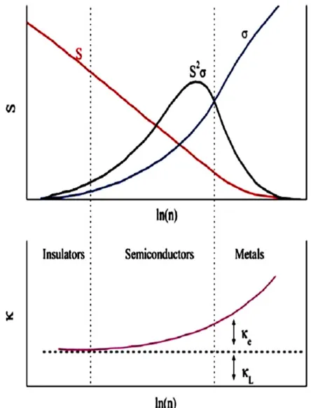
A material with high ZT needs to have a large Seebeck coefficient, existed in low carrier concentration semiconduc-tors or insulasemiconduc-tors, and a high electrical conductivity, found in high carrier concentration metals; therefore, the thermoelectric power factor maximizes somewhere between the carrier con-centrations of semiconductors and metals, as revealed inFig. 2 [32]. Specifically, the relationship between the Seebeck coeffi-cient and carrier concentration can be expressed as
S¼8p 2k2
B
3eh2 m n
T p
3n 2=3
ð5Þ
wherekBis the Boltzmann constant,eis the carrier charge,his Planck’s constant, mn
is the effective mass of the charge carrier, and n is the carrier concentration. The relationship between electrical conductivity and carrier concentration can be defined as
s¼nem ð6Þ
wheremis the carrier mobility. Typically, good thermoelectric materials are heavily doped semiconductors with carrier concentration of 1019–1021cm3
[32]. To ensure the Seebeck coefficient is large, a single type of carriers (n-type or p-type) should be remained, as mixed n-type/p-type charge carriers will lead to the opposite Seebeck effect and hence low thermopower. In order to achieve single type of carriers, it is necessary to select materials with suitable energy bandgaps and appropriate doping, in which n-type and p-type can be well separated. Therefore, effective thermoelectric materials are heavily doped semiconductors with energy bandgap less than 1 eV, in order to have both a single carrier type and sufficiently high carrier mobility. It is evident that decoupling the thermal and electronic terms that determine the ZT, including the Seebeck coefficient and electrical conductivity, has been a key strategy to improve ZT.
An effective thermoelectric material also needs to have a low thermal conductivity. Thermal conductivity of thermoelectric materials consists of two parts: kL, which results from heat
transporting phonons travelling through the crystal lattice, and ke, which arises from heat carrying charge carries (electrons or Fig. 2 Illustration of the variation of the Seebeck coefficient (S), electrical conductivity (s), power factor (S2s), electronic thermal
[image:3.595.310.532.58.349.2]holes) moving through the crystal lattice. According to the Wiedemann–Franz Law
ke¼LsT ð7Þ
where L is the Lorenz number, the electronic thermal con-ductivity is proportional to the electrical concon-ductivity, as shown inFig. 2. Therefore, to reduce the electronic component of the thermal conductivity for thermoelectric materials is not always best choice, since it will inversely affect the electrical conduc-tivity and has little or no improvement of ZT. Lattice thermal conductivity can be defined by
kl¼1=3Cuuslph ð8Þ
whereCuis heat capacity,usis the sound velocity, andlphis the
phonon mean free path (mfp). It can be seen that lattice thermal conductivity is the only parameter not determined by the electronic structure, so that enhancement of ZT can be achieved by minimizing the lattice thermal conductivity.
There are two primary methodologies in searching for thermoelectric materials with high ZT. The first approach is the ‘‘phonon glass electron crystal’’ (PGEC) approach, which suggests that an ideal thermoelectric material should be the combination of glass-like thermal conductivity and crystal-like electronic properties[39]. This approach is the most achievable in materials with complex crystal structures, where voids (vacancies) and rattlers (heavy element atoms located in the voids) would act as effective phonon scattering centres and reduce the lattice thermal conductivity significantly. The other approach is the nanostructuring of thermoelectric materials, which suggests that the ZT enhancement can be realized with nanoscale or nanostructured morphologies[33,40,41]. Nanos-tructuring can enhance the density of states (DOS) near Fermi level via quantum confinement and therefore increase the thermopower, which provides a way to decouple thermopower and electrical conductivity[33,40,41]. Besides, because mfp of electrons is much shorter than that of photons in heavily doped semiconductors, nanostructuring serves to introduce a large density of interfaces in which phonons over a large mfp range can be scattered more effectively and preferentially than electrons, as illustrated in Fig. 3, hence reducing the lattice thermal conductivity effectively while preserving carrier mobility and electronic conduction[40]. This can be satisfied
by preparation of nanostructures with one or more dimensions smaller than the mfp of phonons, while still larger than that of charge carriers.
3. Research progress on thermoelectric materials
As shown in Fig. 1a, the field of thermoelectrics advanced rapidly in the 1950s where scientific basis of thermoelectric materials became well established. The first generation of thermoelectric materials, such as Bi2Te3, PbTe and SiGe bulk
thermoelectric materials, were developed for applications at room temperature, intermediate temperature and high tem-perature, respectively. In the 1960s, the leading method for improving ZT was to control doping and form solid solutions, such as Bi2Te3–Sb2Te3, PbTe–SnTe, and Si1xGex. Although
point defects in solid solutions serve to decrease the lattice thermal conductivity by increasing heat carrying phonons scattering, there were also concurrent reductions in the charge carrier mobility, therefore, the overall ZT enhancement is limited [33]. From 1960 to 1990, the field of thermoelectrics received little attention globally, in which (Bi1xSbx)2(Se1yTey)3
alloy family remained the best commercial material with ZT of about 1 [41]. In 1990s, thermoelectric community is encouraged to re-investigate advanced thermoelectric materi-als with high performance for thermoelectric power genera-tion and cooling applicagenera-tions. For this reason, there is a revival of interest in the development of high-performance thermoelectric materials and the relevant thermoelectric theory. Over the past two decades, two different approaches have been developed to search for the next generation of thermoelectric materials: one is finding and using new families of bulk thermoelectric materials with complex crystal structures, and the other is synthesizing and using low-dimensional thermoelectric materials systems. Significant ZT improvement has been reported in the PGEC materials, and nanostructured materials, such as superlattices, quantum dots, nanowires, and nanocomposite. The key breakthroughs are highlighted inFig. 1a. Here, we will briefly mention the progress on PGEC materials and highlight the progress on nanostructured thermoelectric materials
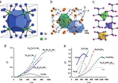
[image:4.595.182.424.533.710.2]3.1. PGEC thermoelectric materials
Slack [39] suggested that the best thermoelectric materials would behave as ‘‘phonon glass electron crystal’’, that is, it would have the thermal properties of glass-like materials and the electrical properties of crystalline materials. In typical PGEC materials, high mobility electrons are able to transport charge and heat freely, while the phonons are disrupted at the atomic scale from transporting heat. Generally, these materi-als contain a large amount of large interstitial sites filled with other element atoms, which act as ‘‘rattler’’ atoms that vibrate at low frequencies and consume thermal energy. Therefore, the PGEC materials act like a crystal for electrons while still efficiently scatter phonons, rendering these materials retaining high electrical conductivities and also obtaining low thermal conductivities. Typical examples of PGEC thermoelectric materials are skutterudites [42–52], clathrates [53–62] and
b-Zn4Sb3[22,63,64].
CoSb3 is a typical skutterudite compound, which crystal
structure is illustrated inFig. 4a. Its crystal structure belongs to body-centred cubic with eight CoSb3formula units, which
can be regarded as a simple cubic transition metal Co sublattice partially filled by almost square ring Sb4. These
rings fill six out of eight cubes formed by Co atoms, while the remaining two cubes (voids) are empty and can be filled by other atoms as ‘‘rattlers’’. The original CoSb3has a very high
power factor, but its lattice thermal conductivity is too high to be an effective thermoelectric material. One successful approach for improving ZT of these materials is proved to be void-filling in the structure with many different elements, including lanthanide, actinide, alkaline-earth, alkali, and Group IV elements [30]. These atoms can act as effective
phonon scattering centres to substantially reduce the lattice thermal conductivity. Smaller and heavier atoms in the voids would result in larger disorder and lead to larger reduction of the lattice thermal conductivity.
ZTZ1 has been achieved in filled skutterudites[42–52]. For example, Ba0.08La0.05Yb0.04Co4Sb12 has achieved a ZT of 1.7
at 850 K, which is the highest ZT value for the skutterudites as shown in Fig. 4c [52]. The clathrates are low-thermal con-ductivity compounds with open frameworks composed of tetrahedrally coordinate Si, Ge, Al, Ga, or Sn. The framework has cages that can incorporate large electropositive atoms. There are two main types of structure, so-called Type I and Type II, with the former being more common. The typical structure is shown inFig. 4b. Recent research for optimizing the thermoelectric properties of Type I clathrates above room temperature showed promising results, as shown in Fig. 4d. A Ba8Ga16Ge30crystalline ingot showed a Seebeck coefficient
of45 to150 m V K1and electrical conductivity 1500–600
Scm1
at 300–900 K [18]. The thermal conductivity of this sample decreased from 1.8 W m1K1 at 300 K to 1.25 W
m1K1at 900 K, which gave rise to ZT of 1.35[18].
3.2. Nanostructured thermoelectric materials
Low-dimensional thermoelectric materials are believed to have higher thermoelectric properties than their bulk counterparts, because the DOS near Fermi level can be enhanced via quantum confinement therefore leading to the increase of thermopower; and/or because phonons over a large mfp range can be effec-tively scattered by high density of interfaces, hence resulting in the decrease of the lattice thermal conductivity. Significant ZT
Fig. 4 (a–c) Crystal structure of CoSb3revealing the large voids with rattlers (rattlers), the type I clathrate Na8Si46, andb-Zn4Sb3,
[image:5.595.100.488.425.697.2]enhancement has been found in two-dimensional (2D) and one-dimensional (1D) thermoelectric materials.
3.2.1. 2D thermoelectric nanomaterials: quantum wells and superlattices
Kicks and Dresselhaus[65] pioneered improved ZT by two-dimensional Bi2Te3quantum well due to the enhancement of
thermopower, as quantum confinement in the interlayer direction can increase the DOS near the Fermi level. They also suggested that the interfaces between layers would effectively scatter phonons if the Bi2Te3 layer thickness was
less than phonon mfp, which would result in the decrease of lattice thermal conductivity[65,66]. As revealed inFig. 5, the ZT of Bi2Te3 quantum well structures are projected to be
much higher than its bulk counterparts. Venkatasubramanian et al.[14]observed the highest ZT¼2.4 using Bi2Te3–Sb2Te3
quantum well superlattices with a periodicity of 6 nm. Corre-spondingly, the highest ZT value for the bulk counterparts is only ZT¼1.1. Inspired by the prediction that quantum confinement may lead to an increased Seebeck coefficient and therefore higher ZT, Harman and coworkers[15] devel-oped quantum-dot superlattices in the PbTe–PbSeTe system, described as PbSe nanodots embedded in a PbTe matrix, and showed ZT¼1.6, which is significantly higher than their bulk counterparts (ZT¼0.34). Enhanced thermoelectric properties have also been found in two-dimensional thin films and quantum well structures, including Bi2Te3 superlattice-based
thin-film [67], PbTe/Ag2Te thin films [68], quantum well/
barrier PbTe/Pb1xEuxTe structures [69], and
n-PbTe/p-SnTe/n-PbTe quantum wells [70]. The early motivation for these investigations was based on the prediction that quantum confinement of in-plane carrier transport could substantially enhance the power factor over that of homogeneous materials, leading to ten-fold increases in ZT [65]. Shakouri [71]
considered that such enhancement could occur because sharp features in the electronic density of states of quantum-confined structures enable a doping-level-tuneable increase in the asymmetry between hot and cold electron transport, resulting in a large average transport energy and a large number of carriers moving in the material (i.e., a large Seebeck coefficient and electrical conductivity)[31].
Devices based on two-dimensional thermoelectric materials (such as thin film, quantum well, and superlattices) may be used for small-scale electronic and optoelectronics applica-tions where small heat loads or low levels of power generation are required [67]. However, their thermal and chemical stability associated with thermo- and electro-migration are of great concern. Especially, fully functional practical thermo-electric coolers have not been made from these nanomaterials due to the enormous difficulties in integrating nanoscale materials into microscale devices and packaged macroscale systems.
3.2.2. 1D thermoelectric nanomaterials: nanowires
Theoretical studies predict a large enhancement of ZT inside quantum wires due to additional electron confinement. Quantum nanowires were suggested to have greater enhancement in thermo-electric performance due to their stronger quantum confinement and phonon scattering, in comparison to two-dimensional coun-terparts[72]. It has also been proposed that nanotubes may have lower lattice thermal conductivity than nanowires due to their
additional phonon scattering on the inner and outer surfaces of nanotubes[73,74]. Up to date, there have been many reports on the enhancement of thermoelectric properties in one-dimensional materials. Hochbaum et al.[20]reported ZT¼0.6 can be obtained at room temperature for 50 nm diameter silicon nanowires with rough surfaces synthesized by electroless etching, which represents a 60-fold increase in ZT compared to its bulk counterpart, because the rough nanowire surface could scatter phonons effectively. The thermal conductivity, power factor and ZT of the nanowires are shown inFig. 6. Boukai et al.[19]found that thermal conductivity decreases with decreasing the nanowire diameter, and reported a ZT of 1 at 200 K for nanowires with 20 nm diameter, resulting from the significant decrease of thermal conductivity and an enhanced phonon drag contribution to the thermopower. This is the first claim that phonon drag can enhance ZT significantly in rough nanowires. Boukai et al. [19] believed that the Seebeck coefficient can be increased by the transport of certain phonon modes which have minimal contribution to thermal conductivity. It also have been reported that some nanowires have equal or lower thermoelectric properties compared to their bulk materials
[75,76], which may be due to the limited ability to control dopant and impurity concentrations in nanowires [76,77], and uninten-tional doping resulting from surface oxidation[78].
Thermoelectric measurements on individual building block, such as nanotubes, nanowires, and nanobelts, have been achieved using a suspended microheater platform [79]. How-ever, in many practical energy conversion applications, nano-wire arrays are required and the whole structure should be embedded in a matrix. A potential p–n heterostructure array used as building block to assemble thermoelectric device is proposed for potential module, as shown in the model ofFig. 7. The challenge in ensuring good electrical contact to all nanowires in the array, having high packing densities and minimizing matrix heat leakage is preventing measuring any significant enhancement in nanowire composites[31].
3.2.3. Nanocomposites
Nanostructured thermoelectric materials are designed to introduce nanometer-sized polycrystallines and interfaces into
Fig. 5 Calculated ZT as a function of layer thicknessain a quantum well structure for layers parallel to thea–bplane (1) andb–cplane (2), and the dashed line represents the optimized ZT for bulk Bi2Te3.
[image:6.595.320.542.491.689.2]bulk materials, which can reduce the lattice thermal conduc-tivity by increasing the phonon scattering. Preferential phonon scattering is possible, as the phonon mfp typically ranges from several nanometres up to a few hundred nanometres, while the carrier mfp is typically only a few nanometres[40]. Therefore, incorporation of nanostructures covering various length scales can reduce the lifetime of phonons with a broad mfp distri-bution, while charge transport can remain unchanged [40]. The approach to achieve nanostructuring composites through the formation of nanometer-sized (grain size 5 nm–10mm) polycrystallines, typically fabricated by hot pressing or spark plasma sintering of fine powders formed by grinding and milling or wet chemistry processing, in which thermoelectric
materials are prepared in nanosized particles and are then hot pressed into monoliths. Such an approach creates extensive interfaces between the neighbouring nanoparticles, which can significantly lower the thermal conductivity. The resulting nano-composites can exhibit several benefits over conventional tech-niques that create very large-grain or single crystal material, such as reduced thermal conductivity (due to phonon scattering at grain boundaries, as illustrated inFig. 3), increased power factor (due to electron filtering at grain boundaries), better mechanical properties and improved isotropy[31]. Compacting nanocrystal-line samples can be a relatively low-cost method to provide the large volume of material necessary for more wide-spread adop-tion of thermoelectric technology. ZT enhancement has been found in the many kinds of nanostructured material families, including Bi2Te3-based nanocomposites [21,80–89], PbTe-based
nanostructured materials [16,17,23,34,90–106], and SiGe-based nanocomposites[25,107].
3.2.3.1. Bi2Te3-based nanocomposites. Bi2Te3and their related
nanocomposites, the best thermoelectric materials at room temperature, are extensively used for the first thermoelectric devices for commercial Peltier elements. Bi2Te3crystals belong
to the rhombohedral crystal system with a layer structure, as shown inFig. 8. Each layer is composed of a Te–Bi–Te–Bi–Te unit, and each unit cell is composed of an ABC stacking of Te– Bi–Te–Bi–Te units along its c-axis direction. The layers are connected by the van der Waals force, while within the layer, both covalent and ionic bonds are dominated. Therefore, the
Fig. 7 p–n junction heterostructure array-based thermoelectric modulus.
[image:7.595.120.465.58.383.2] [image:7.595.65.281.429.555.2]interlayer interactions are much weaker than the intra-layer interaction.
A polycrystalline p-type Bi0.5Sb1.5Te3bulk nanocomposite (as
shown in Fig. 9), fabricated by hot pressing of ball-milled nanopowders, exhibited ZT of 1.2 at room temperature and ZT of 1.4 at 373 K[21]. The thermal conductivity was significantly reduced to 1.0 W m1
K1
in the nanocomposite from 1.3 W m1K1in the bulk ingots of the same material, although the electrical conductivity was slightly reduced in the nano-composite; therefore, the maximum ZT of the nanocomposite was almost 30% higher than the bulk ingots. Transmission electron microscopy characterization of this nanocomposite is revealed inFig. 9a–c. Complex polygonal grain structures, with diameters ranging from a few micros down to a few nanometres were detected in the nanocomposite. In addition, Sb-rich nanodots ranging from 2 to 10 nm in diameter with diffuse boundaries and pure Te precipitates with diameter between 5 and 30 nm were also observed. These nanostructures could effectively scatter phonons with a broad wavelength, which may account for the enhancement of thermoelectric properties in the nanostructrued Bi2Te3-based nanocomposites. Their following
research further show other p-type Bi2Te3-based
nanocompo-sites can also achieve a high ZT, about 1.3 between 75 and 373 K[80]and 1.4 at 373 K[81], and synthesized n-type Bi2Te3
-based nanocomposite with a ZT of 1.04 at 398 K[82]. In the reports on properties of Bi2Te3-based nanocomposites,
there exists a wide variation in ZT values, ranging from0.4 to 1.7 for nanocomposites with similar compositions. For example, a high ZT of about 1.5 at 390 K was achieved in
(Bi,Sb)2Te3nanocomposites by melt spinning single elements
of Bi, Sb, and Te followed by the spark plasma sintering process. ZT¼1.47[84]and ZT¼1.56[85,86] were achieved in nanocomposites fabricated by hot pressing of Bi2Te3 and
Sb2Te3nanopowders with diameters below 20 nm and p-type
Bi0.52Sb1.48Te3 with 5–15 nm diameter precipitates produced
by melt spinning and spark plasma sintering. Other Bi2Te3
-based nanocomposites have revealed similar thermoelectric properties to bulk Bi2Te3[73,88], while some others have poor
performance in contrast [89]. It can be deduced that the detailed structural and compositional characteristics of the nanostructures should play an important role in the thermo-electric performance.
3.2.3.2. PbTe-based nanostructured materials. A very high ZT of about 2.2 was achieved in complex nanostructured PbTe-based alloy Ag1xPb18SbTe20(LAST) fabricated by the
melt-grown method [16]. TEM analysis suggests that the LAST alloys are complex nanostructured composites contain-ing Ag–Sb-rich nanoscale inclusions, as revealed in Fig. 10, particularly when deviations from the ideal stoichiometry can be detected[16]. These nanoscale inclusions played an impor-tant role in reducing the thermal conductivity, which lead to a thermal conductivity of about 2.3 W/m K at room tempera-ture. A number of other PbTe-based nanostructured materials, including AgPbmSbTe2þm (LAST-m), AgPbmSnnSbTe2þmþn
(LASTT), NaPbmSbTe2þm(SALT-m), KPbmSbTemþ2(PLAT-m)
and PbTe-PbS, have also achieved ZT values high than 1
[17,23,90–105]. AgPbmSbTemþ2 fabricated by combining Fig. 8 Crystal structure of Bi2Te3. (a) Crystal structure of Bi2Te3with three primitive lattice vectors denoted ast1;2;3. A quintuple layer
with Te1–Bi1–Te2–Bi1–Se1is indicated by the red square; (b) Top view along thez-direction. The triangle lattice in one quintuple layer has
[image:8.595.142.467.59.359.2]mechanical alloying and spark plasma sintering methods can also achieve a high ZT of 1.5 at 700 K[106].
3.2.3.3. SiGe-based nanocomposites. A significant improve-ment in ZT was achieved in p-type SiGe nanocomposites, with a peak value about 0.95 at 1173–1223 K through a ball milling and hot-pressing method[107]. The ZT improvement
was about 90% over that of radioisotope thermoelectric generator samples (peak ZT¼0.5), and 50% over the previous highest record (0.65)[108]. A peak ZT of1.3 at 1173 K was also achieved in n-type SiGe nanocomposites using the ball milling and hot-pressing method [25], as shown in Fig. 11. Boron-doped Si/Ge nanocomposites formed by ball milling and hot pressing were also reported to significantly reduce thermal
Fig. 9 TEM images showing the microstructures of a hot-pressed BixSb2xTe3nanocomposite and their thermoelectric performance.
[image:9.595.112.476.58.424.2](a) Nanosized grains with clear grain boundaries. (b) High-magnification image showing the nanosize, high crystallinity, random orientation, and clean grain boundaries. (c) Nanodot without grain boundaries. (d) ZT. Reproduced from Ref.[21].
Fig. 10 (a) TEM image of a AgPb18SbTe20sample showing a nanosized region (a ‘‘nanodot’’ shown in the enclosed area) of the crystal
[image:9.595.120.471.479.621.2]conductivities compared to bulk SiGe alloys[41]. In addition, such SiGe nanocomposites had increased Seebeck coefficients and only slightly reduced electrical conductivities, resulting in somewhat higher power factors over the temperature range of 300–1000 K. This increased power factor for the nanocomposite is much similar to what was observed for the BixSb2xTe3 alloy and predicted
based on electron filtering effects at the grain boundaries. The materials used in thermoelectric power generation and cooling applications in the near future are nanostructured nanocomposite thermoelectric materials, as they can be assembled into a variety of desired shapes for device applications, and can be scaled up for commercial applications. These nanocomposites have already revealed dramatic improvements in thermoelectric efficiency over their bulk counterparts, and many can be fabricated through relatively inexpensive processing techniques. It should be noted that the details of the nanostructures (grain size, morphology, and compositions) and the preparation conditions must have a large impact on the performance of nanocomposite thermoelectric materials, and continued research to obtain a deeper understanding is required to allow the rational design and preparation of nanocomposites and accelerate the wide adoption of thermoelectric technologies in power generation and cooling applications.
As summarized inTable 1, reducing the size and dimension-ality of thermoelectric materials in nanoscale and nanostruc-tured materials has been demonstrated to be one of the best method to increase the thermoelectric performance, which confirmed the predicted ZT enhancement due to quantum confinement and nanostructure effects [65]. These increased ZT values result primarily from lowered thermal conduc-tivity as interface density increases, as well as from possible quantum size effects including improved thermopower result-ing from the increased electronic DOS at the Fermi level in low-dimensional systems[40]. FromTable 1, a record appar-ent highest ZT of 2.4 was reported for the Bi2Te3/Sb2Te3
superlattice system[14] and a remarkably low 300-K cross-plane value of 0.22 W m1
K1
was estimated in this Bi2Te3/
Sb2Te3 system, which is reported lowest experimental and
theoretical results in the thermoelectric system.
4. Outlook and challenge
It is of interest to note that the lowest thermal conductivity is always observed in an amorphous material, since the average
phonon mfp is on the order of the lattice constant (0.2–0.5 nm). The lowest thermal conductivity can be estimated to bek0.25– 1 W m1K1, which is confirmed by more sophisticated theories
[110]. Recent reports in superlattices of WSe2/W layers, however,
are quite intriguing as they suggested cross-plane lattice thermal conductivity values as low as 0.02 W m1
K1
[111]. While the mechanism is not fully understood, it is likely that the layering creates large asymmetry in the directional phonon density of states and low coupling between phonons in different directions. There-fore, it is believed that new physical understanding need to be urgently developed to make much lower thermal conductivity become possible.
To reach ZT values of 3 or greater, it seems to be difficult to date. It needs dramatic enhancements in the power factor, which depend on further reduction in the thermal conductivity and increase the electron conductivity. With regards to thermal conductivity, any further reduction below the amorphous limit can only occur if one can actively change the group velocity or reduce the number of phonon modes that propagate. This could result from coherent or correlated scattering effects, but so far this has remained elusive for phonons (although widely known for electrons) and thermal conductivity reduction through such mechanisms has never been conclusively demonstrated. These point to exciting scientific opportunities and create an open challenge to theorists and experimentalists alike to come up with new scattering mechanisms and concepts that will help achieve very large increases in the power factor and simultaneous decreases in thermal conductivity.
[image:10.595.122.483.59.211.2]Technically, high-performing thermoelectric properties appear to depend sensitively on the nanostructure, synthesis approach and device assembly. Various approaches will continue to study thermoelectric nanomaterials with narrow bandgaps, heavy elements doping, point defects loading and nanostructuring. Especially, for practical thermoelectric applications, the synthetic approaches of thermoelectric nanomaterials, should be: (1) scal-able, high-quality and low cost, with tuneable thermoelectric properties, (2) the nanostructured materials must be able to form dense compacts for machining/device integration (device-control-lable), (3) the nanostructured material should demonstrate an enhanced ZT over the bulk material and finally (4) the com-pacted nanoscale features should be with high thermal stability for extended periods of time. Continued research to gain a more quantitative understanding is required to allow the rational design and preparation of optimized nanostructured
Fig. 11 (a) A TEM image of a heavily doped Si80Ge20nanocomposite along with some important numerically calculated characteristic
Table 1 Thermoelectric properties of PGEC, low-dimensional and nanostructured materials synthesized by various synthetic methods in the past two decades.
Material systems Carrier type ZT kL[W m1K1] T Synthetic methodn
Ref.
Skutterudites CoSb3
Yb0.19Co4Sb12 n 1 – 600 K HP [44]
In0.25Co4Sb12 n 1.2 2 575 K SSR [45]
CoSb2.75Sn0.05Te0.20 n 1.1 2.04 823 K MAþSPS [46]
Ba0.14In0.23Co4Sb11.84 n 1.34 0.74 850 K MAGþSPS [47]
Yb0.2Co4Sb12.3 n 1.26 – 800 K MAGþSPS [48]
Yb0.3Co4Sb12.3 n 1.3 – 800 K MSþSPS [49]
Na0.48Co4Sb12 – 1.25 – 850 K MAGþHP [50]
Ba0.08La0.05Yb0.04Co4Sb12 n 1.7 – 850 K MAGþSPS [52]
2D Materials: quantum well or superlattices
PbTe/Pb1xEuxTe – 2.0 – RT MBE [69]
PbSeTe/PbTe n 2.0 0.58 RT MBE [15]
Bi2Te3/Sb2Te3 p 2.4 0.22 300 K – [14]
Bi2Te3/Bi2Te2.83Se0.17 N 1.4 0.58 300 K – [14]
Nanowire-based materials
Si nanowires – 0.6 1.2 RT EE [20]
Si nanowires p 1 – 200 K SNAP [19]
Bi2Te3-based nanocomposites
BiSbTe p 1.2 – RT HEBMþHP [21]
BiSbTe p 1.4 – 373 K HEBMþHP [21]
BiSbTe p 1.3 – 373 K HEBMþHP [80]
BiSbTe p 1.4 – 373 K HEBMþHP [81]
Bi2Te2.7Se0.3 n 1.04 – 498 K HEBMþHP [82]
(Bi,Sb)2Te3 p 1.5 – 390 K MSþSPS [83]
(BiSb)2Te3 p 1.47 – 440 K HSþHP [84]
Bi0.52Sb1.48Te3 p 1.56 0.26 300 K MSþSPS [86]
Bi2Te3 n 1 0.3 450 K HSþHP [87]
Bi0.4Sb1.6Te3 p 1.5 0.16 RT MSþHP [88]
Bi0.4Sb1.6Te3 p 1.8 – 316 K MSþHP [88]
PbTe-based nanocomposites
AgPb18SbTe20 n 2.2 – 800 K NP [16]
Ag0.5Pb6Sn2Sb0.2Te10 p 1.45 0.43 630 K NP [90]
Ag0.53Pb18Sb1.2Te20 n 1.7 – 700 K NP [91]
K0.95Pb20Sb1.2Te22 n 1.6 0.4 750 K NP [92]
Na0.95Pb20SbTe22 p 1.7 0.74 700 K NP [17]
PbTe–PbS8% n 1.4 – 750 K NP [93]
PbTe–Pb–Sb n 1.4 0.6 700 K NP [94]
PbTe–Si n 0.9 – 675 K NP [95]
Pb9.6Sb0.2Te3Se7 n 1.2 0.4 650 K NP [97]
(Pb0.95Sn0.05Te)0.92(PbS)0.08 n 1.50 0.4 642 K NP [23]
2%SrTe-containing PbTe P 1.7 0.45 800 K NP [100]
NaPb18BiTe20 p 1.3 – 670 K NP [103]
Ag0.8Pb22.5SbTe20 n 1.5 0.89 700 K MAþSPS [106]
SiGe-based nanocomposites
Si80Ge20 p 0.95 – 1073 K HEBMþHP [107]
Si80Ge20P2 n 1.3 1173 K HEBMþHP [25]
New thermoelectric materials
In4Se3d n 1.48 – 705 K Bridgeman method [26]
In4Se3xCl0.03 n 1.53 – 698 K Bridgeman method [109]
b-Cu2xSe p 1.5 0.4 1000 K MAGþSPS [28]
b-Zn4Sb3 p 1.35 – 673 K Bridgeman method [22]
n
thermoelectric materials and accelerate the wide adoption of thermoelectric technologies in power generation and cooling applications.
Acknowledgement
This work was supported by the Australian Research Council. Dr Chen thanks QLD government for a smart state future fellowship and a UQ research foundation excellent award.
References
[1] G.J. Snyder, E.S. Toberer, Complex thermoelectric materials, Nature Materials 7 (2008) 105–114.
[2] G.S. Nolas, J. Poon, M. Kanatzidis, Recent developments in bulk thermoelectric materials, MRS Bulletin 31 (2006) 199–205. [3] H. Bottner, G. Chen, R. Venkatasubramanian, Aspects of thin-film superlattice thermoelectric materials, devices, and applica-tions, MRS Bulletin 31 (2006) 211–217.
[4] T.M. Tritt, M.A. Subramanian, Thermoelectric materials, phe-nomena, and applications: a bird’s eye view, MRS Bulletin 31 (2006) 188–194.
[5] L.E. Bell, Cooling, heating, generating power, and recovering waste heat with thermoelectric systems, Science (New York, NY) 321 (2008) 1457–1461.
[6] A.J. Minnich, M.S. Dresselhaus, Z.F. Ren, G. Chen, Bulk nanostructured thermoelectric materials: current research and future prospects, Energy & Environmental Science 2 (2009) 466–479.
[7] Y.C. Lan, A.J. Minnich, G. Chen, Z.F. Ren, Enhancement of thermoelectric figure-of-merit by a bulk nanostructuring approach, Advanced Functional Materials 20 (2010) 357–376. [8] J. Baxter, Z.X. Bian, G. Chen, D. Danielson, M.S. Dresselhaus,
A.G. Fedorov, et al., Nanoscale design to enable the revolution in renewable energy, Energy & Environmental Science 2 (2009) 559–588.
[9] H.J. Goldsmid, R.W. Douglas, The use of semiconductors in thermoelectric refrigeration, British Journal of Applied Physics 5 (1954) 386–390.
[10] H.J. Goldsmid, A.R. Sheard, D.A. Wright, The performance of bismuth telluride thermojunctions, British Journal of Applied Physics 9 (1958) 365–370.
[11] J.P. Dismukes, E. Ekstrom, D.S. Beers, E.F. Steigmeier, I. Kudman, Thermalþelectrical properties of heavily doped Ge-Si alloys up to 1300 degrees K, Journal of Applied Physics 35 (1964) 2899–2907.
[12] T.C. Harman, D.L. Spears, M.J. Manfra, High thermoelectric figures of merit in PbTe quantum wells, Journal of Electronic Materials 25 (1996) 1121–1127.
[13] D.Y. Chung, T. Hogan, P. Brazis, M. Rocci-Lane, C. Kannewurf, M. Bastea, et al., CsBi4Te6: a high-performance thermoelectric material for low-temperature applications, Science (New York, NY) 287 (2000) 1024–1027.
[14] R. Venkatasubramanian, E. Siivola, T. Colpitts, B. O’Quinn, Thin-film thermoelectric devices with high room-temperature figures of merit, Nature 413 (2001) 597–602.
[15] T.C. Harman, P.J. Taylor, M.P. Walsh, B.E. LaForge, Quan-tum dot superlattice thermoelectric materials and devices, Science (New York, NY) 297 (2002) 2229–2232.
[16] K.F. Hsu, S. Loo, F. Guo, W. Chen, J.S. Dyck, C. Uher, et al., Cubic AgPbmSbTe2þm: bulk thermoelectric materials with high
figure of merit, Science (New York, NY) 303 (2004) 818–821. [17] P.F.R. Poudeu, J. D’Angelo, A.D. Downey, J.L. Short,
T.P. Hogan, M.G. Kanatzidis, High thermoelectric figure of merit and nanostructuring in bulk p-type Na1xPbmSbyTemþ2, Angewandte Chemie, International Edition 45 (2006) 3835–3839.
[18] A. Saramat, G. Svensson, A.E.C. Palmqvist, C. Stiewe, E. Mueller, D. Platzek, et al., Large thermoelectric figure of merit at high temperature in Czochralski-grown clathrate Ba8Ga16Ge30, Journal of Applied Physics 99 (2006) 023708. [19] A.I. Boukai, Y. Bunimovich, J. Tahir-Kheli, J.-K. Yu,
W.A. Goddard III, J.R. Heath, Silicon nanowires as efficient thermoelectric materials, Nature 451 (2008) 168–171.
[20] A.I. Hochbaum, R. Chen, R.D. Delgado, W. Liang, E.C. Garnett, M. Najarian, et al., Enhanced thermoelectric perfor-mance of rough silicon nanowires, Nature 451 (2008) 163–U165. [21] B. Poudel, Q. Hao, Y. Ma, Y. Lan, A. Minnich, B. Yu, et al., High-thermoelectric performance of nanostructured bismuth antimony telluride bulk alloys, Science (New York, NY) 320 (2008) 634–638.
[22] G.J. Snyder, M. Christensen, E. Nishibori, T. Caillat, B.B. Iversen, Disordered zinc in Zn4Sb3 with phonon-glass and electron-crystal thermoelectric properties, Nature Materials 3 (2004) 458–463.
[23] J. Androulakis, C.H. Lin, H.J. Kong, C. Uher, C.I. Wu, T. Hogan, et al., Spinodal decomposition and nucleation and growth as a means to bulk nanostructured thermoelectrics: enhanced performance in Pb1xSnxTePbS, Journal of the
American Chemical Society 129 (2007) 9780–9788.
[24] J.P. Heremans, V. Jovovic, E.S. Toberer, A. Saramat, K. Kurosaki, A. Charoenphakdee, et al., Enhancement of thermoelectric efficiency in PbTe by distortion of the electronic density of states, Science (New York, NY) 321 (2008) 554–557. [25] X.W. Wang, H. Lee, Y.C. Lan, G.H. Zhu, G. Joshi, D.Z. Wang, et al., Enhanced thermoelectric figure of merit in nanostructured n-type silicon germanium bulk alloy, Applied Physics Letters 93 (2008) 193121.
[26] J.S. Rhyee, K.H. Lee, S.M. Lee, E. Cho, S.I. Kim, E. Lee, et al., Peierls distortion as a route to high thermoelectric performance in In4Se3dcrystals, Nature 459 (2009) 965–968.
[27] Y. Pei, X. Shi, A. LaLonde, H. Wang, L. Chen, G.J. Snyder, Convergence of electronic bands for high performance bulk thermoelectrics, Nature 473 (2011) 66–69.
[28] H. Liu, X. Shi, F. Xu, L. Zhang, W. Zhang, L. Chen, et al., Copper ion liquid-like thermoelectrics, Nature Materials 11 (2012) 422–425. [29] T.M. Tritt, H. B ¨ottner, L. Chen, Thermoelectrics: direct solar thermal energy conversion, MRS Bulletin 33 (2008) 366–368. [30] J.R. Sootsman, D.Y. Chung, M.G. Kanatzidis, New and old
concepts in thermoelectric materials, Angewandte Chemie, International Edition 48 (2009) 8616–8639.
[31] C.J. Vineis, A. Shakouri, A. Majumdar, M.G. Kanatzidis, Nanostructured thermoelectrics: big efficiency gains from small features, Advanced Materials 22 (2010) 3970–3980.
[32] P. Vaqueiro, A.V. Powell, Recent developments in nanostruc-tured materials for high-performance thermoelectrics, Journal of Materials Chemistry 20 (2010) 9577–9584.
[33] S.K. Bux, J.P. Fleurial, R.B. Kaner, Nanostructured materials for thermoelectric applications, Chemical Communications 46 (2010) 8311–8324.
[34] M.G. Kanatzidis, Nanostructured thermoelectrics: the new paradigm?, Chemistry of Materials 22 (2009) 648–659. [35] D.L. Medlin, G.J. Snyder, Interfaces in bulk thermoelectric
materials: a review for current opinion in colloid and interface science, Current Opinion in Colloid & Interface Science 14 (2009) 226–235.
[36] P. Pichanusakorn, P. Bandaru, Nanostructured thermoelectrics, Materials Science and Engineering: R: Reports 67 (2010) 19–63. [37] M. Zebarjadi, K. Esfarjani, M.S. Dresselhaus, Z.F. Ren, G. Chen, Perspectives on thermoelectrics: from fundamentals to device applications, Energy & Environmental Science 5 (2012) 5147–5162. [38] C. Wood, Materials for thermoelectric energy-conversion,
Reports on Progress in Physics 51 (1988) 459–539.
[40] J.R. Szczech, J.M. Higgins, S. Jin, Enhancement of the thermo-electric properties in nanoscale and nanostructured materials, Journal of Materials Chemistry 21 (2011) 4037–4055.
[41] M.S. Dresselhaus, G. Chen, M.Y. Tang, R.G. Yang, H. Lee, D.Z. Wang, et al., New directions for low-dimensional thermo-electric materials, Advanced Materials 19 (2007) 1043–1053. [42] B.C. Sales, D. Mandrus, B.C. Chakoumakos, V. Keppens, J.R.
Thompson, Filled skutterudite antimonides: Electron crystals and phonon glasses, Physical Review B 56 (1997) 15081.
[43] B.C. Sales, D. Mandrus, R.K. Williams, Filled skutterudite antimonides: a new class of thermoelectric materials, Science (New York, NY) 272 (1996) 1325–1328.
[44] G.S. Nolas, M. Kaeser, R.T. Littleton, T.M. Tritt, High figure of merit in partially filled ytterbium skutterudite materials, Applied Physics Letters 77 (2000) 1855–1857.
[45] T. He, J. Chen, H.D. Rosenfeld, M.A. Subramanian, Thermo-electric properties of indium-filled skutterudites, Chemistry of Materials 18 (2006) 759–762.
[46] W.S. Liu, B.P. Zhang, L.D. Zhao, J.F. Li, Improvement of thermoelectric performance of CoSb(3x)Te(x)skutterudite com-pounds by additional substitution of IVB-group elements for Sb, Chemistry of Materials 20 (2008) 7526–7531.
[47] W. Zhao, P. Wei, Q. Zhang, C. Dong, L. Liu, X. Tang, Enhanced thermoelectric performance in barium and indium double-filled skutterudite bulk materials via orbital hybridiza-tion induced by indium filler, Journal of the American Chemical Society 131 (2009) 3713–3720.
[48] H. Li, X.F. Tang, X.L. Su, Q.J. Zhang, Preparation and thermoelectric properties of high-performance Sb additional Yb(0.2)Co(4)Sb(12þy)bulk materials with nanostructure, Applied Physics Letters 92 (2008) 202114.
[49] H. Li, X.F. Tang, Q.J. Zhang, C. Uher, Rapid preparation method of bulk nanostructured Yb(0.3)Co(4)Sb(12þy)compounds and their improved thermoelectric performance, Applied Phy-sics Letters 93 (2008) 202114.
[50] Y.Z. Pei, J. Yang, L.D. Chen, W. Zhang, J.R. Salvador, J.H. Yang, Improving thermoelectric performance of caged compounds through light-element filling, Applied Physics Letters 95 (2009) 042101.
[51] J.L. Mi, T.J. Zhu, X.B. Zhao, J. Ma, Nanostructuring and thermoelectric properties of bulk skutterudite compound CoSb3, Journal of Applied Physics 101 (2007) 054314. [52] X. Shi, J. Yang, J.R. Salvador, M. Chi, J.Y. Cho, H. Wang,
et al., Multiple-filled skutterudites: High thermoelectric figure of merit through separately optimizing electrical and thermal transports, Journal of the American Chemical Society 133 (2011) 7837–7846.
[53] X. Shi, J. Yang, S. Bai, J. Yang, H. Wang, M. Chi, et al., On the design of high-efficiency thermoelectric clathrates through a systematic cross-substitution of framework elements, Advanced Functional Materials 20 (2010) 755–763.
[54] Y. Liu, L.M. Wu, L.H. Li, S.W. Du, J.D. Corbett, L. Chen, The antimony-based type I clathrate compounds Cs(8)Cd(18) -Sb(28)and Cs(8)Zn(18)Sb(28), Angewandte Chemie, International Edition 48 (2009) 5305–5308.
[55] C.L. Condron, S.M. Kauzlarich, F. Gascoin, G.J. Snyder, Ther-moelectric properties and microstructure of Ba8Al14Si31 and EuBa7Al13Si33, Chemistry of Materials 18 (2006) 4939–4945. [56] H. Kleinke, New bulk materials for thermoelectric power
generation: clathrates and complex antimonides, Chemistry of Materials 22 (2010) 604–611.
[57] M. Christensen, B.B. Iversen, Host structure engineering in thermoelectric clathrates, Chemistry of Materials 19 (2007) 4896–4905.
[58] M. Christensen, S. Johnsen, M. Sondergaard, J. Overgaard, H. Birkedal, B.B. Iversen, Fast preparation and characterization of quarternary thermoelectric clathrates, Chemistry of Materials 21 (2009) 122–127.
[59] M. Christensen, N. Lock, J. Overgaard, B.B. Iversen, Crystal structures of thermoelectric n- and p-type Ba8Ga16Ge30studied by single crystal, multitemperature, neutron diffraction, conventional X-ray diffraction and resonant synchrotron X-ray diffraction, Journal of the American Chemical Society 128 (2006) 15657–15665. [60] M. Christensen, S. Johnsen, B.B. Iversen, Thermoelectric clathrates of type I, Dalton Transactions 39 (2010) 978–992. [61] L.T.K. Nguyen, U. Aydemir, M. Baitinger, E. Bauer, H.
Borrmann, U. Burkhardt, et al., Atomic ordering and thermo-electric properties of the n-type clathrate Ba(8)Ni(3.5)Ge(42.1) s-quare(0.4), Dalton Transactions 39 (2010) 1071–1077.
[62] U. Aydemir, C. Candolfi, H. Borrmann, M. Baitinger, A. Ormeci, W. Carrillo-Cabrera, et al., Crystal structure and transport properties of Ba(8)Ge(43)square(3), Dalton Transac-tions 39 (2010) 1078–1088.
[63] G.J. Snyder, E.S. Toberer, Complex thermoelectric materials, Nature Materials 7 (2008) 105–114.
[64] B.B. Iversen, Fulfilling thermoelectric promises: beta-Zn4Sb3 from materials research to power generation, Journal of Materials Chemistry 20 (2010) 10778–10787.
[65] L.D. Hicks, M.S. Dresselhaus, Effect of quantum-well structures on the thermoelectric figure of merit, Physical Review B 47 (1993) 12727.
[66] L.D. Hicks, T.C. Harman, M.S. Dresselhaus, Use of quantum-well superlattices to obtain a high figure of merit from nonconventional thermoelectric materials, Applied Physics Let-ters 63 (1993) 3230–3232.
[67] I. Chowdhury, R. Prasher, K. Lofgreen, G. Chrysler, S. Narasimhan, R. Mahajan, et al., On-chip cooling by superlattice-based thin-film thermoelectrics, Nature Nanotech-nology 4 (2009) 235–238.
[68] J.J. Urban, D.V. Talapin, E.V. Shevchenko, C.R. Kagan, C.B. Murray, Synergism in binary nanocrystal superlattices leads to enhanced p-type conductivity in self-assembled PbTe/ Ag2Te thin films, Nature Materials 6 (2007) 115–121. [69] L.D. Hicks, T.C. Harman, X. Sun, M.S. Dresselhaus, Experimental
study of the effect of quantum-well structures on the thermoelectric figure of merit, Physical Review B 53 (1996) R10493.
[70] E.I. Rogacheva, O.N. Nashchekina, A.V. Meriuts, S.G. Lyub-chenko, M.S. Dresselhaus, G. Dresselhaus, Quantum size effects in n-PbTe/p-SnTe/n-PbTe heterostructures, Applied Physics Letters 86 (2005) 063103.
[71] A. Shakouri, Thermoelectric, thermionic and thermophotovoltaic energy conversion, Proceedings of the International Conference on Thermoelectrics (2005) 492–497.
[72] L.D. Hicks, M.S. Dresselhaus, Thermoelectric figure of merit of a one-dimensional conductor, Physical Review B 47 (1993) 16631–16634.
[73] X.B. Zhao, X.H. Ji, Y.H. Zhang, T.J. Zhu, J.P. Tu, X.B. Zhang, Bismuth telluride nanotubes and the effects on the thermoelectric properties of nanotube-containing nanocomposites, Applied Physics Letters 86 (2005) 062111.
[74] G. Zhang, Q. Yu, W. Wang, X. Li, Nanostructures for thermo-electric applications: synthesis, growth mechanism, and property studies, Advanced Materials 22 (2010) 1959–1962.
[75] A.I. Persson, Y.K. Koh, D.G. Cahill, L. Samuelson, H. Linke, Thermal conductance of InAs nanowire composites, Nano Letters 9 (2009) 4484–4488.
[76] A. Mavrokefalos, A.L. Moore, M.T. Pettes, L. Shi, W. Wang, X. Li, Thermoelectric and structural characterizations of individual electrodeposited bismuth telluride nanowires, Journal of Applied Physics 105 (2009) 104318.
[77] F. Zhou, J.H. Seol, A.L. Moore, L. Shi, Q.L. Ye, R. Scheffler, One-dimensional electron transport and thermopower in an individual InSb nanowire, Journal of Physics: Condensed Matter 18 (2006) 9651–9657.
of indium antimonide nanowires, Journal of Physics D: Applied Physics 43 (2010) 025406.
[79] P. Kim, L. Shi, A. Majumdar, P.L. McEuen, Mesoscopic thermal transport and energy dissipation in carbon nanotubes, Physica B: Condensed Matter 323 (2002) 67–70.
[80] Y. Ma, Q. Hao, B. Poudel, Y. Lan, B. Yu, D. Wang, et al., Enhanced thermoelectric figure-of-merit in p-type nanostruc-tured bismuth antimony tellurium alloys made from elemental chunks, Nano Letters 8 (2008) 2580–2584.
[81] Y. Lan, B. Poudel, Y. Ma, D. Wang, M.S. Dresselhaus, G. Chen, et al., Structure study of bulk nanograined thermo-electric bismuth antimony telluride, Nano Letters 9 (2009) 1419–1422.
[82] X. Yan, B. Poudel, Y. Ma, W.S. Liu, G. Joshi, H. Wang, et al., Experimental studies on anisotropic thermoelectric properties and structures of n-Type Bi(2)Te(2.7)Se(0.3), Nano Letters 10 (2010) 3373– 3378.
[83] W. Xie, J. He, H.J. Kang, X. Tang, S. Zhu, M. Laver, et al., Identifying the specific nanostructures responsible for the high thermoelectric performance of (Bi,Sb)2Te3 nanocomposites, Nano Letters 10 (2010) 3283–3289.
[84] Y.Q. Cao, X.B. Zhao, T.J. Zhu, X.B. Zhang, J.P. Tu, Syntheses and thermoelectric properties of Bi(2)Te(3)/Sb(2)Te(3)bulk nano-composites with laminated nanostructure, Applied Physics Letters 92 (2008) 143106.
[85] W. Xie, X. Tang, Y. Yan, Q. Zhang, T.M. Tritt, High thermo-electric performance BiSbTe alloy with unique low-dimensional structure, Journal of Applied Physics 105 (2009) 113713. [86] W. Xie, X. Tang, Y. Yan, Q. Zhang, T.M. Tritt, Unique
nanostructures and enhanced thermoelectric performance of melt-spun BiSbTe alloys, Applied Physics Letters 94 (2009) 102111.
[87] X.B. Zhao, S.H. Yang, Y.Q. Cao, J.L. Mi, Q. Zhang, T.J. Zhu, Synthesis of nanocomposites with improved thermoelectric properties, Journal of Electronic Materials 38 (2009) 1017–1024. [88] S. Fan, J. Zhao, J. Guo, Q. Yan, J. Ma, H.H. Hng, p-type Bi(0.4)Sb(1.6)Te(3)nanocomposites with enhanced figure of merit, Applied Physics Letters 96 (2010) 182104.
[89] X.A. Fan, J.Y. Yang, Z. Xie, K. Li, W. Zhu, X.K. Duan, et al., Bi2Te3hexagonal nanoplates and thermoelectric properties of n-type Bi2Te3 nanocomposites, Journal of Physics D: Applied Physics 40 (2007) 5975–5979.
[90] J. Androulakis, K.F. Hsu, R. Pcionek, H. Kong, C. Uher, J.J. Dangelo, et al., Nanostructuring and high thermoelectric efficiency in p-type Ag(Pb1ySny)(m)SbTe2þm, Advanced
Mate-rials 18 (2006) 1170–1173.
[91] B.A. Cook, M.J. Kramer, J.L. Harringa, M.K. Han, D.Y. Chung, M.G. Kanatzidis, Analysis of nanostructuring in high figure-of-merit Ag(1x)Pb(m)SbTe(2þm)thermoelectric mate-rials, Advanced Functional Materials 19 (2009) 1254–1259. [92] P.F.P. Poudeu, A. Gueguen, C.-I. Wu, T. Hogan,
M.G. Kanatzidis, High figure of merit in nanostructured n-type KPb(m)SbTe(mþ2)thermoelectric materials, Chemistry of Materials 22 (2010) 1046–1053.
[93] S.N. Girard, J. He, C. Li, S. Moses, G. Wang, C. Uher, et al., In situ nanostructure generation and evolution within a bulk thermoelectric material to reduce lattice thermal conductivity, Nano Letters 10 (2010) 2825–2831.
[94] J.R. Sootsman, H. Kong, C. Uher, J.J. D’Angelo, C.-I. Wu, T.P. Hogan, et al., Large enhancements in the thermoelectric power factor of bulk PbTe at high temperature by synergistic nanostructuring, Angewandte Chemie, International Edition 47 (2008) 8618–8622.
[95] J.R. Sootsman, J. He, V.P. Dravid, S. Ballikaya, D. Vermeulen, C. Uher, et al., Microstructure and thermoelectric properties of
mechanically tobust PbTe–Si eutectic composites, Chemistry of Materials 22 (2010) 869–875.
[96] J. He, S.N. Girard, M.G. Kanatzidis, V.P. Dravid, Micro-structure-lattice thermal conductivity correlation in nano-structured PbTe(0.7)S(0.3) thermoelectric materials, Advanced Functional Materials 20 (2010) 764–772.
[97] P.F.P. Poudeu, J. D’Angelo, H. Kong, A. Downey, J.L. Short, R. Pcionek, et al., Nanostructures versus solid solutions: low lattice thermal conductivity and enhanced thermoelectric figure of merit in Pb9.6Sb0.2Te10xSexbulk materials, Journal of the
American Chemical Society 128 (2006) 14347–14355.
[98] E. Quarez, K.F. Hsu, R. Pcionek, N. Frangis, E.K. Polychro-niadis, M.G. Kanatzidis, Nanostructuring, compositional fluc-tuations, and atomic ordering in the thermoelectric materials AgPbmSbTe2þm. The myth of solid solutions, Journal of the
American Chemical Society 127 (2005) 9177–9190.
[99] J. He, J.R. Sootsman, S.N. Girard, J.C. Zheng, J. Wen, Y. Zhu, et al., On the origin of increased phonon scattering in nanos-tructured PbTe based thermoelectric materials, Journal of the American Chemical Society 132 (2010) 8669–8675.
[100] K. Biswas, J. He, Q. Zhang, G. Wang, C. Uher, V.P. Dravid, et al., Strained endotaxial nanostructures with high thermo-electric figure of merit, Nature Chemistry 3 (2011) 160–166. [101] J.R. Sootsman, R.J. Pcionek, H. Kong, C. Uher, M.G.
Kanat-zidis, Strong reduction of thermal conductivity in nanostruc-tured PbTe prepared by matrix encapsulation, Chemistry of Materials 18 (2006) 4993–4995.
[102] M.-K. Han, K. Hoang, H. Kong, R. Pcionek, C. Uher, K.M. Paraskevopoulos, et al., Substitution of Bi for Sb and its role in the thermoelectric properties and nanostructuring in Ag1xPb18MTe20 (M¼Bi, Sb) (x¼0, 0.14, 0.3), Chemistry of Materials 20 (2008) 3512–3520.
[103] Al Gueguen, P.F.P. Poudeu, C.-P. Li, S. Moses, C. Uher, J. He, et al., Thermoelectric properties and nanostructuring in the p-type materials NaPb18xSnxMTe20(M¼Sb, Bi), Chemis-try of Materials 21 (2009) 1683–1694.
[104] K. Ahn, C.-P. Li, C. Uher, M.G. Kanatzidis, Thermoelectric properties of the compounds AgPbmLaTemþ2, Chemistry of Materials 22 (2009) 876–882.
[105] C.B. Lioutas, N. Frangis, I. Todorov, D.Y. Chung, M.G. Kanatzidis, Understanding nanostructures in thermoelectric materials: an electron microscopy study of AgPb18SbSe20 crys-tals, Chemistry of Materials 22 (2010) 5630–5635.
[106] M. Zhou, J. Li, T. Kita, Nanostructured AgPbmSbTemþ2system
bulk materials with enhanced thermoelectric performance, Journal of the American Chemical Society 130 (2008) 4527–4532. [107] G. Joshi, H. Lee, Y. Lan, X. Wang, G. Zhu, D. Wang
et al., Enhanced thermoelectric figure-of-merit in nanostructured p-type silicon germanium bulk alloys, Nano Letters 8 (2008) 4670– 4674.
[108] C.B. Vining, W. Laskow, J.O. Hanson, R.R. Vanderbeck, P.D. Gorsuch, Thermoelectric properties of pressure-sintered Si0.8Ge0.2thermoelectric alloys, Journal of Applied Physics 69 (1991) 4333–4340.
[109] J.S. Rhyee, K. Ahn, K.H. Lee, H.S. Ji, J.-H. Shim, Enhancement of the thermoelectric figure-of-merit in a wide temperature range in In4Se3xCl0.03 bulk crystals, Advanced Materials 23 (2011) 2191–2194.
[110] D.G. Cahill, S.K. Watson, R.O. Pohl, Lower limit to the thermal-conductivity of disordered crystals, Physical Review B 46 (1992) 6131–6140.
Professor Jin Zou received his Ph.D. in Materials Physics from the University of Sydney and worked there for 10 years as a researcher. He is now a Chair in Nanoscience at the University of Queensland. His research interests focus on the nanocharacterization of various semiconductor and functional nanos-tructures; and he published about 400 journal publications in this field.


![Fig. 11(a) A TEM image of a heavily doped Si80Ge20 nanocomposite along with some important numerically calculated characteristiclengths [6], and (b) typcial ZT](https://thumb-us.123doks.com/thumbv2/123dok_us/164558.41702/10.595.122.483.59.211/image-heavily-nanocomposite-important-numerically-calculated-characteristiclengths-typcial.webp)

