Bachelor of Science
CALIFORNIA INSTITUTE OF TECHNOLOGY Pasadena, California
2018
© 2018 Rita Frances Sonka ORCID: 0000-0002-1187-9781
Cosmic Microwave Background that has led my scientific pursuits ever since. Thank you for the many weekly meetings, patient guidance, and general introduction to the world of academia.
I would like to thank the Caltech SURF office and the Caltech Senior thesis program as well for providing me such an incredible opportunity to pursue my research interests as an undergraduate.
I would like to thank several Bock lab members who encouraged me, lent me figures, and/or helped teach me the details of experimental work in physics and general and the Bock Lab in particular. Thank you to Cheng Zhang, Ahmed Mohamed, Howard Hui, Jonathen Hunacek, and Sinan Kefeli.
ABSTRACT
The successful detection and characterization of the B-modes in the Cosmic Mi-crowave Background (CMB) would dramatically illuminate the physics of the infla-tionary era. The Observational Cosmology Group is iterating on bolometers in an attempt to detect this signal. The previous detector design became unstable in parts of its transition when adjusted for 220/270 GHz frequencies, limiting its use.
We study the mechanism of instability in these transition edge sensor (TES) bolome-ters used for ground based observations of the Cosmic Microwave Background (CMB) at 270GHz. The instability limits the range of useful operating resistances of the TES down to≈ 50% of Rn, and due to variations in detector properties and optical loading within a column of multiplexed detectors, limits the effective on sky yield to≈67 %.
Through comparison of 7 new detector thermal capacity designs and measurements of the electrical impedance of the detectors, we show the instability is due to the increased bolometer legGfor higher-frequency detection inducing decoupling of the palladium-gold heat capacity from the thermistor. We demonstrate experimentally that the limiting thermal resistance is due to the small cross sectional area of the silicon nitride bolometer island, and so is easily fixed by layering palladium-gold over an oxide protected TES. The resulting detectors can be biased down to a resistance≈10% of Rn, improving the effective on-sky yield to≈93 %.
2.1 Transition Edge Sensor Bolometers . . . 2
2.2 The IV and PR curve of the Ideal TES . . . 3
2.3 Thermal instability issue . . . 6
2.4 Bolometer decoupling model . . . 8
2.5 Modification Logic and Designs . . . 10
2.6 The Aluminum PR curve investigation . . . 12
Chapter III: Methods: Data Acquisition . . . 15
3.1 IV curves data acquisition . . . 15
3.2 Superfast data acquisition . . . 19
3.3 Bolometer impedance acquisition . . . 19
Chapter IV: Methods: Analysis . . . 21
4.1 Titanium TES . . . 21
4.2 Aluminum TES . . . 23
4.3 Superfast . . . 24
4.4 Impedance . . . 24
Chapter V: Results . . . 26
5.1 Titanium IV curves . . . 26
5.2 Aluminum PR Slope Models and Fit Results . . . 27
5.3 Superfast preliminary results . . . 31
5.4 Impedance . . . 32
Chapter VI: Conclusions . . . 35
Bibliography . . . 36
Appendix A: Titanium sample IV, PR and transition-select plots for all types . 38 A.1 Characteristic IV plots . . . 38
A.2 PR transition-select plots . . . 41
LIST OF ILLUSTRATIONS
Number Page
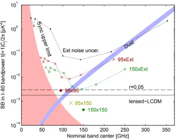
1.1 This plot of "signal strength/CMB signal strength" as a function of frequency shows the latest noise constraints on the B-mode signal, accompanied by the latest bounds on the signal’s magnitude. The red patch shows allowed false-signal magnitudes of synchrotron radia-tion. The purple band shows allowed false-signal magnitudes from dust. The horizontal black lines are upperbounds on the B-mode signal’s magnitude. Note how they have lowered enough that there is essentially no avoiding both the dust and synchrotron radiation errors, and one must be subtracted out regardless of what frequency the signal is pursued at. As the dust model is better constrained, it was chosen to use for subtraction. The 220/270 GHz range has neg-ligible synchrotron radiation noise while still being somewhat close to the primary data taking range around 150 GHz, and thus is ideal for imaging the dust. Image Credit [4] . . . 1 2.1 Basics of bolometers. Image credit: D.F. Santavicca, licensed under
Creative Commons Attribution 3.0 . . . 2 2.2 Superconductor Temperature vs. Resistance. . . 2 2.3 The ideal IV and PR curves, as illustrated by one of our detectors
after the instability issue was fixed. . . 3 2.4 Ideal TES thermal and electrical circuit. In the ideal case, the island
2.6 Original (type A) detector characteristic IV and PR plots. . . 6
2.7 Fully functional (type F) detector IV and PR plot. . . 7
2.8 Bolometer thermal (black) and electrical (green) circuit. . . 8
2.9 Original SF data that helped prompt this thesis. . . 8
2.10 Above: Annotated photograph under microscope of a control group (A-type) detector. Below: Diagram of side view along blue line on the photograph, not to scale. In green: location of the relevant 150 µm2 island cross section. Note the green dimensions line on the photograph had to be moved to the side; the side view green dimension line shows the relevant location along the island’s length. 9 2.11 Photographs of the 8 bolometer designs. . . 12
2.12 The cuts of the aluminum transitions for the type D (above) and type F (below) detectors. Red lines mark the start and ends of the selected transition region from the data (blue). Note the differences in how the transitions end. . . 12
2.13 The early cutoff in the plot is due to a limitation of the equipment’s ability to put large currents through the device. However, the large slope in the transition region was unexpected. . . 13 3.1 FPU # 1 temperature during the successful data-taking run is in pink.
Note that the temperature of the detectors exceeds the FPU # 1 plane during the application of the critical current (“zapping”) that occurred at the top of each peak, and for some time thereafter as data was taken. 16 3.2 An example of raw data for some of the IV curves at 254mK. Displays
3.3 Simplified version of the TES circuit. The inductor is used to read out the circuit by projecting a magnetic field; ideally, there is only a negligible voltage drop across it when data is being read. . . 18 3.4 Type G "double transition" Rn failure IV plot. . . 19 4.1 Ideal superconductor resistance curve. Note that as per the heat
equa-tion, the power dissipated in the detectors is related to the temperature of the detectors; the more power dissipated, the higher a temperature difference will be established between the detectors and bath. . . 21 4.2 A particularly bad column (mce column 3) of Algorithm 1 (local
standard deviation change) PR plot results for the 254 mK run. Con-sider, for example, the row 9 detector. Blank plots has failed or absent detectors, or failed SQUIDS. . . 22 4.3 The same column algorithm 1 failed on, much improved in the final
algorithm. . . 22 4.4 These residuals are small compared to the actual values. . . 24 5.1 Type A transition range graph at a bath temperature of 254mK. The
x axes are the current applied to the TES shunt resistors. The vertical line shows the optimal current where the largest number of detectors are operating simultaneously. In the left plot, horizontal bars show the limits of the in transition for each detector of type A. The right plot shows the count of in transition detectors for each bias current. . 27 5.2 Type F transition range graph at a bath temperature of 254mK.
Com-pared to Fig. A.17, the stable bias regions are much wider for each detector. . . 27 5.3 Mean length in which a detector was usable (in RT E S/Rn %) vs.
Temperature (in mK). Higher is better. Types A, B, C and H increase in stability with temperature while the others do not, consistent with decreasing loopgain allowing them to satisfy the thermal stability criterion that D,E,F,G have already met. . . 27 5.4 A reminder of the issue seen in the Aluminum that we can plausibly
investigate. The early cutoff in the plot is due to a limitation of the equipment’s ability to put large currents through the device. However, the large slope in the transition region was unexpected. . . 28 5.5 The two main models attempted, with fits given for a sample A-type
5.9 Fourier analysis of A-type detector for various current biases in DAC; amplitude vs. frequency. Note the "bump" of increase in frequency
amplitude a bit bast 104. . . 31
5.10 Fourier analysis of F-type detector for various current biases in DAC; amplitude vs. frequency. Note the lack of a "bump" of increase in frequency amplitude a bit bast 104. . . 31
5.11 Fourier analysis of D-type detector for various current biases in DAC; amplitude vs. frequency. Note the lack of a "bump" of increase in frequency amplitude a bit bast 104. . . 32
5.12 Fitted admittance for representative type A (top) and F (bottom) bolometers. Points are measured data, one point per frequency, lines are fits to the model. Color shows the bias voltage. Data is shown down to the lowest bias voltage where the detector remained stable. . 33
5.13 Histogram of fitted γfor the A,B,E and F detectors. . . 34
A.1 Type A characteristic IV plot. . . 38
A.2 Type B characteristic IV plot. . . 39
A.3 Type C characteristic IV plot. . . 39
A.4 Type D characteristic IV plot. . . 39
A.5 Type E characteristic IV plot. . . 40
A.6 Type F characteristic IV plot. . . 40
A.7 Type G functional characteristic IV plot. . . 40
A.8 Type H functional characteristic IV plot. . . 41
A.9 Type A PR transition-select graph at 254mK. . . 41
A.10 Type B PR transition-select graph at 254mK. . . 42
A.11 Type C PR transition-select graph at 254mK. . . 42
A.13 Type E PR transition-select graph at 254mK. . . 43
A.14 Type F PR transition-select graph at 254mK. . . 44
A.15 Type G PR transition-select graph at 254mK. . . 44
A.16 Type H PR transition-select graph at 254mK. . . 45
A.17 Type A transition range graph at 254mK. . . 46
A.18 Type B transition range graph at 254mK. . . 47
A.19 Type C transition range graph at 254mK. . . 48
A.20 Type D transition range graph at 254mK. . . 49
A.21 Type E transition range graph at 254mK. . . 50
A.22 Type F transition range graph at 254mK. . . 51
A.23 Type G transition range graph at 254mK. . . 52
C h a p t e r 1
MOTIVATION AND INTRODUCTION
The Bock Observational Cosmology Group at Caltech is attempting to find a par-ticular signature in the Cosmic Microwave Background (CMB): the B-Modes that are created by gravitational waves [5]. A successful detection and characterization of these B-Modes would provide an enormous amount of information about the physics of the inflationary era, the brief period in which the universe expanded superluminally [10].
C h a p t e r 2
BACKGROUND, ISSUE AND THEORY
2.1 Transition Edge Sensor Bolometers
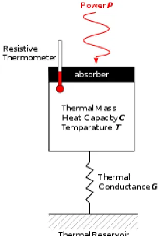
Basic bolometers are devices that measure incident radiation (see Fig. 2.1). The radiation heats an absorber; because the material is only weakly connected to the bath (thermal reservoir), this raises the temperature of the absorber (and thus the amount of power flowing through the thermal link) until thermal equilibrium is reached with the bath. The temperature of the absorber is measured to determine how much power is being deposited on the bolometer.
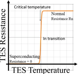
[image:14.612.114.272.440.671.2]A Transition Edge Sensor (TES) bolometer is a device that measures power of incident electromagnetic radiation by heating (via bias wires) a superconductor to keep it at its critical temperature (see Fig. 2.2), where it has extremely temperature-dependent electrical resistance [17]. The amount of electrical power needed to have it maximally vary in resistance is what is measured during normal operation; less power is required if the bolometer receives more optical power.
Figure 2.2: Superconductor Temperature vs. Resistance.
2.2 The IV and PR curve of the Ideal TES
We explain and derive the Ideal TES IV and PR curves, as illustrated in Fig. 2.3. Begin with the outside-transition regions.
As indicated in figure 2.2, the TES has zero resistance while superconducting. This causes all of the current to flow dissipationlessly through the superconductor (and none of it through the shunt resistor), with IT E S = Ibias. While our measurement system does capture this proportionality (while not clearly visible due to the dif-ferently scaled axes, the slope of the line in this region is 1), the sudden jump in current as the TES latches superconducting messes up the calibration that holds in all above-superconducting currents, causing it to be off by a constant (hence why it doesn’t go through 0). This off-by-constant data (and the fact that the TES actually has 0 resistance) means this portion of the PR curve is meaningless, except to show that the transition has ended.
As indicated in figure 2.2, the TES has constant, normal resistance above a certain temperature. It thus obeys Ohm’s law for the IV and PR curves in these regions.
Figure 2.3: The ideal IV and PR curves, as illustrated by one of our detectors after the instability issue was fixed.
characteristic in-transition IV curve for our TES, assuming it was ideal.
Start with the thermal circuit depicted in black in Fig. 2.4. The thermal differential equation is, by the definition of heat capacity:
CdTT E S
dt =−Pt h +Popt +Pel (2.1)
The appropriate thermal conductance equation forPt h is [11]:
Pt h = K(TT E Sn −Tbat hn ) (2.2)
where K = G/(nTT E Sn−1), G = the dynamic thermal conductance = dTdPT E Sth and n = β + 1, β the thermal conductance exponent [15]. Our TES n is 3.5 ([1] gives β but calls it n). Importantly, dTdKT E S = 0; this can be seen by taking the derivative of Eq. 2.2. Consequently, for small signals nearT c = Titanium critical temperature, we can take the first order Taylor expansion and obtain
Pt h ≈ Pt hC +G(TT E S−Tbat h) (2.3)
Figure 2.4: Ideal TES thermal and electrical circuit. In the ideal case, the island and the TES are much better connected than the link through the island’s legs to the bath, and thus they are at the same temperature, and the island’s is the only relevant heat capacity because it dwarfs the TES’s.
Now consider the ideal electrical circuit, depicted in green in 2.4. For our IV curves, we run DC current, so the inductor is negligible; in the ideal case the inductor also has 0 resistance. Then V on each branch of the green electrical circuit is
V = Ibias∗ ( 1
1
Rshunt +
1
RT E S
) (2.4)
For our detectors, RT E S >> Rshunt in the transition range, so V is effectively independent ofRT E S, and close to proportional toIbias. This is the "V" in the phrase "IV curves," which looks at the current through the TES as a function of the voltage applied to it, at a given temperature. So sincePel=V2/RT E S, we have that:
Pel =V2/RT E S =
I b2R2
shuntRT E S
(Rshunt+ RT E S)2
(2.5)
Eq. 2.5 captures the most critical facet of a functional TES, electrothermal feedback. As the power delivered to RT E S (either electrically or optically) increases, TT E S
increases, so RT E S increases (as per Fig. 2.2), bringing down the power dissipated in it and returning the temperature toTC. As the power delivered to RT E S (either electrically or optically) decreases,TT E S decreases, so RT E S decreases (as per Fig. 2.2), bringing down the power dissipated in it and returning the temperature toTC
depending on how much power the TES is receiving from the varying optical or bias power.).
Now, since in equilibrium (and our device has time to reach equilibrium during each point in the IV curves)Pt h = Popt+Pel, and as we just explained the device stays at aboutTCwhile in the transition region, and since our IV curves are a dark run with non optical power, and with reference to Eq. 2.3:
Pt hC+G(TT E S−TC)= Pt hC = Popt +Pel = Pel (2.6)
Which we can solve to obtain
RT E S(Ibias)@(TT E S =TC)=
−2Pt hCRshunt+Ibias2 R2shunt−
q −4I2
biasPt hCRshunt3 +Ibias4 Rshunt4
2Pt hC
(2.7)
ThenIT E S =V/RT E S. IT E S evaluates as given at the top of Fig. 2.5.
The ideal PR curve is a flat line in the transition region, as can be seen by plugging in the appropriate values for P and R.
On-sky measurement thus compares the amount of power that must be supplied via bias to keep the TES at its critical temperature to the measured Pt hC = PSatur ation
for the given focal plane (bath) temperature with no optical power. The less power that needs to be supplied, the more optical power the detector is recording.
Two other particularly important qualities for our TES’s areαand theL.
The resistive transition sharpness parameterαmeasures steepness of the transition at the critical temperature (reference Fig. 2.2):
α= d(log(R))
d(log(T)) (2.8)
L is the DC (current) loopgain:
− δPel
δPopt
=L = αPel
GT (2.9)
2.3 Thermal instability issue
This thesis was prompted by the fact that the original 220/270 GHz detector design did not sufficiently conform to the ideal.
The bolometer thermal conductivityGused for 270GHz imaging in a ground based experiment must be higher than that used for 95,150 or 220GHz due to the increased atmosphere temperature; more power is incident on the detectors, so more must be vented to keep them at critical temperature. In the detectors designed for the Keck experiment at 270GHz, we found that the stable operating region for these higher
G detectors was limited, and the detectors would latch if operated at fractional
resistances less than≈50% of the normal resistance, as shown in Fig. 2.6; compare Fig. 2.7.
While individually our detectors have high yield, when they are multiplexed into a large format array using a time multiplexing system (in which each detector is read out one at a time in sequence), the yield is limited by the requirement that a column of 32 detectors is DC biased with a single bias voltage. Variations in detector properties and optical loading across the focal plane cause variations in the optimal bias point for the detectors. In the lower frequency instruments, the stable regions were wide enough that the constant voltage within a column requirement did not impact yield. In contrast, the limited stability of the 270GHz detectors precluded operation of all the detectors in a column at a single bias. In the dark measurements presented here, even with no optical power variations, the simultaneously biased into transition yield was at best 67% for the baseline detector design, as shown in Fig. A.17.
In an ideal bolometer, the bolometer is connected directly to a cold bath that it
0 2 4 6 8
Ibias [Amps] 10-4
-8 -6 -4 -2 0 2 4 6 8 10 12 Ites [Amps] 10-5
Rn: 73.76 m
0 50 100 150 200
TES R [m ] 0 2 4 6 8 10 12 14 16 18 20
TES P [pW]
254 259 273 297 320 334 350 368 380 404 429 443 480
Figure 2.8: Bolometer thermal (black) and electrical (green) circuit.
vents its heat out of as per the heat equation [8]. In practice, there is more than one material the heat must flow through to reach a bath with sufficient heat capacity. This is irrelevant if these connections have sufficiently different thermal conductivities that the system is effectively modeled by only considering the lowest. However, the 220/270 GHz needed to have higher island-bath leg conductivities in order to vent the greater heat from the higher frequency light. Upon observing the instability issue, and inspired by the work of George et al [6], it was theorized this increase was enough to effectively split the bolometer thermal circuit into a two-stage system, as illustrated in Fig. 2.8; thus that the stability of the detectors was limited by the TES-heat capacity coupling, rather than limited electrical bandwidth[11].
Figure 2.9: Original SF data that helped prompt this thesis.
capacity to G be greater than the electrothermal feedback loopgain. Increasing the detector G for higher frequency detectors without changing the island design decreasedγto a point where it fell below the loopgain achievable from the steepness of the superconducting transition. The thermal circuit of this model is depicted in Fig. 2.8, and leads to the following stability criterion:
L < γ +1+ CT E S
Gγγ+
1τe
≈ γ. (2.10)
CT E S is the heat capacity of the titanium TES andτeis the electrical time constant
of the readout circuit L/R. The term GCT E Sγ γ+1τe
is negligible becauseCT E S <<Ci, so
CT E S
G <<
Ci
G = τ0 < τe, whereCiis the heat capacity of the bolometer island.
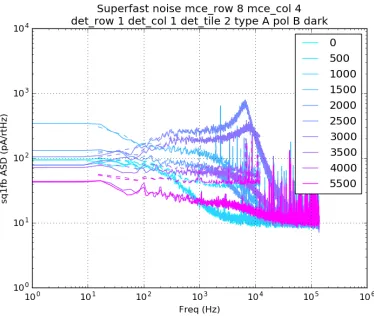
Part of what made us suspect that the two-stage system thermal instability was the cause of our odd IV curves was a superfast analysis on the original, flawed detectors, that revealed a surprising upwards peak at a bit past the Rshunt/L value (L for us is 1.35 µH), as depicted in Fig. 2.9. This seemed to indicate the circuit losing electrothermal feedback and oscillating unstably.
2.4 Bolometer decoupling model
Figure 2.10: Above: Annotated photograph under microscope of a control group (A-type) detector. Below: Diagram of side view along blue line on the photograph, not to scale. In green: location of the relevant 150 µm2island cross section. Note the green dimensions line on the photograph had to be moved to the side; the side view green dimension line shows the relevant location along the island’s length.
The thermal conductance of a rectangular aperture of an insulator reaches a limiting value as the insulator gets thinner, determined by the Stefan-Boltzmann law for radiation. The limiting value in silicon nitride has been shown to be consistent with this model[9][20]:
G =4ΣAT3 (2.11)
and the PdAu heat capacity must pass through this small aperture for the baseline A type detector (see green text in Fig. 2.10 for relevant cross section location.). For the titanium transition critical temperature Tc = 0.5K, this is a decoupling thermal conductance of Gint = 12nW/K. For a typical leg thermal conductivity
G ≈ 150pW/K, γ ≈ 80, and stable detector operation will be limited to loop gain L < 80.
The heat capacity of the titanium TES we estimate atCT E S = 0.016pJ/K from its volume, 100µm3, the critical temperature of our titanium filmsTc = 0.50K, and the bulk electronic heat capacity of titanium, 310 Jm−3K−2. The island heat capacity we estimateCi = 4.8pJ/K, from the measured bolometerτ0andG. BecauseCT E S
is so small compared to theCi, we neglect including it in the model for the bolometer impedance.
A second possibility for the thermal resistance is the electron-phonon coupling, i.e. hot electron effects. Measurements of the electron phonon relaxation time in titanium films[7][19] give 1-3 microseconds at 0.5K, though in films withTc < 0.5K. Given a TES volume of≈100µm3,Ge−ph =6−17nW/K, orγ = 40−110. Ge−ph
and Gint are quite similar but we can distinguish between them by modifying the bolometer to bring the palladium-gold closer to the TES with or with out direct electrical contact.
2.5 Modification Logic and Designs
As per Eq. 2.10, in order to stabilize, we must either increaseγ(decrease the internal thermal resistance of the island) or decrease the loopgainL. We prefer the former, as high loopgain enables faster measurements, but will also investigate the latter.
IfGint is the main bottleneck, we can increase γ by layering PdAu over either the Titanium or the Aluminum, or both. This adds surface area such that heat can dissipate through the oxide coatings on the two metals straight into the PdAu heat capacity, without having to go through the island cross section.
We can also make direct electrical contact between the PdAu and the TES (by cutting away the oxide cap). This removes an insulating layer and allows electrons to directly interact with the gold, which would solve the thermal instability issue if
Ge−phis the main bottleneck. Note multiple cuts cannot be connected by PdAu, as
that would short the TES.
• A - The original detector design, described in Fig. 2.10. The control group.
• B - A finger of palladium-gold is extended over the aluminum TES (Tc =
1.5K), but not the titanium TES, separated by oxide. Checks whether heat is flowing through the superconducting Al (normally, it shouldn’t, so we expect these to be identical to the control group for Ti testing). If the Aluminum TES curves also display the control group thermal instability problem (less likely due to the higher Aluminum critical temperature decreasing loopgain, making it easier to satisfy the stability condition from Eq. 2.10), it checks whether additional non-electrical-contact surface area will solve the issue in the Aluminum (and thus if the island cross section is the bottleneck).
• C - Like B, but with a via through the oxide to allow direct electrical contact between palladium-gold and aluminum. If the Aluminum TES curves also display the control group thermal instability problem, it checks whether ad-ditional electrical contact can solve the problem (indicating by comparison to type C, and to bias impedance loopgain measurements, if electron-phonon conversion is the main bottleneck).
• D - A finger of palladium gold is extended over the titanium TES, separated by oxide. Checks whether additional non-electrical-contact surface area will solve the issue in the Titanium (indicating that the island cross section is the main bottleneck).
Figure 2.11: Photographs of the 8 bolometer designs.
• F - Palladium-gold covers both aluminum and titanium TES, separated by ox-ide. Checks whether additional heat capacity makes any difference. Provides additional width in the cross section for heat flowing out of one metal to reach the main PdAu cap, but could in theory allow easier thermal transfer between the two TES’s.
• G - Like F, with a via through the oxide down to the titanium. The combination of large width-cross section thermal coating, plenty of heat capacity, and electrical contact to the Ti should produce the greatest increase in Gint. If this design did not get rid of the thermal instability in the titanium (though possibly harming the superconductivity), the entire approach was somehow fundamentally flawed.
• H - Short sections of palladium-gold with vias down to the aluminum, un-connected to the main heat cap. Checking if vias alone (unun-connected to the thermal circuit) caused any problems.
One wafer of 128 detectors was fabricated with sixteen bolometers of each of these types.
2.6 The Aluminum PR curve investigation
Figure 2.13: The early cutoff in the plot is due to a limitation of the equipment’s ability to put large currents through the device. However, the large slope in the transition region was unexpected.
First, there was noticeable variation in the transition ending of the detectors between types. For example, Fig. 2.12 are the transition cuts of the functioning D-type and F-type detectors (the two leading contenders for the lab’s choice of future design, with F previously favored before this analysis due to its higher yield). The exact patterns displayed in these end steps are likely artifacts of the SQUID (Superconducting Quantum Interference Device) losing its tracking and calibration due to some unexpected behavior of the Al TES. Unfortunately, that means there is not much merit to attempting to analyze them directly in this analysis.
Second, every functional Aluminum detector had a nontrivial slope in the theoret-ically flat PR transition, as illustrated in Fig. 2.13. Note that the equipment we had available was primarily designed to look at the Titanium and it was expected that it would not get all the way into the Al transition, hence the failure to reach the R-normal upturn. Nonetheless, an excessive slope is problematic as the device’s sensitivity depends on the sharpness of the slope (In particular, this corresponds to a lowα). Thus we investigated some possible explanations for this slope.
Some relatively plausible models considered for the Aluminum:
C h a p t e r 3
METHODS: DATA ACQUISITION
3.1 IV curves data acquisition
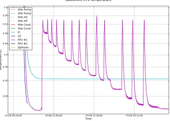
The Focal Plane Unit # 1 [FPU # 1], which the detectors rest on, was cooled overnight to its lowest value of approximately 250mK. The measurement system was calibrated, and if the readout component (the SQUID attached to a given detector failed, this was noted (no data was taken for these detectors). Then, for each temperature of interest, the detectors were briefly heated to “unlatch” them before data was taken.
Exterior heating was necessary because when the TES goes far enough below its critical temperature and becomes superconducting (as it is at 250mK), its resistance becomes extremely low, and so Joule dissipation has little effect on the tempera-ture. Thus, simply increasing the current through the device has little effect on the resistance of the TES up to a certain critical current that heats it enough to bring it from its low temperature into the transition region, and the critical current needed for detectors at 250mK is too high to practically run through the detectors. So the entire FPU # 1 was heated until the detectors were hot enough for it to be practical to apply the critical current (“zap” the detector) to pull them out of their “latched superconducting” state, past the superconducting transition region and into being simply normal resistors. Then a smaller constant bias was applied to keep them above the transition as the FPU # 1 was allowed to cool.
07/28 08:24:00 07/28 12:00:00 07/28 15:36:00 07/28 19:12:00 Time
[image:31.612.123.475.90.340.2]0.28
Figure 3.1: FPU # 1 temperature during the successful data-taking run is in pink. Note that the temperature of the detectors exceeds the FPU # 1 plane during the application of the critical current (“zapping”) that occurred at the top of each peak, and for some time thereafter as data was taken.
[image:31.612.119.374.453.653.2]Calibration
The readout circuit for IT E S on each detector is only correct up to an offset. The actual magnitude of the currents is relevant for power versus resistance calculations, so the data is calibrated using the fact that the TES becomes a normal resistor at sufficiently high temperatures. At such temperatures, as are apparent in Fig. 3.2 from at least higher than 8000 DAC, the detector has a constant resistance value.
Referring to the circuit as documented in Fig. 3.3, each branch must have voltage
Rshunt∗ (Ibias −IT E S). Thus by Ohm’s law RT E S = Rshunt ∗ (Ibias− IT E S)/IT E S =
Rshunt∗ (Ibias/IT E S−1).
The value ofIbias/IT E S was read by fitting a line to a region where the detector was a normal resistor, as enclosed by the dashed green lines displayed on the calibrated IV curves such as Fig. 3.4. This line’s offset (the value displayed next to ’Off’ at the bottom of the IV curves) was subtracted from the raw data to calibrate the offset, as per Ohm’s law; this calibrated data is displayed in the IV plots shown henceforth. TheIbias/IT E Swas used to calculate the normal resistance (Rn value) of the detector as described above. The average Rn over the different temperatures is displayed at the top left of the IV curves. If this average Rn was outside the range of 30-150 milliOhms, the plot was said to have "Failed the Rn cuts", because such slopes are highly unlikely to have come from functional detectors. In this data set, all such failures were unmistakably not following the typical TES IV curve. For example, many E and G types failed in the same manner as illustrated in Fig. 3.4.
Differences in Aluminum IV curve data acquisition
There was one important limitation on the Al IV curves: the bias needed reach the Aluminum normal region was beyond the equipment’s capacity (though it could get high into the transition).
3.2 Superfast data acquisition
Superfast refers to taking data faster than normal ( 200 kHz as opposed to the 1 kHz science data taking rate). This is made possible by only taking data for one row of detectors at a time, enabling the machinery to more quickly cycle through all of its target detectors. The point is to map the detector response in the frequency domain, which is important for analyzing noise and detecting any issues with aliasing. In superfast data acquisition, the detectors were unlatched as with the IV curves, and then fed a steady DC bias current.
3.3 Bolometer impedance acquisition
To explore the mechanism of instability seen in the IV curves, we measured the electrical impedance of the bolometers.
C h a p t e r 4
METHODS: ANALYSIS
4.1 Titanium TES
The Titanium TES is the main science detector, used for making measurements. After the IV curves were taken and the data was calibrated, the current data was used to construct Power-Resistance plots, as seen in the right side of several previous figures (e.g. Fig. 2.6, 2.7). This was done to find the in-transition region more easily and in accordance with the theory on superconductor transition curves (reminder in Fig. 4.1). In practice the measuring equipment is prone to difficulties and erratic behavior once the TES is too far into the superconducting zone (acceptable because while measuring science data it should not enter it), hence why the superconducting sections of our PR plots differ from theory.
[image:34.612.116.318.444.646.2]Selecting the in-transition region from the PR plots was nontrivial. Picking the tran-sition by hand was not feasible for the 1664 different detector-temperature combina-tions. The initial algorithm relied on a hardcoded difference in standard deviation between the next and previous 10 points. As illustrated in Fig. 4.2, this algorithm
Figure 4.2: A particularly bad column (mce column 3) of Algorithm 1 (local standard deviation change) PR plot results for the 254 mK run. Consider, for example, the row 9 detector. Blank plots has failed or absent detectors, or failed SQUIDS.
was insufficiently accurate due to large differences in noise levels between detectors.
Several iterations occurred between the first and the final, successful algorithm for cutting the titanium transitions (it was successful on all but 4 detectors, which were then set by hand inspection). For comparison the final algorithm produced the cuts in Fig. 4.3
Figure 4.3: The same column algorithm 1 failed on, much improved in the final algorithm.
4.2 Aluminum TES
The aluminum TES is primarily used for calibration and testing under a 300 K background due to its higher saturation power [1].
The Aluminum also had some issues with plotting PR cuts that were eventually resolved. For Aluminum PR transition cutting algorithm code please contact the author.
Basic Statistical Methods for modeling
Figure 4.4: These residuals are small compared to the actual values.
are plotted below for the model detector in Fig. 4.4. The errors are two to three orders of magnitude less than the values of the points they bound. Running the fits with an additional sigma parameter did not significantly affect the shape of the best fit.
These errors were then used to find an initial starting estimate for various model parameters, which were then run through a 1 million point Markov Chain Monte Carlo to estimate a best fit and uncertainties. The resultant best fit was then taken as the new starting guess for another derivative-seeking optimal estimation in order to get the final best fit parameters. The percent of best fit parameters that were selected this way to lie within the error bounds determined by the MCMC is referred to as the optimal capture; optical capture < 100% was taken as a sign that convergence had not occurred and more steps were necessary (in all cases, enough steps did guarantee 100% optimal capture).
4.3 Superfast
The basic analytical approach is to perform a Fourier transform to see the noise at different frequencies. Detailed analysis of the superfast data beyond this has not yet been prioritized.
4.4 Impedance
electrical bandwidth of the readout, and thermal decoupling.
R = TES resistance
Lnyq = 0.7e-6 H
Rsh = 0.003 Ohm
b = L0/gamma
eps = Rsh / R
taue = Lnyq / R
t0 = -1j*(-1 + b + L0) + (-1 + b)*w*tau0
t1 = 1j*(1 + b + L0 + eps - (b+L0)*eps)
t2 = (-1 + b*(-1+eps)-eps)*tau0*w
t3 = taue*w*(-1+b+L0+1j*(-1+b)*tau0*w)
Y = (1.0/R) * t0 / (t1 + t2 + t3)
Fit parameters:
gamma: Ratio of internal thermal conductivity to leg thermal conductivity. Higher is better.
loopgain L0: Ratio of electrothermal feedback to leg thermal conductivity. Zero for a resistor, infinite for an ideal TES.
R/Rn: Fraction of normal resistance. Measure of depth in transition.
tau0 or f3db0: Ratio of island heat capacity to leg thermal conductivity. Speed of detector at zero loopgain.
Like the standard model for the ideal TES, this has two time dependent degrees of freedom, the current in the TES and the temperature of the island.
The difference is that the TES temperature (TT E S) can heat above the temperature of the island (Tisland) through electrical power dissipated in the TES (Pe) flowing
through the decoupling link (γG):
TT E S =Tisland +
Pe
γG (4.1)
All the bias points for one bolometer are fit simultaneously, with a single value for
estimate the range over which the detector is in transition by placing a criterion on the flatness of the PR curve, and looking at the difference between the normal resistance and the highest resistance where the detector is unstable.
Transition range graphs
Table 5.1 displays the critical metrics for simultaneous operation of columns of detectors derived from the data for all detector types. Figures 5.1 and 5.2 plot the transition ranges of detector types A and F and illustrate the derivation of the critical metrics. The voltage bias in the table has units of microamps of current applied to the 3mΩshunt resistor.
While the few E and G types that passed the normal resistance cuts had long mean lengths, their yields were very low, and most of their failures displayed an IV pattern unique to these types. These are the types that had vias down to the titanium to make direct electrical contact. The D and F types on the other hand had high yield,
Table 5.1: Detector Stats
Det. Det. Max Det. Best Best Bias Mean type yield1 Simultaneously Bias Region Length Length
Biased2 [µA] [µA] [µA]
A 83 67 317 14 105
B 88 69 280 4 100
C 92 83 280 29 120
D 93 93 247 93 170
E 46 46 246 128 190
F 100 100 225 100 169
G 31 31 272 166 178
1 1.5 2 2.5 3 3.5 4 4.5 5
I-bias [A] 10-4
0 5 10 15 20 25 30 35 mceRow E7Dark,temp254,dType:A
det yield: 83.3%
MaxDetBiased: 66.7%
1 1.5 2 2.5 3 3.5 4 4.5 5
I-bias [A] 10-4
0 5 10 15 20 25 30 35 Ndets
Ndet well biased
Best Bias (BB): 0.000317 [A]
[image:40.612.108.507.80.308.2]BB Region Length: 1.43e-05 [A]
Figure 5.1: Type A transition range graph at a bath temperature of 254mK. The x axes are the current applied to the TES shunt resistors. The vertical line shows the optimal current where the largest number of detectors are operating simultaneously. In the left plot, horizontal bars show the limits of the in transition for each detector of type A. The right plot shows the count of in transition detectors for each bias current.
1 1.5 2 2.5 3 3.5 4 4.5 5
I-bias [A] 10-4
0 5 10 15 20 25 30 35 mceRow E7Dark,temp254,dType:F
det yield: 100%
MaxDetBiased: 100%
1 1.5 2 2.5 3 3.5 4 4.5 5
I-bias [A] 10-4
0 5 10 15 20 25 30 35 Ndets
Ndet well biased
Best Bias (BB): 0.000225 [A]
BB Region Length: 9.96e-05 [A]
[image:40.612.109.505.438.664.2]perature (in mK). Higher is better. Types A, B, C and H increase in stability with temperature while the others do not, consistent with decreasing loopgain allowing them to satisfy the thermal stability criterion that D,E,F,G have already met.
and very wide biasable regions, without the characteristic instability of the baseline A-type detectors. The D and F types have no direct electrical contact between palladium-gold and titanium, indicating that the limiting thermal resistance in the A-type is the silicon nitride island thickness, and the electron-phonon relaxation time in our titanium may be shorter than 1-3 microseconds.
5.2 Aluminum PR Slope Models and Fit Results
One plausible explanation for the slope is that, instead of a normal transition curve, phase separation is occurring in the TES due to our Aluminum TES’s relatively long length; Anderson et al. suggests that this effect would occur to some extent in our
detectors [2]. Then instead of a TES in transition (see Fig. ??), we have part of a TES superconducting (electrical resistance 0) and the other part normal (electrical resistance Rn). Thus, the total thermal resistance from the TES to the island should be inversely proportional to the resistance for the TES in the apparent “transition” region: as the normal, electrically resistive, heat-conducting region expands, the surface area of it increases and thus the total thermal conductance increases.
Fourier’s law gives that Pt hermal = Pt h = (TT E S˘Tbat h)/Rt hermal = Pelectrical = Pel
in electrothermal equilibrium. The thermal resistance comes from two thermal resistances in series: the thermal resistance of the TES to the island it rests on, and the thermal resistance of the island’s legs that connect to the bath. The temperature of the bath was constant; we model the temperature of the TES as constant at the Aluminum critical temperature (1.5 K) as well, andTbat hwas measured at 433 mK. This gives Eq. 5.1, for the Aluminum phase separation model:
P= (TT E S−Tbat h)
(Rleg+ Runknown∗ (Rn/Relectrical)) (5.1)
Setting (Runknown∗Rn) as one parameter and fitting the transition region with MCMC and optimal estimation techniques, we obtain the red fit in Fig. 5.5 to the blue data (with error bars). The fit gaveRleg =2.12874e+9[W/K]in[2.12867e+9,2.12877e+ 9]with 0.68 confidence, andRunknown∗Rn= 8.46910e+7[W2/K2]in[8.46743e+ 7,8.46876e+7]with 0.68 confidence. This fit had a reduced Chi-squared of 9205.
Another possible refinement is considering the possibility of a two-stage temperature system, which was the source of the problem with the titanium but was not expected to be problematic at the aluminum TES’s higher temperature. In this system, the island sits at a different temperature, T, from the bath or the TES. The island legs have a 3.5 exponent temperature dependence relation [1], resulting in this system of equations:
P= (Relectrical
Rn ) ∗GT E S−island ∗ (Tcritical−Tisland) (5.2)
P=Gisland−bat h∗ (Tislandn −T n
bat h) (5.3)
Figure 5.5: The two main models attempted, with fits given for a sample A-type detector.
same amount of heat power in total was flowing everywhere at any one time. These equations can be solved numerically (and for n= 3.5 must be solved numerically) for the island temperature, which can then be plugged in to model P.
The computational cost of getting the numerical roots was prohibitive for a million point MCMC run or even a 100,000 point run, which was typically the minimum needed for optimal capture. Thus we employed another common estimation and fit to the analytically solvable n=3 case instead. Results are given by the green fit in Fig. 5.5. GT E S−island/Rn= 2.99890e-8 [W/(K Ohm)] in [2.99865e-8, 2.99923e-8] with 0.68 confidence. Gisland−bat h= 2.21218e-10 [W/K] in [2.998654e-8, 2.999235e-8] w/ 0.68 confidence. Reduced Chi-squared of 8101.
A line on this data, in comparison, has a reduced Chi-squared of 708, suggesting that the model is deeply flawed. The line fit is given in Fig. ??, and the line likelihood density and histogram of points are given in Figs. ?? and ?? as examples of the error computations performed and the checks for MCMC validity, which were done for all fits.
Figure 5.6: The best fit of a line to the A type detector, which had no currently known physical motivation.
Figure 5.8: The histogram of MCMC point values of the best fit of a line to the A type detector. This is an important check on the validity of MCMC, which requires that parameters are roughly gaussian in likelihood distribution.
best fit line, which was still unquestionably off to the eye. We tried varying n in the two-stage model, in the range n = [0.5, 4]. 22 different 100,000+ step fits were performed and none of them looked remotely close. The line was the closest but unlike every other model attempted has no physical motivation and thus provides no useful information about device properties.
5.3 Superfast preliminary results
Figure 5.9: Fourier analysis of A-type detector for various current biases in DAC; amplitude vs. frequency. Note the "bump" of increase in frequency amplitude a bit bast 104.
[image:46.612.121.419.410.650.2]Figure 5.11: Fourier analysis of D-type detector for various current biases in DAC; amplitude vs. frequency. Note the lack of a "bump" of increase in frequency amplitude a bit bast 104.
5.4 Impedance
Figure 5.12: Fitted admittance for representative type A (top) and F (bottom) bolometers. Points are measured data, one point per frequency, lines are fits to the model. Color shows the bias voltage. Data is shown down to the lowest bias voltage where the detector remained stable.
be increased by a factor of 2-3 by bringing the heat capacity metal closer to the TES film. The stabilized detectors better accommodate variations in optical load and detector properties, in principle allowing a multiplexed column of detectors to be operated at a single bias voltage with higher on sky yield.
While we have ruled out all cases in which phase-separation is the primary cause of the Aluminum’s in-transition slope, and have similarly discarded the two-stage system as primarily relevant, the cause of the large slope in the Aluminum transition remains unclear. There are still a few unexplored possibilities. It is possible that TES temperature did vary significantly, that a nontrivial gradient exists between the two phase separated regions, that the TES critical temperature is current-dependent, and/or that Fourier’s law is also incorrect for the mode of thermal transport in the normal region. While these effects were projected to be relatively small, further investigation into these possibilities will be taken.
BIBLIOGRAPHY
[1] P. A. R. Ade and et. al. et. “Antenna-Coupled Bolometers used in BICEP2, KECK ARRAY, and SPIDER”. In: The Astrophysical Journal(2015). url:
http://arxiv.org/pdf/1502.00619.pdf.
[2] AJ Anderson et al. “Modeling phase-separated transition-edge sensors in SuperCDMS detectors”. In:arXiv preprint arXiv:1109.3620(2011).
[3] D. A. Bennett et al. “A Two-Fluid Model for the Transition Shape in Transition-Edge Sensors”. In:Journal of Low Temperature Physics167.3 (May 1, 2012), pp. 102–107. issn: 1573-7357. doi: 10.1007/s10909-011-0431-4. url:
https://doi.org/10.1007/s10909-011-0431-4.
[4] Keck Array Collaboration BICEP and PAR Ade. “BICEP2/Keck Array VI: Improved Constraints On Cosmology and Foregrounds When Adding 95 GHz Data From Keck Array”. In:arXiv preprint arXiv:1510.09217(2016).
[5] C. Eller. Building BICEP2: A Conversation with Jamie Bock. Web Page. 2014. url: http : / / www . caltech . edu / news / building bicep2
-conversation-jamie-bock-42306.
[6] E. M. George and et al et. “A Study of Al-Mn Transition Edge Sensor Engi-neering for Stability”. In:Journal of Low Temperature Physics176.3 (2014).
doi: 10.1007/s10909- 013- 0994- 3. url:https://arxiv.org/abs/
1311.2245.
[7] M. E. Gershenson et al. “Millisecond electron–phonon relaxation in ultrathin disordered metal films at millikelvin temperatures”. In:Applied Physics Let-ters 79.13 (Sept. 2001), pp. 2049–2051. issn: 0003-6951, 1077-3118. doi:
10 . 1063 / 1 . 1407302. url: http : / / aip . scitation . org / doi / 10 .
1063/1.1407302(visited on 12/11/2017).
[8] J. M. Gildemeister. “Voltage-Biased Superconducting Bolometers for Infrared and mm-Waves”. Ph.D. thesis. University of California, Berkely, 2000.
[9] W. Holmes et al. “Measurements of thermal transport in low stress silicon nitride films”. In: Appl. Phys. Lett.72.18 (Apr. 1998), pp. 2250–2252. issn: 0003-6951. doi: 10 . 1063 / 1 . 121269. url: http : / / aip . scitation .
org/doi/10.1063/1.121269(visited on 08/24/2017).
[10] W. Hu.CMB Tutorial - Polarization - Gravitational Waves. Web Page. 1996.
url: http : / / background . uchicago . edu / ~whu / intermediate /
Polarization/polar6.html.
978-3-540-20113-and-sensitivity-of-the-Keck-array/10.1117/12.926934.short
(visited on 12/11/2017).
[14] Mark A. Lindeman et al. “Impedance measurements and modeling of a transition-edge-sensor calorimeter”. In:Review of Scientific Instruments75.5 (Apr. 2004), pp. 1283–1289. issn: 0034-6748. doi: 10.1063/1.1711144.
url: http : / / aip . scitation . org / doi / abs / 10 . 1063 / 1 . 1711144
(visited on 12/11/2017).
[15] Dan McCammon. “Thermal equilibrium calorimeters–an introduction”. In: Cryogenic particle detection. Springer, 2005, pp. 1–34.
[16] Planck Collaboration. “Planck intermediate results. XXX. The angular power spectrum of polarized dust emission at intermediate and high Galactic lat-itudes”. In: Astronomy & Astrophysics 586 (Feb. 2016). arXiv: 1409.5738, A133. issn: 0004-6361, 1432-0746. doi:10.1051/0004-6361/201425034.
url:http://arxiv.org/abs/1409.5738(visited on 11/15/2017).
[17] P. L. Richards. “Bolometers for infrared and millimeter waves”. In: Journal of Applied Physics 76.1 (1994), pp. 1–24. doi: 10.1063/1.357128. url:
http://aip.scitation.org/doi/abs/10.1063/1.357128.
[18] P Santhanam and DE Prober. “Inelastic electron scattering mechanisms in clean aluminum films”. In:Physical Review B29.6 (1984), p. 3733.
[19] Jian Wei et al. “Ultrasensitive hot-electron nanobolometers for terahertz as-trophysics”. In: Nat Nano 3.8 (Aug. 2008), pp. 496–500. issn: 1748-3387.
doi:10.1038/nnano.2008.173. (Visited on 08/24/2017).
[20] Adam L Woodcraft et al. “Thermal conductance measurements of a silicon nitride membrane at low temperatures”. In: Physica B: Condensed Matter 284-288.Part 2 (July 2000), pp. 1968–1969. issn: 0921-4526. doi:10.1016/
S0921 - 4526(99 ) 02925 - 7. url: http : / / www . sciencedirect . com /
A p p e n d i x A
TITANIUM SAMPLE IV, PR AND TRANSITION-SELECT
PLOTS FOR ALL TYPES
A.1 Characteristic IV plots
Fig.A.1 is typical of a functional type A, the original detector type. Observe how the instability, most prominent at low temperatures, shortens the available operating range of the detectors.
Fig.A.2 is typical of a functional type B detector, which added PdAu to the aluminum TES. It is quite similar to type A.
Fig.A.3 is typical of a functional type C detector, which had a PdAu finger and a via on the aluminum TES. While the instability is seemingly greatly diminished, the transition range still drops off at lower temperatures. The oddities in the supercon-ducting region are due to a quirk of the readout electronics.
Fig.A.4 is typical of a functional type D detector, which had a PdAu finger on the titanium TES.
Fig.A.5 is typical of a functional type E detector, which had a PdAu finger and a via on the titanium TES. Note that many of the type E detectors failed the Rn cuts.
Fig.A.6 is typical of a functional type F detector, which coated the titanium and aluminum TES’s in PdAu.
Fig.A.7 is typical of a functional type G detector, which coated the titanium and
0 2 4 6 8
Ibias [Amps] 10-4
-8 -6 -4 -2 0 2 4 6 8 10 12 Ites [Amps] 10-5 Rn: 73.76 m
0 50 100 150 200
TES R [m ] 0 2 4 6 8 10 12 14 16 18 20
TES P [pW]
254 259 273 297 320 334 350 368 380 404 429 443 480
0 2 4 6 8 Ibias [Amps] 10-4
-4 -3.5 -3 -2.5 -2 -1.5 -1 -0.5 0 0.5 Ites [Amps] 10-4
Rn: 63.24 m
Off: 0.00015106 Amps
0 50 100 150 200 TES R [m ]
0 2 4 6 8 10 12 14 16 18 20
TES P [pW]
254 259 273 297 320 334 350 368 380 404 429 443 480
Figure A.3: Type C characteristic IV plot.
0 2 4 6 8
Ibias [Amps] 10-4
-10 -8 -6 -4 -2 0 2 4 6 8 Ites [Amps] 10-5
Rn: 64.86 m
Off: 5.6727e-05 Amps
0 50 100 150 200 TES R [m ]
0 2 4 6 8 10 12 14 16 18 20
TES P [pW]
254 259 273 297 320 334 350 368 380 404 429 443 480
0 2 4 6 8 Ibias [Amps] 10-4
-5 0 5 10 Ites [Amps] 10
Rn: 81.47 m
Off: 2.931e-05 Amps
0 50 100 150 200 TES R [m ]
0 2 4 6 8 10 12 14 16 18 20
TES P [pW]
254 259 273 297 320 334 350 368 380 404 429 443 480
Figure A.5: Type E characteristic IV plot.
0 2 4 6 8
Ibias [Amps] 10-4
-8 -6 -4 -2 0 2 4 6 8 10 Ites [Amps] 10-5
Rn: 70.14 m
0 50 100 150 200
TES R [m ] 0 2 4 6 8 10 12 14 16 18 20
TES P [pW]
254 259 273 297 320 334 350 368 380 404 429 443 480
Figure A.6: Type F characteristic IV plot.
0 2 4 6 8
Ibias [Amps] 10-4 -8 -6 -4 -2 0 2 4 6 8 10 Ites [Amps] 10-5
Rn: 74.06 m
Off: 4.4899e-05 Amps
0 50 100 150 200 TES R [m ]
0 2 4 6 8 10 12 14 16 18 20
TES P [pW]
254 259 273 297 320 334 350 368 380 404 429 443 480
Figure A.7: Type G functional characteristic IV plot.
aluminum TES’s in PdAu and had a via on the titanium TES. Note that many of the type G detectors failed the Rn cuts.
A.2 PR transition-select plots
[image:55.612.108.353.473.691.2]Figures A.9, A.10, A.11, A.12, A.13, A.14, A.15, and A.16 illustrate the algorithm used to select the start and end of the usable transition range. The green lines mark the start (high end) of the transition range and the red lines mark the end (low end) of the transition range. They also display the pr plots for all functioning detectors of each type, for comparison. Note that some detectors did not have data taken due to failures of the readout system unrelated to the detectors, so simple number of plots is not equivalent to the detector yield.
Figure A.10: Type B PR transition-select graph at 254mK.
[image:56.612.109.353.437.654.2]Figure A.12: Type D PR transition-select graph at 254mK.
[image:57.612.111.350.434.654.2]Figure A.14: Type F PR transition-select graph at 254mK.
[image:58.612.109.353.436.653.2]Figure A.16: Type H PR transition-select graph at 254mK.
A.3 Transition range graphs
Figures A.17, A.18, A.19, A.20, A.21, A.22, A.23, and A.24 display the critical metrics derived from the data. The first is detector yield, the percent of detectors of each type that displayed functional IV curves, not considering detectors where the readout system failed during tuning for reasons unrelated to the detectors.
Figure A.18: Type B transition range graph at 254mK.
Figure A.20: Type D transition range graph at 254mK.
Figure A.22: Type F transition range graph at 254mK.