Rochester Institute of Technology
RIT Scholar Works
Theses Thesis/Dissertation Collections
2008
Development, fabrication, and characterization of a
vertical-diffused MOS process for power RF
applications
Kazuya TokunagaFollow this and additional works at:http://scholarworks.rit.edu/theses
This Thesis is brought to you for free and open access by the Thesis/Dissertation Collections at RIT Scholar Works. It has been accepted for inclusion in Theses by an authorized administrator of RIT Scholar Works. For more information, please [email protected].
Recommended Citation
Development, Fabrication, and Characterization of a
Vertical-Diffused MOS Process for Power RF Applications
By
Kazuya Tokunaga
A Thesis Submitted
in Partial Fulfillment
of the Requirements for the Degree of
Master of Science
in
Microelectronic Engineering
Approved by:
Prof. ___________________________________ Dr. Karl D. Hirschman (Primary Thesis Advisor)
Prof. ___________________________________ Dr. Michael A. Jackson (Thesis Advisor)
Prof. ___________________________________ Dr. Christopher R. Hoople (Thesis Advisor)
Dr. Jere Hohmann (External Collaborator) Mr. Benedict Caccavale (External Collaborator)
DEPARTMENT OF MICROELECTRONIC ENGINEERING
COLLEGE OF ENGINEERING
ROCHESTER INSTITUTE OF TECHNOLOGY
ROCHESTER, NEW YORK
Development, Fabrication, and Characterization of a
Vertical-Diffused MOS Process for Power RF Applications
By
Kazuya Tokunaga
I, Kazuya Tokunaga, hereby grant permission to the Wallace Memorial Library of the Rochester Institute of Technology to reproduce this document in whole or in part that any reproduction will not be for commercial use or profit.
___________________________ ________________________
Acknowledgment
I would like to thank all people who have helped and inspired me during my
thesis study. I want to give thanks to my primary advisor, Dr. Karl D. Hirschman, for his
assistance, support, and guidance during my research and study at Rochester Institute of
Technology. Deepest gratitude is also due to the members of the supervisory committee,
Dr. Michael Jackson and Dr. Christopher Hoople; without their knowledge and assistance
this study would not have been successful. I would also like to express thanks to the
people from Spectrum Devices, Dr. Jere Hohmann and Mr. Benedict Caccavale, for their
technical and financial support.
I would like to thank the faculty of the Microelectronic Engineering Department
and the staff of the Semiconductor & Microsystems Fabrication Laboratory for their
continuous support. All colleagues at the Microelectronics Engineering made it a friendly
place to work. In particular, I would like to thank Germain Fenger and Ward Johnson for
their friendship and help in the past years.
Lastly and most importantly, I wish to express my love and gratitude to my
Abstract
High power radio frequency (RF) applications have become important because of
a growing demand from the wireless market. With their superior switching speed, power
Metal-Oxide-Semiconductor Field Effect Transistors (MOSFETs) have become one of
the well-known technologies used in high power RF systems. The primary focus of this
thesis work was the development, fabrication, and characterization of discrete
Vertical-drain lateral-Diffused MOS (VDMOS) power transistors using an interdigitated
source/gate design. Several types of high power devices were also presented for
comparison to the VDMOS structure. This thesis describes the overall purpose and the
objectives of the proposed project, and provides the methodology used to complete these
objectives. This project supports a new development initiative of the project sponsor,
Spectrum Devices, Inc., who has been working with RIT in power bipolar technologies
over the last two years.
The process steps to create a 50 V power VDMOS transistor structure were
designed using Silvaco ATHENA (SUPREM-IV) process simulation. Typical power
VDMOS transistor fabrication steps were used as a starting point with modifications to
include Faraday and UIS implant steps to address certain parasitic effects. The Faraday
shield implant was performed to shift the parasitic gate- field capacitance over to the input
side of the device, which should dramatically improve the frequency response of the
device. The UIS implant was used to reduce the parasitic BJT of a power VDMOS
transistor. The implementation of the proposed structure also eliminated the need for an
added masking operation for each implant step, and kept the structure self- aligned to the
in photolithography steps. The initial process parameters were carefully varied and
adjusted to meet the target specifications (such as threshold voltage, breakdown voltage,
gate oxide thickness, etc.) using ATHENA and ATLAS simulation software.
After the device fabrication was completed, DC testing was performed on the
fabricated VDMOS transistors both at RIT and at Spectrum Devices. A successful
extraction of the transfer curves, family of curves, and breakdown voltage plots both in
low and high current settings was achieved. The designed process produced a power
VDMOS with a breakdown voltage of up to 180 V, a threshold voltage of ~3.8 V, a
transconductance up to ~7 mhos, and an operating current of nearly 5 A. The
experimental results were compared to the target specification provided by Spectrum
Devices. In addition, impacts of the Faraday shield implant on the breakdown voltage and
terminal capacitances of a VDMOS device were verified through DC testing. Preliminary
wafer- level AC testing was performed and demonstrated the functional performance of
the device up to 100 kHz frequency range. Although it would be interesting to see the
impact of UIS implant step on a device performance, no AC test was yet to be performed.
This work presented the first power VDMOS transistors successfully fabricated
and characterized at RIT. With the data and information obtained from this thesis project,
Table of Contents
Title Page ...i
Library Release ...ii
Acknowledgment ...iii
Abstract ...iv
Table of Contents...vi
List of Tables ...ix
List of Figures ...xi
List of Symbols, Units and Acronyms... xviii
1. Introduction and Motivation ...1
1.1 Introduction... 1
1.2 Advantages, Disadvantages, and Characteristics Comparison with BJT... 2
1.3 Conventional MOSFET vs. Power MOSFET... 7
1.4 Development of Power MOS Devices... 8
1.5 Thesis Goal and Objective ... 11
1.6 Thesis Outline ... 12
2. Theory...14
2.1 Device Characteristics: Static Operation ... 14
2.2 Threshold Voltage... 16
2.3 Typical Output ... 18
2.4 On Resistance... 19
2.5 Breakdown Voltage... 22
2.7 VDMOS: Capacitive Elements & Dynamic Behavior... 27
2.8 VDMOS Parasitic BJT... 31
2.9 Conventional VDMOS Process Flow [7] ... 33
3. Process Design and Simulation...38
3.1 Substrate Selection... 38
3.2 ATHENA and ATLAS Simulation... 39
3.3 Mask Layout ... 45
4. 50 V VDMOS Fabrication...51
4.1 UIS Implant Blocking Test ... 51
4.2 Nitride Stress Test... 53
4.3 VDMOS Lot 1... 54
5. Electrical Characterization...83
5.1 Testing Overview... 83
5.2 Testing Equipment ... 84
5.3 Electrical Test ... 87
5.3.1 Transfer curve (VT sweep)... 88
5.3.2 Output characteristic curve (Family of Curves)... 92
5.3.3 Breakdown voltage test... 95
5.3.4 Transconductance... 98
5.3.5 Zero gate voltage drain current ... 100
5.3.6 Resistive / Capacitive Load Test... 101
5.3.7 UIS implant AC (High Frequency) Test... 103
5.3.9 Failure Analysis ... 104
6. Conclusion ...107
7. References ...111
List of Tables
Table 1.1. The characteristic comparison of BJT and MOSFET [2]. 2
Table 3.1. The parameters used for the VDMOS process design. 40
Table 3.2. Target specifications and simulated results. 41
Table 4.1. Detailed information of the wafers used for Lot 1. 55
Table 4.2. Detailed information of the monitor wafers used for Lot 1. 55
Table 4.3. Design of Experiment performed for the first lot. 56
Table 4.4. Standard RCA Clean steps used [24]. 56
Table. 4.5. Properties of silicon nitride prepared by PECVD and LPCVD. Adapted from
[25]. 65
Table 5.1. Testing equipment comparison (advantages and disadvantages). 87
Table 5.2. The threshold voltage extracted from the transfer curves. 92
Table 5.3. BVDSS values extracted from Fig. 5.17. 97
Table 5.4. The transconductance extracted from the family of curves (low current). 98
Table 5.5. The transconductance values extracted from the family of curves (high current).
98
Table 5.6. gfs values extracted from Fig. 5.18. 99
Table 5.7. IDSS values extracted from Fig. 5.19. 100
Table 5.8. The rise time and fall time of VDMOS transistors in a resistive load /
capacitive load condition. 102
Table 5.9. The implant block stack thickness measurements taken on VI-01-09 wafer
layer using LAM490. The color in the parenthesis describe the color of the
etched area under microscope. 105
Table 5.10. Table showing the threshold voltage shift due to boron implanting through
the implant block stack. 106
Table 6.1. Device results compared to device target specifications given in [11]. The gray
shaded numbers represent results that did not meet the target specification
List of Figures
Fig. 1.1. Plot of device current rating vs. device voltage rating for solid state power
device applications. Adapted from [1]. 1
Fig. 1.2. Driving circuits for a typical (a) BJT and (b) power MOSFET [7]. 3
Fig. 1.3. The safe operating area (SOA) of BJT and MOSFET device. Reduced
performance of BJT (dotted line) due to the second breakdown limit can be
seen [7]. 5
Fig. 1.4. Maximum current and breakdown (hold-off) voltage limitations faced with MOS
transistors and BJTs [3]. 6
Fig. 1.5. The cross-sectional view of a conventional MOS transistor. Simply scaling up
this structure will not work to be used for power applications [7]. 7
Fig. 1.6. The cross-sectional view of a VMOSFET. An anisotropic etch is used to
produce a V-shaped groove in the semiconductor surface [6]. 9
Fig. 1.7. The cross-sectional view of a truncated VMOSFET. The current crowing can be
reduced using this structure [7]. 9
Fig. 1.8. The cross-sectional view of a LDMOS [7]. 10
Fig. 1.9. The cross-sectional view of a VDMOS [7]. 11
Fig. 2.1. The four types of MOS transistor operating regions with their circuit symbols
and capacitance-voltage (C-V) characteristics [7]. (a) n-type enhancement mode.
(b) n-type depletion mode. (c) p-type enhancement mode. (d) p-type depletion
mode. 15
Fig. 2.2. The cross sectional view of a VDMOS transistor showing the active region [7].
Fig. 2.3. The process of a channel formation. (a) and (b) shows the depletion region
formation, whereas (c) shows the formation of the inversion layer [6]. 16
Fig. 2.4. The effect of NA and Qox on VT at room temperature [7]. 17
Fig. 2.5. The typical output characteristic of a VDMOS transistor in n-channel,
enhancement mode modified by adding points A, B, and C for discussion in
text [12]. 18
Fig. 2.6. A VDMOS transistor showing its internal resistances (RDS(on)) [6]. 20
Fig. 2.7. The relative importance of each of the components to RDS(on) for different
voltage ratings. REPI from this reference is RD0 component in Equation 2.4. Rn+
is included in Rwcml. Rwcml is sum of bond wire, contact, metallization and lead
frame resistance [3]. 21
Fig. 2.8. Dependence of the junction temperature to RDS(on) [4]. 22
Fig. 2.9. BVDSS vs. doping concentration density and thickness of n- epilayer [14]. 24
Fig. 2.10. BVDSS vs. RD(on) for commercially available power MOS transistors, showing
the design tradeoff [15]. 25
Fig. 2.11. The internal capacitances of a power MOS device [17]. 28
Fig. 2.12. The cross-sectional view of a VDMOS (a) without the Faraday shield implant
and (b) with the Faraday shield implant. The diffusion layer is connected to the
source region and acts as a conductor between the gate and the drain substrate,
eliminating the effect of Cgd. 30
Fig. 2.13. The cross-section of a power VDMOS showing a parasitic BJT [7]. 31
Fig. 3.1. A two-dimensional profile of a VDMOS structure showing three different
terminals and different diffusion regions simulated using ATHENA 41
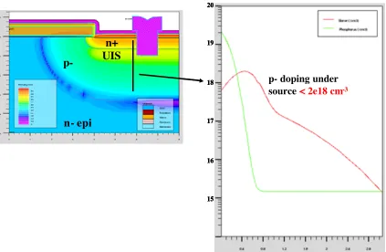
Fig. 3.2. ATHENA simulation result showing the p- doping concentration under the
source region for the structure without a UIS implant step. 42
Fig. 3.3. ATHENA simulation results showing the p- doping concentration under the
source region for the structure with a UIS implant step. 43
Fig. 3.4. ID-VG characteristic curves of simulated VDMOS structures with and without
UIS implant. 44
Fig. 3.5. The family of curves of a simulated VDMOS structure with the UIS implant. 44
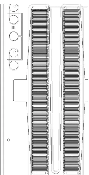
Fig. 3.6. The mask layout of a VDMOS structure showing two segments of a device.
Each segment consists of 66 individual cells. 46
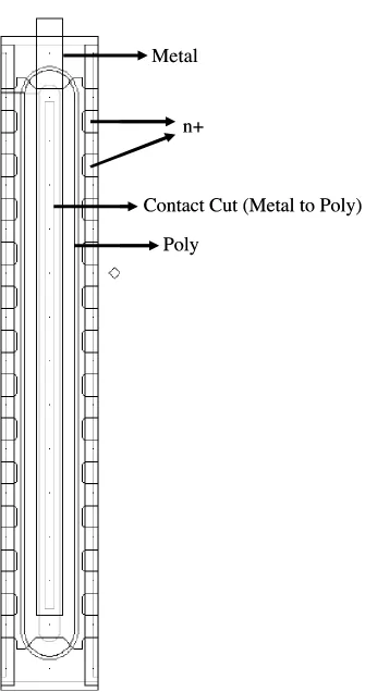
Fig. 3.7. The mask layout of a cell of the VMOS structure. 47
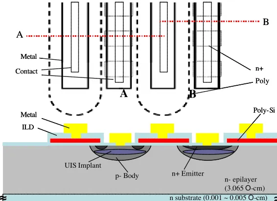
Fig. 3.8. The cross-section of a proposed structure. The device on the left side shows the
cross-section portion formed by line A, whereas the device on the right side
shows the cross-section portion formed by line B. 49
Fig. 3.9. The 3-D cross-section of a proposed structure showing a metal line shorting p-
body and n+ source regions. 49
Fig. 4.1. Parameters used in SRIM. 51
Fig. 4.2. The boron ion distribution of the proposed implant block stack (600 nm Nitride /
50 nm TEOS SiO2 / 600 nm polysilicon) using the implant energy of 300 keV
Fig. 4.3. The boron ion distribution of the proposed implant block stack (600 nm Nitride /
50 nm TEOS SiO2 / 600 nm polysilicon) using the implant energy of 300 keV
and the implant dose of 1x1014 cm-2 simulated in ATHENA. 53
Fig. 4.4. A cross-section through the device after the first field oxide growth. 57
Fig. 4.5. A micrograph image of the device after the Faraday drive- in / field oxide step.59
Fig. 4.6. A cross-section through the device after the Faraday drive- in / field oxide step.
59
Fig. 4.7. A micrograph image of the device after the active definition step. 60
Fig. 4.8. A cross-section through the device after the active definition step. 60
Fig. 4.9. A cross-section through the device after the poly-silicon deposition. 62
Fig. 4.10. A cross-section through the device after PECVD nitride deposition. 65
Fig. 4.11. A micrograph image of the device after the gate definition step. 68
Fig. 4.12. A cross-section through the device after the gate definition step. 68
Fig. 4.13. A cross-section through the device after UIS implant. 69
Fig. 4.14. A micrograph image of the device after the nitride contact etch step. 71
Fig. 4.15. A cross-section through the device after nitride etch. 71
Fig. 4.16. A micrograph image of the device after the n+ lithography step. 73
Fig. 4.17. A micrograph image of the device after the p+ lithography step. 74
Fig. 4.18. A micrograph image of the device after n+/p+ implant steps. 75
Fig. 4.19. A cross-section through the device after n+ and p+ implant steps (Line A) 75
Fig. 4.20. A cross-section through the device after n+ and p+ implant steps (Line B). 75
Fig. 4.21. A micrograph image of the device after PMD deposition. 77
Fig. 4.23. A micrograph image of the device after contact cut etch step. 78
Fig. 4.24. A cross-section through the device after contact cut etch step. 78
Fig. 4.25. A micrograph image of a completed device. 81
Fig. 4.26. A cross-section of a completed device. 81
Fig. 5.1. Pictures of a completed device wafer (left) and transistor (right). There are 66
dies in each wafer. Each die contains eight transistors. A blown- up picture
shows one VDMOS transistor and test structures. Forty devices are connected
in parallel to create one transistor with large effective widths. Each device
contains 66 individual cells. 83
Fig. 5.2. A picture of the Tektronix Type 576 curve tracer used for wafer level
breakdown voltage measurements. 84
Fig. 5.3. A picture of the HP4145 parameter analyzer used for performing low current
DC tests at RIT. 85
Fig. 5.4. A picture of Microzoom microscope station and probes. 86
Fig. 5.5. Measurement sites used for taking consistent measurements. 88
Fig. 5.6. The test set- up and testing conditions for obtaining VT sweep curve and family
of curves at low current level using the HP4145 Parameter Analyzer. 88
Fig. 5.7. The linear transfer curve of VDMOS transistor taken from the wafer 8.4 (no
special implant steps). The second figure shows a VT sweep plotted in
logarithmic scale. 89
Fig. 5.8. The saturation transfer curve of VDMOS transistor taken from the wafer 8.4 (no
special implant steps). The second figure shows a VT sweep plotted in
Fig. 5.9. The comparison of VT sweep plots for difference treatment combinations. 90
Fig. 5.10. The representative IDS vs. VG. The drain current was extracted at VT = 100 mA.
91
Fig. 5.11. The family of curves of VDMOS transistor taken from the wafer 8.4. 93
Fig. 5.12. The test set- up for obtaining family of curves using HP 6216B, Keithley 2420,
and Agilent 34401A ammeter. 93
Fig. 5.13. The family of curves (high current) of VDMOS transistor taken from wafer 8.4.
94
Fig. 5.14. The family of curves (high current) of VDMOS transistor taken from wafer 2.3.
This plot shows the difference in drain current made by using the different
number of source probes. 95
Fig. 5.15. The test set- up for obtaining breakdown voltage using the Tektronix Type 576
curve tracer. 95
Fig. 5.16. The representative picture that shows breakdown voltage of the wafer 8.4
obtained using the Tektronix Type 576 curve tracer along with list of
breakdown voltages. 96
Fig. 5.17. The representative IDS vs. VDS plot that was used to extract BVDSS of each wafer.
The circle represents the drain current where BVDSS was extracted (100 mA). 97
Fig. 5.18. The representative ID vs. gfs plot of each wafer. The circle represents the drain
current where gfs was extracted (5 A). 99
Fig. 5.19. The representative ID vs. VDS plot of each wafer used to extract IDSS values. The
Fig. 5.20. The test set- up and testing condition of a capacitive load test. CL value was
changed to 0 F, 4.7 nF, and 10 nF. RL value was set to 220 O. The frequency of
the waveform was also varied (100k, 500k, and 1MHz). 101
Fig. 5.21. The input/output waveforms of capacitive load test for different capacitor and
frequency values. 102
Fig. 5.22. The terminal capacitance measurements taken at Spectrum Devices for each
wafer. Crss values were lower for the wafers with Faraday implant treatment.
103
Fig. 5.23. The boron ion distribution in the implant block stack. Left: 600 nm Nitride /
50 nm TEOS SiO2 / 600 nm polysilicon. Right: 230 nm Nitride / 50 nm TEOS
SiO2 / 600 nm polysilicon, using the implant energy of 300 keV and the
implant dose of 1x1014 cm-2 simulated in SRIM. 106
Fig. 6.1. The representative plot of transfer curves (VT sweep). 108
Fig. 6.2. The representative plot of family of curves. 109
List of Symbols, Units and Acronyms
RF Radio Frequency
MOSFET Metal Oxide Semiconductor Field Effect Transistor
VDMOS Vertical-Diffused Metal Oxide Semiconductor
RIT Rochester Institute of Technology
A Ampere
V Volt
k- kilo-
PC Personal Computer
PDA Personal Digital Assistant
AC Alternating Current
VLSI Very Large Scale Integration
IC Integrated Circuit
BJT Bipolar Junction Transistor
µ- micro-
n- nano-
SOA Safety Operating Area
ºC Celsius
SC Space Charge
VMOSFET V-shaped Groove MOSFET
LDMOS Lateral Diffused MOS
n+ n-type doped region (high doping concentration) (cm-3)
n- n-type doped region (low doping concentration) (cm-3)
G- Giga-
Hz hertz
I-V Current-Voltage
C-V Capacitance-Voltage
VT Threshold voltage
tox Oxide thickness
Qox Interface charge
m- milli-
K Kelvin
c- centi-
ND Peak surface concentration (for donor type)
VGS Gate to source voltage
VDS Drain to source voltage
ID Drain current
IDsat Drain current (saturation region)
k Device transconductance
VCh Voltage drop along the channel inversion layer
µn Electron channel mobility
w Channel width
l Channel length
Cox Oxide capacitance
RDS(on) On-state resistance
RCH Resistance of the inverted channel
Ra Spreading resistance of the accumulation region
RD0 Resistance of the bulk semiconductor
RSub Resistance of the substrate
RJ Spreading resistance within the space between the p-body regions
JFET Junction FET
RD Resistance occurring under the p- body to the top of the substrate
Rn+ Resistance of the source region (n+)
PD Power dissipation
T Temperature
BVDSS Breakdown voltage
gfs Forward transconductance
Cgs Gate to source capacitance
Cds Drain to source capacitance
Ciss Input capacitance
Coss Output capacitance
Crss Miller (reverse transfer) capacitance
fmax Maximum operating frequency
ton Overall turn-on time
toff Overall turn-off time
! pi
Rbb’ Lateral resistance in body region from the contact to the shoulder
Cbd Body to drain capacitance
UIS Unclamped Inductive Switching
RCA Radio Corporation of America
HF Hydrofluoric Acid
LPCVD Low Pressure Chemical Vapor Deposition
eV Electron volt
O-cm ohm-centimeter
ILD Interlevel Dielectric Layer
d- deci-
VDD Applied Testing Voltage
M- Mega-
min minutes
OED Oxide Enhanced Diffusion
SUPREM Stanford University Process Emulation Module
SRP Spreading Resistance Profile
IDmax Maximum drain current
RN Total on-state resistance
N The number of cells
TEOS Tetraethyl-ortho-silicate
SiO2 Silicon Dioxide
SRIM Stopping and Range of Ions in Matter
Rp The “Ion Range,” the projected range
SC-1 Standard Clean-1
SC-2 Standard Clean-2
H2O2 Hydrogen Peroxide
DI De-Ionized
H2O Water
NH4OH Ammonium Hydroxide
HCL Hydrochloric Acid
SRD Spin/Rinse/Dry
BOE Buffered Oxide Etch
PECVD Plasma Enhanced Chemical Vapor Deposition
g gram
dyn dyne
PRS PhotoResist Strip
PMD Pre-metal dielectric
HP Hewlett Packard
ICS Interactive Characterization Software
SMU Source Monitor Unit
-p pico
CCD Charge-coupled device
Chapter 1
Introduction and Motivation
1.1 Introduction
Solid-state power devices are capable of handling a wide range of currents and
voltages. These devices typically handle currents in excess of 1 ampere (A) [1]. Some
devices carry currents of > 10 kA, whereas some devices withstand voltages in excess of
> 4 kV. Metal Oxide Semiconductor Field Effect Transistors (MOSFETs) for power
management applications have a wide range of maximum voltage ratings from 10 to
1500 volts (V). Low voltage ratings (< 30 V) are typically used for power switches in
portable electronic equipment including laptops, personal computers (PCs), cell phones,
and personal digital assistants (PDAs). Medium voltage ratings (30 V to 100 V) are used
in industrial and automotive applications. High voltage ratings (> 100 V) are generally
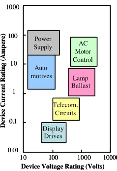
used in motor control, power supplies, and telecommunications. Fig. 1.1 shows a plot of
device current rating versus voltage rating for several solid state power devices
applications [1].
Device Voltage Rating (Volts)
Device
Current
Rating
(Ampere)
10 100 1000 0.01 0.1 1 10 100 1000 Display Drives Telecom. Circuits Lamp Ballast AC Motor Control Auto motives Power Supply 10000
Device Voltage Rating (Volts)
Device
Current
Rating
(Ampere)
10 100 1000 0.01 0.1 1 10 100 1000 Display Drives Telecom. Circuits Lamp Ballast AC Motor Control Auto motives Power Supply 10000
[image:23.612.262.381.509.682.2]Although solid-state power MOSFETs utilize semiconductor processing
techniques that are comparable to those of conventional very large scale integration
(VLSI) circuits, voltage and current levels are much different from the design used in
VLSI devices. While the basic physics of conventional integrated circuit (IC) devices is
applicable, additional concepts need to be considered when high power bipolar junction
transistors (BJTs) and MOSFETs are used in power applications. A high blocking voltage
in the off-state and a high current capacity in the on-state – two characteristics associated
with power devices – usually exceed the limitations of modern conventional transistors to
perform as a high-power switch.
1.2 Advantages, Disadvantages, and Characteristics Comparison with BJT
The driving reason for the invention of the power MOS transistor is the
performance limitations associated with BJTs as a switching device for power
applications. Table 1.1 compares the major characteristics of a power MOSFET to that of
a power BJT [2].
A conventional BJT is a current-driven device. A large amount of base drive
current – as high as one- fifth of the collector current – is needed to keep the BJT device
in the on-state. A fast turn-off response requires a large amount of reverse base drive
current [ 3 ]. Furthermore, BJT devices present a low input impedance characteristic
because they are driven by current from the base-emitter input. In general a complex and
expensive driving circuit is required for the low impedance input, which is a drawback of
a BJT device [4]. In contrast, a MOS transistor is a voltage driven device that produces
low gate leakage currents. Even when high currents are being switched, gate leakage does
not exceed few nano amperes [5]. Since the driving power during switching is small due
to low gate current, the driving circuit is simpler and cheaper compared to that of BJTs
[6]. Fig. 1.2 shows typical driving circuits for both the BJT and MOSFET for a power
switching application. The BJT requires substantial drive circuits to provide forward and
reverse base current, whereas the power MOSFET requires only the application or the
removal of a relatively small amount of charge at turn-on and turn-off [7].
BJTs are described as a minority carrier device in which injected minority carriers
recombine with majority carriers. A disadvantage of this mechanism is that it limits the
device switching speed. Presence of minority carriers makes the switching speed of BJTs
several orders of magnitude slower than a MOS transistor (with no charge-storage
mechanism) of similar size and voltage ratings. Hence, power MOSFET is capable of
higher operating frequencies than BJT [3]. Note that power BJT switching speed is
limited by minority carrier storage, rather than base transit time limitation in high-speed
TTL and ECL logic (a conventional BJT).
A MOS transistor tends to slow down at elevated temperatures. This effect makes
MOS transistor more resistive at increased temperatures and less vulnerable to thermal
runaway effect experienced by BJTs. At high voltage and high current, BJTs suffer from
thermal runaway that leads to a second breakdown. If any local hot spot develops in BJTs,
a larger current will flow at that spot, and further heating of the device happens (because
of the negative temperature coefficient of resistance characteristic of BJT devices). When
a hot spot develops on the BJT structure, all power will concentrate in one spot and local
temperature will be so high that device destruction follows immediately. For a MOS
configuration, if the current in a certain cell begins to increase, the resulting increased
temperature will increase the on-resistance of that cell, thus self- limiting the current.
Devices can be easily configured in parallel since this promotes an even distribution of
current [3, 4].
One of the important device characteristics is its safe operating area (SOA). The
device at which it can be safely used. For a power MOSFET, SOA is defined by the
maximum drain current at 25 ºC, the breakdown voltage (the maximum blocking voltage),
and the maximum power dissipation. In addition to these factors, the second breakdown
effect reduces the SOA of a BJT device. Fig. 1.3 shows SOA of a typical BJT and
MOSFET device. In this figure, the reduction of SOA due to the second breakdown can
be seen [7] for BJT (a dotted line), while MOSFET (a solid line) does not have this effect.
The area of SOA is wider for MOSFET than BJT.
One drawback of a power MOS transistor is its lower voltage and current rating as
compared with BJT due to the MOS transistor’s on-state resistance. Fig. 1.4 shows the
current and voltage limitations of BJT sand MOS transistors. For voltage ratings smaller
than 100 V, MOS and BJT have similar on-state voltage drops. However, at higher
voltage ratings (> 200 V), the on-state voltage drop of MOS becomes higher than that of
a similar size BJT with similar voltage ratings [7]. This simply means that the conduction
loss of a MOSFET is larger than that of a BJT at higher voltage ratings. This fact makes
it more attractive to use BJTs for higher voltage applications at the expense of frequency
response.
1.3 Conventional MOSFET vs. Power MOSFET
For high power applications, a conventional lateral MOSFET structure, shown in
Fig. 1.5, cannot be easily scaled for two main reasons. First, in high power applications, a
wider spacing between drain and source is needed to obtain a high voltage blocking
capability. For the drain junction to have a high blocking voltage, the channel length must
exceed the thickness of the space charge (SC) region on the channel side of the drain
junction to avoid punchthrough. To support the high drain voltage and to avoid
punchthrough, a great amount of valuable surface area of the semiconductor is wasted
using a lateral structure. In addition, having a longer channel will increase channel
resistance and reduce the current rating of the device. Second, in the lateral MOSFET
structure, all connections – source, drain, and gate – are made on the same, upper surface.
This simply complicates the metallization required for each power device. Both effects
consume valuable area, generating a low silicon utilization factor. For these reasons, the
simple lateral MOSFET structures are rarely used as power discrete devices [7].
1.4 Development of Power MOS Devices
For power application, MOS transistors need a reasonable, short channel length
and a low doping level in the drain region. Having a low doping level in the drain will
ensure the space charge layer at the drain-channel junction spreads into the drain regions
instead of the channel region, providing a large blocking voltage capability. In the 1970s,
a unique MOS transistor structure, which avoided two disadvantages of using a
conventional lateral MOS transistor mentioned in 1.3, was developed. This structure,
V-shaped groove MOSFET (VMOSFET), was the first commercially produced power
device. In this structure, the drain contact was formed on the substrate [8]. The current in
this type of structure flows vertically from drain to source. A large current rating can be
achieved by connecting many individual devices in parallel during the metallization
process. Fig. 1.6 shows the cross-sectional view of a VMOSFET [6]. An anisotropic etch
was used to create the V-shaped groove in the semiconductor surface after the p-body
region and n+ diffusion. The channel length of VMOSFET is determined by the depths of
the diffusion that can be controlled down to sub- micrometer range. The most of the
voltage is dropped in the epilayer (n-) region since the epitaxial region is more lightly
doped compare to p-channel region. Each gate of the VMOSFET controls the current
from the two sources (each sides of the groove). This current will flow to the common
drain.
Inherent to a VMOSFET is the current crowding at the tip. This effect can limit
the useful current rating of the device as well as the voltage rating. This problem can be
reduced by using the truncated VMOSFET shown in Fig. 1.7. Although the trench
manufacturing and a high electric field at the tip of the V-groove, therefore the structures
shown in Fig. 1.6 and Fig. 1.7 are replaced by planer designs – lateral diffused MOS
(LDMOS) and VDMOS transistors [3].
Fig. 1.6. The cross-sectional view of a VMOSFET. An anisotropic etch is used to produce a V-shaped groove in the semiconductor surface [6].
A VMOSFET utilizes two successive diffusion steps to define two closely spaced
pn junctions at different depths below the silicon surface. This dual diffusion technique
may be used laterally in the same way. Fig. 1.8 shows the device structure called
LDMOS. The difference between this structure and a conventional lateral MOS transistor
is that the channel length does not depend on the lithography step; rather it depends on
the diffusion processes.
Fig. 1.8. The cross-sectional view of a LDMOS [7].
The commercially successful power MOS design combines the idea of
VMOSFET and LDMOS transistor. This structure is known as the vertical-diffused MOS
(VDMOS) transistor, shown in Fig. 1.9. The VDMOS structure utilizes the dual diffusion
technique to determine the lateral surface channel length (as does LDMOS); however, it
supports the drain voltage vertically in the n- epilayer (as does VMOSFET). The
electrons flow laterally from the source through the channel. The electrons then turn to
Fig. 1.9. The cross-sectional view of a VDMOS [7].
Of the power MOS transistor structures mentioned, the LDMOS and VDMOS are
widely used in high power radio frequency application. VDMOS transistors find
widespread application in broadband low frequency (<1 GHz) applications where they
offer good stability, whereas LDMOS transistors are employed in high frequency and
high gain narrow band applications [ 9]. Again, two major disadvantages of LDMOS
transistors are high series resistance and use of valuable silicon surface real estate [10],
thus making a VDMOS transistor structure a better candidate as a power discrete device
1.5 Thesis Goal and Objective
The sponsor of this work is Spectrum Devices, a company located in Hatfield, PA
that specializes in power devices; especially those waning in production by larger
semiconductor manufacturers. Spectrum Devices is interested in bringing a power MOS
device to market for their customers that meets MRF150 specifications [11]. The goal of
specifications at 50 V operation, and to verify the device performance through transistor
fabrication and characterization.
Documented VDMOS processes were established more than 30 years ago, thus
designs were implemented in process technology common to that period. This project
involved the development of a new process design that takes advantage of modern
process technology, while staying within the capabilities of the SMFL. The objectives of
this work were to (1) verify the new process design that defines the device operation, and
(2) investigate the effects of the Faraday shield (applied for increased breakdown voltage
and increased frequency response) and UIS implant (applied for elimination of parasitic
BJT operation, or avalanche failure) on DC and AC operating characteristics; the theory
behind these implants is covered in Chapter 2. An additional consideration not found in
literature was to ensure that the avalanche-resistant device was a completely self-aligned
structure (source-to-gate), avoiding additional masking levels and ensuring that the
device characteristics are immune to overlay error within the design tolerance.
1.6 Thesis Outline
This thesis is presented over the five remaining chapters. Chapter 2 provides the
theory of the operation of power VDMOS transistors. Chapter 3 describes a power
VDMOS layout design, process recipe development and verification, and details of
process model calibration and device simulation using SUPREM-IV (Silvaco Athena &
Atlas) simulation tools. Chapter 4 provides the fabrication of the VDMOS transistor.
Chapter 5 discusses electrical testing of power VDMOS test structures and test results.
[1] V. Benda, J. Gowar, and D. A. Grant, Power Semiconductor Devices: Theory and
Applications, Chichester: John Wiley & Sons, Inc, 1999.
[2] K. S. Oh, “IGBT Basics 1: Application Note 9016,” Fairchild Semiconductor,
February 2001.
[3] V. Barkhordarian. “Power MOSFET Basics: AN1084,” International Rectifier,
July 2000.
[4] “Understanding Power MOSFETs: Application Note An-7500,” Fairchild
Semiconductor, October1999.
[5] C. G. Jambotkar. “Power Field Effect Transistor.” U.S. Patent 4,145,700, March
20, 1979.
[6] K. S. Oh, “MOSFET Basics: AN9010” Fairchild Semiconductor, July 2000.
[7] D. A. Grant and J. Gowar, Power MOSFET: Theory and Applications, New York:
John Wiley & Sons, Inc, 1989.
[8] Y. Tarui, Y. Hayashi, and T. Sekigawa, “Diffusion self-aligned MOST: A new
approach for high speed devices.” Proc. Conf. Solid State Devices 1, 105-110, 1969.
[9] P. H. Wilson. “A Novel High Voltage RF Vertical MOSFET for High Power
Applications,” IEEE, pg 95-100, 2002.
[10] M. Trivedi and K. Shenai. “Comparison of RF Performance of Vertical and
Lateral DMOSFET,” IEEE, pg 245-8, 1999.
[11] “The RF MOSFET Line. RF Power Field- Effect Transistor: N-Channel
Chapter 2
Theory
2.1 Device Characteristics: Static Operation
Device characteristics of a power VDMOS transistor are much like those of
conventional MOS transistors. In a MOS transistor structure, there are four possible
device types – n-channel enhancement mode, n-channel depletion mode, p-channel
enhancement mode, and p-channel depletion mode. They are shown in Fig. 2.1 with their
circuit symbols and current- voltage (I-V) characteristics. Of these structures, the
n-channel, enhancement mode device is often used for several reasons. Since electrons have
a higher mobility compared to holes, the carrier transit time is shorter for an n-channel
device, giving higher switching speed results and thus reducing the on-state losses [7]. In
an enhancement device, a negligible current normally flows in its normal off state. This
ensures lower power dissipation that compares favorably to a depletion mode device.
The active region of a power VDMOS transistor consists of four distinct regions
between the source region (formed by n+ diffused region) and the substrate region (n+
drain region). This can be seen in Fig. 2.2. In this figure, region A is the surface layer of
the body region. The channel will form at this region at a given gate bias. Region B is the
surface layer of the body region between the source diffusions. Region C is the regions
between body regions. Region D is the drain drift region in the epilayer. Region A
controls the flow of current in the device, whereas any blocking voltages are developed
Fig. 2.1. The four types of MOS transistor operating regions with their circuit symbols and capacitance-voltage (C-V) characteristics [7]. (a) type enhancement mode. (b) n-type depletion mode. (c) p-n-type enhancement mode. (d) p-n-type depletion mode.
[image:37.612.110.535.72.366.2]2.2 Threshold Voltage
A threshold voltage (VT) of a MOS transistor is defined as the gate voltage where
an inversion layer forms at the interface between the insulating layer (oxide) and the
substrate (body) of the transistors. When enough voltage is applied at the gate (VT),
enough electrons accumulate under the gate to cause an inversion layer in Region A of
Fig. 2.2. This forms a conductive channel across Region A. Electrons now flow in either
direction through the channel. As electrons move from the source towards the drain, the
forward positive drain current flows into the source. The process of channel formation
(depletion and inversion) is seen in Fig. 2.3.
[image:38.612.121.532.328.656.2]In a power VDMOS transistor, the main factors controlling VT are gate oxide
thickness (tox) and peak surface concentration (NA) in the channel. The body implant dose
in Region A determines this surface concentration. VT may be increased by using higher
body concentration and/or increasing tox. Fig. 2.4 shows the effect of the body doping
concentration (NA) and interface charge (Qox) on VT. Since the peak body concentration of
VDMOS transistors occurs near the source, VT is determined at the source end of the
channel [7]. In addition, positive charges such as mobile ions in the gate oxide can cause
VT to vary or drift. For this reason, it is necessary to grow the gate oxide layer under
[image:39.612.145.504.332.663.2]extremely clean condition.
Fig. 2.4. The effect of NA and Qox on VT at room temperature [7].
The value of VT is generally measured by making a connection between the gate
and drain. The voltage that must be applied across the devices to achieve a drain current
of 0.25 to 1.0 mA is determined [3, 12]. Typical values of the parameters for a power
VDMOS transistor at room temperature (300K) are as follows [7]:
Body NA = 1 x 1017 cm-3, Source ND = 1 x 1020 cm-3, tox = 100 nm
resulting in an operating threshold voltage ~ 3.5 V. A typical power MOSFET VT are
2 to 4 V for high voltage devices with thicker gate oxides and 1 to 2 V for lower voltage
devices with thinner gate oxides. Further details are provided in Appendix A.
2.3 Typical Output
The typical set of output characteristics (also known as family of curves) for a
power VDMOS transistor is shown in Fig. 2.5. For each curve, gate to source voltage
(VGS) is constant.
A
B
C
In Fig. 2.5, point (A) represents an on-state condition (VGS > VT); this region is
usually known as the ohmic or linear region. Point (B) represents the turn off or blocking
state (VGS < VT); no channel is formed at this region, referred to as cut-off. A negligible
current will flow when sweeping VDS in this region. Point (C), generally known as the
saturation region, represents the constant current region. Saturation describes the
characteristic above the “pinch-off” voltage where a further increase in the drain to
source voltage does not cause any significant increase in drain current [12].
The drain current can be calculated using Equations 2.1 or 2.2 depending on the
region of operation.
(
)
"# $ % & ' ( ( = 2 2 1 Ch Ch T GS
D k V V V V
I (2.1)
(
)
22 1
T GS
Dsat kV V
I = ( (2.2)
where k is known as the device transconductance parameter and calculated using
Equation 2.3 and VCh is the voltage drop along the channel inversion layer, which
excludes the influence of series resistance.
( )
oxn wl C
k =µ (2.3)
where µn is the electron channel mobility, w is the channel width, l is the channel length,
and Cox is the capacitance per unit area of the gate oxide.
2.4 On Resistance
The total on-state resistance of a power VDMOS transistor (RDS(on)) is expressed
as the sum of several different terms: the resistance of the inverted channel (RCH), the
the resistance of the bulk semiconductor – the drain region (RD0), and the resistance of the
substrate (RSub), as shown in Equation 2.4 along with the associated figure.
Sub D
A CH on
DS R R R R
R ( ) = + + 0 + (2.4)
In Fig. 2.6, RD0 is separated further into RJ and RD, where RJ is the spreading
resistance within the space between the p- body regions (also referred to as the JFET
region), and RD is the resistance occurring under the p- body to the top of the substrate.
Rn+, which can be added to the total on-state resistance, is the resistance of the source
region (n+) and is negligible compare to other components that form RDS(on) [1]. The
equations for calculating each resistance value in Equation 2.4 can be found in
Appendix B.
Fig. 2.6. A VDMOS transistor showing its internal resistances (RDS(on)) [6].
Fig. 2.7 shows the relative importance of each of the components to RDS(on) with
different voltage ratings. At higher voltages, RDS(on) is dominated by RD and RJ, since
higher resistivity (low doped) and thickness values in the epilayer are required for higher
avoiding breakdown [4]. At lower voltages, RCH dominates RDS(on). RSub can be ignored in
high voltage MOS transistors; however, it can give a large effect on RDS(on)for voltage
ratings below 50 V.
Fig. 2.7. The relative importance of each of the components to RDS(on) for different
voltage ratings. REPI from this reference is RD0 component in Equation 2.4. Rn+ is
included in Rwcml. Rwcml is sum of bond wire, contact, metallization and lead frame
resistance [3].
The on-state voltage drop and static on-state power loss values can be calculated
using Equations 2.5 and 2.6, respectively.
D on DS
DS R I
V = ( ) (2.5)
2 ) (on D DS
D R I
P = (2.6)
Low RDS(on) values are needed to maintain a low resistive loss associated with the MOS
transistors. Having a lower value of RDS(on) both minimizes the static on-state power loss
of devices and maximizes the current rating of the devices. In addition, minimizing
RDS(on) provides device with superior power-switching performance since the voltage drop
Since the mobility of holes and electrons decreases as temperature increases,
RDS(on) is dependent on the temperature. This effect can be seen in Fig. 2.8. RDS(on)
dependence on the temperature can be estimated by using Equation 2.7, which is given in
reference [6].
Fig. 2.8. Dependence of the junction temperature to RDS(on) [4].
3 2 ) ( ) ( 300 ) ( ) ( to on DS on DS K T Temp Room R T R ) * + , -.
= , (2.7)
where T is the absolute temperature.
2.5 Breakdown Voltage
Breakdown voltage (BVDSS) is the maximum voltage between drain to source that
a MOS transistor can handle without causing avalanche breakdown of the pn junction
formed at the body-drain region in the off-state. There are five driving factors controlling
breakdown: avalanche, reach-through, punch-through, Zener, and dielectric
Avalanche breakdown, the primary breakdown mechanism in power devices, is
caused by the increasing electric field in the depletion region of the body-drain pn
junction up to a critical value. When this critical value is reached, electrons and/or holes
acquire sufficient energy to create electron-hole pairs by colliding with atomic electrons
within the depletion region. Newly created electrons and holes move in opposite
directions due to the electric field, adding more current to the existing reverse-bias
current. In addition, the generated carriers may acquire sufficient energy to ionize other
atoms, leading to the avalanche process [13].
A poorly designed device can have a special case of the avalanche breakdown.
Reach-through breakdown is avalanche breakdown occurring when the depletion region
of the n- epilayer contacts the n+ substrate, whereas punch-through breakdown is
avalanche breakdown occurring when the depletion region of the body-drain pn junction
contacts the n+ source region. Both reach-through and punch-through breakdown occurs
at drain voltages below the rated avalanche voltage of the device [3, 6]. Zener breakdown
occurs typically through a tunneling mechanism in highly doped pn junctions. In a highly
doped junction, the conduction and valence bands on opposite sides of the junction are
sufficiently close enough that electrons may tunnel straight through from the valence
band on the one side (p side) into the conduction band on the another side (n side) during
reverse bias[13].
The pn junction that blocks the voltage in the power MOSFET is structured
between the p- body region and the n- epilayer region (region C and D in Fig. 2.2). In the
supports almost all the blocking voltage (breakdown voltage limit). For this reason, the
maximum theoretical breakdown voltage is dependent of doping profile and thickness of
n- epilayer. To yield a higher breakdown voltage, both the resistivity and the thickness of
the n- epilayer need to be increased [12]. Fig. 2.9 shows the dependence of BVDSS on
doping concentration and thickness for the n- epilayer as described in [14]. BVDSS is
generally measured using VGS = 0 V (shorting of the gate and source) and ID = 250 µA
[3, 6]. Both increasing the epilayer resistivity and thickness increase the value of BVDSS.
Fig. 2.9. BVDSS vs. doping concentration density and thickness of n- epilayer [14].
Fig. 2.10 shows RDS(on) versus BVDSS for some commercially available power
MOS transistors [15]. The value of RDS(on) normally increases with increasing voltage
rating BVDSS, also shown in Equation 2.8. Since it is desired to have low RDS(on) and high
BVDSS values, the tradeoff makes it a difficult task to specify the optimum doping and
Fig. 2.10. BVDSS vs. RD(on) for commercially available power MOS transistors, showing
the design tradeoff [15].
6 . 2 )
(on VDSS
DS B
R / (2.8)
Although the breakdown voltage of a VDMOS structure is controlled by the
doping concentration and the thickness of epilayer, it is also controlled by the junction
shape and the structure of the region where the junction meets the semiconductor surface.
This is due to the altering of an electric field at the periphery of junctions; the electric
field is typically increased locally, and the breakdown voltage of a device will be
decreased. To obtain a higher breakdown voltage, either the radius of the junction needs
to be altered or the space charge region at the semiconductor surface needs to be widened
to decrease electric field at the space charge region [1]. This is achieved in three different
ways: (1) using a guard ring structure (diffusing extra floating regions around the
circumference of junctions) [5], (2) implanting a lightly doped layer around the perimeter
of the pn junction, and (3) using a field plate [12]. Out of these options, the VDMOS
structure fabricated in this work implements the guard ring approach to increase the
breakdown voltage of a device. To see the effect of a guard ring structure on BVDSS values,
several different ring structures – single ring and double ring – were created on a mask
2.6 Transconductance
The forward transconductance (gfs) of the MOS transistor is an important on-state
parameter that tells the sensitivity of ID to changes in the VGS. If gfs is high enough, high
current handling capability can be obtained from a low gate driving voltage [7]. The
value of gfs for linear and saturation regimes are defined in Equation 2.9. gfs is extracted
for a VDS that guarantees operation in the stable constant current region and for a VGS
which gives ID approximately one half of the maximum current rating value. For
comparison reasons, gfs is extracted when ID is 5 A and VDS is at 10 V.
Ch ox n V GS D
fs C V
l w V I g DS µ = " # $ % & ' 0 0
= (Linear region)
(
GS T)
ox n V
GS D
fs C V V
l w V I g DS ( = " # $ % & ' 0 0
= µ (Saturation region) (2.9)
As shown in Equation 2.9, the value of gfs can be controlled easily by varying the
gate width (w), the channel length (l), and the gate oxide thickness (tox) of the transistor.
Decreasing tox, decreasing l, and increasing w increases gfs. Decreased l value, therefore,
is beneficial to both gfs and RDS(on). In the VDMOS structure fabricated in this work, an
interdigitated layout was used to enhance w. The channel length (l) was precisely
controlled by multiple diffusion steps, which were verified by the ATHENA simulation
software.
Having a higher gfs value increases both maximum operating frequency and
2.7 VDMOS: Capacitive Elements & Dynamic Behavior
The high frequency performance of a power MOS transistor is determined by the
time required to establish voltage changes across capacitances. For this reason,
understanding of the internal capacitance of a power MOS transistor, as shown in Fig.
2.11, is crucial. The capacitances include: Cgs (the capacitance between gate electrodes to
the source region; independent of applied voltage), Cds (the capacitance between the n+
drain to source region; varies inversely with the square root of VDS), and Cgd (the
capacitance between the gate electrodes to the n+ drain region; a nonlinear function of
voltage due to change in n- depletion). The values of capacitances are determined by the
structure of the MOS transistor, materials involved, and by the voltages across them [3,
7]. Detailed equations to calculate internal capacitance values can be found in Appendix
B-2.
Since data sheets typically give terminal capacitance specifications rather than
each internal capacitance value, it is necessary to relate terminal capacitances to internal
capacitance values. The three capacitances generally used in data sheets are the input
capacitance (Ciss), the output capacitance (Coss), and the reverse transfer (or Miller)
capacitance (Crss). These capacitances can be related to the physical capacitances and
relationships as shown in Equations 2.10, 2.11, and 2.12. Ciss is the parallel combination
of Cgd and Cgs. Coss is the parallel combination of Cds and Cgd. Crss is same as Cgd.
gs gd
iss C C
C = + (2.10)
gd ds
oss C C
C = + (2.11)
gd
rss C
Coss (with a typical value of ~250 pF) is mainly a junction capacitance of a diode
formed between the p- body region and the n epilayer. This capacitance value is highest
when no bias is applied across drain to source/body. When the drain voltage is increased,
the depletion width increases. Since the capacitance is inversely proportional to its plate
spacing, it decreases rapidly with increasing depletion width.
Ciss (with a typical value of ~400 pF) does not vary with a change in drain to
source/body bias. This capacitance is mostly formed between source metal interconnects
to gate material. To maintain a low input capacitance value, the oxide thickness can be
increased. Although small in value, gate to source overlap capacitance and gate to
channel capacitance also contribute to Ciss [16].
Although Crss (with a typical value of ~40 pF) has the lowest capacitance value
among the three capacitances, it has the most effect on RF performance. Crss provides a
negative feedback loop between the output and the input of the circuit, which can
theoretically roll off the frequency response rapidly.
The maximum operating frequency of power MOS transistors can be found using
Equation 2.13.
(
ton toff)
f+
1 "
1
max (2.13)
where ton is the overall turn-on time and toff is the overall turn-off time [1]. The equations
to obtain ton and toff are in Appendix C.
Ciss must be charged to the threshold voltage before the device begins to turn on
and discharged to the certain voltage before the device turns off. For this reason, Ciss has
a direct effect on the turn-on and turn-off time of the device. Looking at the relationship
shown in Equations 2.13 and C.1 to C.6, if Cgs and Cgd can be reduced, it is possible to
work in the high frequency regime. The maximum operating frequency also is dependant
of transconductance value mentioned in section 2.6 [16]. It is shown that fmax is directly
proportional to gfs and inversely proportional to Ciss, shown in Equation 2.14.
iss fs C
g
fmax / (2.14)
The gate bonding pad and the entire metal layer connected over the field oxide
result in a substantial capacitance from the pad to the drain substrate. For this reason, a
lightly doped diffusion (p-) can be placed under the pad. This diffusion layer is connected
to the source region and acts as a conductor between the gate pad and the drain substrate,
reducing the effect of Cgd. The implant done for this method is called the Faraday shield
implant and is used in the VDMOS device to shift the parasitic gate-field capacitance
Fig. 2.12 (a) and (b) show the cross-sectional view of a VDMOS with and without the
Faraday shield implant.
The Faraday shield implant is also used to enhance the breakdown voltage of the
VDMOS device. It was mentioned in section 2.5 that a higher breakdown voltage of a
VDMOS device can be achieved by using a diffused field- limiting guard ring structure.
That is to use an extra floating diffused regions around the circumference of (body-drain)
pn junction. By having this structure, the width of the space charge region at the junction
is widened, thus decreasing the electric field formed in the space charge region, with the
result that the junction breakdown voltage is decreased.
(a)
(b)
2.8 VDMOS Parasitic BJT
A power MOS transistor has a parasitic BJT as an inherent part of its structure.
The parasitic BJT can be seen in both VMOSFET and VDMOS structures. Fig. 1.9 shows
the cross-section of VDMOS with a parasitic BJT. The n+ source terminal corresponds to
the n-type emitter, the p- body region corresponds to the p-type base, and the n-type drain
corresponds to the n-type collector. Also shown in Fig. 2.13 is the lateral resistance in p-
body region from the contact to the shoulder (Rbb’).
Fig. 2.13. The cross-section of a power VDMOS showing a parasitic BJT [7].
If the parasitic BJT turns on, it will completely short-circuit the MOS transistor.
conditions this is suppressed by shorting the source (emitter) and body (base) regions,
and thus preventing the device from ever establishing an emitter-base voltage [7].
However, the parasitic BJT can be initiated during high-speed switching of the
MOS transistor. In circuits with an inductive load, the rate of the rise of the VDS can be
very high. When the VDS rate of increase is large at turn off state of high-speed switching,
there is a voltage drop between the drain and the source region. This voltage drop creates
a displacement current through Cbd (the capacitance between the base of the BJT and the
drain of the MOSFET) resulting from the capacitive charge and discharge. The induced
current now transfers to Rbb’. If the voltage drop across Rbb’ exceeds about 0.6 V, it is
sufficient to forward bias the base-emitter junction of BJT, and turn on the parasitic BJT
[7]. Under this condition, the breakdown voltage of the MOSFET is restricted to that of
the open base breakdown voltage of the BJT. If the applied VDS is higher than the open
base breakdown voltage of BJT, then the MOSFET will enter the avalanche stage and
may be destroyed if the current is not limited externally [3].
The method to reduce the parasitic BJT without changing the characteristics of a
power VDMOS transistor is implanting an additional higher doping diffusion in the p-
region [6]. This higher doped region significantly reduces the Rbb’ value (thus the voltage
drop necessary to forward bias the parasitic BJT occurs at higher current and
temperature), while increasing the doping in the parasitic base and eliminating the current
gain mechanism. This extra doping is implanted following the body doping process [17].
It is important to ensure this extra implant step has no effect on other characteristics of a
significantly affect the VT of the device. In the proposed structure this extra implant step
is termed the UIS implant, named after the high- frequency testing procedure (Unclamped
Inductive Switching) which is used to verify the VDMOS operation and resistance
against this parasitic effect. In addition, the cell and line layout can be optimized to
minimize the length of Rbb’, thus reducing Rbb’ value.
2.9 Conventional VDMOS Process Flow [7]
The fabrication steps for a conventional power VDMOS transistor (shown
previously in Fig. 1.9) include several deposition, implantation, lithography, and
diffusion sequences, which are comparable to conventional MOS transistor fabrication. In
this section, typical fabrication steps of an n-channel VDMOS device are shown. More
thorough process steps can be found in chapter 5.1 of the reference [7].
A standard n-channel VDMOS transistor is fabricated on an n-type (100) oriented
wafer. The thickness of the wafer is selected within the range of 250 to 500 µm. If the
substrate is too thick, the thermal resistance of the final device is greater. This is not
suitable since heat dissipated in the device has to be removed through the full thickness
of the substrate. If the substrate is too thin, breakage might occur during the fabrication.
The substrate thickness adds to RDS(on) of the transistor; especially in low voltage devices.
A typical value of the phosphorus doping concentration of a substrate is 1x1018 cm-3. This
high doping concentration ensures resistivity of the substrate to be low. (~ 0.02 O-cm).
An RCA clean (after Radio Corporation of America) is done prior to the n-type
the intended voltage rating of the transistors. The epilayer thickness of 20 µm (1 O-cm)
for 50 V devices and of 50 µm (20 O-cm) for 500 V devices are used.
The surface of the epilayer is first oxidized for masking process. This masking
process defines the p+ well, which connects the channel regions back to the source
contact. Windows are etched through the oxide layer, with 1x1014 cm-2 boron atoms
implanted at low energy. This implanted area is diffused with a drive- in process to form a
pn junction with depth of ~ 5 µm. The second masking process is done using the same
oxide layer. This process uses the reverse of the first masking process. This time around,
all oxide except where the p+ wells are formed is etched with Hydrofluoric Acid (HF). A
high energy implant of phosphorus (100 keV with 1x10-12 to 1x 10-13 cm-3) is then
performed to ensure a higher conductivity under the gate oxide (illustrated in Fig.
2.14(a)). After another RCA cleaning step is done, the gate oxide (50-100 nm) is grown
and a polysilicon gate (0.5 µm) is deposited. The polysilicon gate is then doped heavily
with phosphorus.
A
![Fig. 1.9. The cross-sectional view of a VDMOS [7].](https://thumb-us.123doks.com/thumbv2/123dok_us/59970.5586/33.612.164.482.71.320/fig-cross-sectional-view-vdmos.webp)
![Fig. 2.1. The four types of MOS transistor operating regions with their circuit symbols and capacitance-voltage (C-V) characteristics [7]](https://thumb-us.123doks.com/thumbv2/123dok_us/59970.5586/37.612.110.535.72.366/transistor-operating-regions-circuit-symbols-capacitance-voltage-characteristics.webp)
![Fig. 2.3. The process of a channel formation. (a) and (b) shows the depletion region formation, whereas (c) shows the formation of the inversion layer [6]](https://thumb-us.123doks.com/thumbv2/123dok_us/59970.5586/38.612.121.532.328.656/process-channel-formation-depletion-region-formation-formation-inversion.webp)
![Fig. 2.4. The effect of NA and Qox on VT at room temperature [7].](https://thumb-us.123doks.com/thumbv2/123dok_us/59970.5586/39.612.145.504.332.663/fig-effect-na-qox-vt-room-temperature.webp)