Md Shakil Ahmed and Ivan Glesk
1
Department of Electrical and Electronic Engineering, University of Strathclyde Royal College Building, 204 George Street, Glasgow G1 1XW, United Kingdom
Received 5 June 2015, accepted 8 June 2015
It is important to understand properties of different materials and the impact they have on devices used in communication networks. This paper is an overview of optical non-linearities in Silicon and Gallium Nitride and how these nonnon-linearities can be used in the realization of optical ultra-fast devices targeting the next generation integrated optics. Research results related to optical lasing, optical switching, data modulation, optical signal amplification and photo-detection using Gallium Nitride devices based on waveguides are examined. Attention is also paid to hybrid and monolithic integration approaches towards the development of advanced photonic chips.
PACS: 42.79.Sz, 42.82.Gw, 85.60.Bt, 42.70.Nq
Optical Nonlinearity, Broadband Communications, Optical Waveguides,
KEYWORDS: Photonic Chips, All-optical Switching, GaN Platform, Refractive Index, CMOS Compatibility, Hybrid Integrated Platform, Nonlinear Effects
Contents
1 Introduction 67
2 Optical Nonlinearity Overview 68
2.1 First Order Nonlinearity………... 69
2.2 Second Order Nonlinearity……….. 70
2.2.1 Linear Electro-optic Effect (LEO)………. 72
2.2.2 Second Harmonic Generation in Waveguides………... 73
2.2.3 Optical Nonlinearity in Optically Active Medium - SOA and TOAD….. 74
2.3 Third Order Nonlinearity………. 75
2.3.1 Applications of Third Order Optical Nonlinearity……… 78
2.4 Silicon Photonics Limitations and The Emergence of GaN Photonics……… 80
. . 1 E-mail address: ivan.glesk@strath.ac.uk
3 Towards CMOS Compatible GaN Photonics for Broadband Communication 82
3.1 CMOS Compatibility Issues and GaN Photonics……… 82
3.2 Fabrication of GaN Waveguides on Silicon……… 84
3.3 Optical Properties of GaN Waveguide……… 85
4 GaN Passive Waveguide Devices for Broadband Communication 86
4.1 Waveguide Basics……… 86
4.2 Exploitation of Material Refractive Index in GaN Waveguides……….. 87
4.2.1 Birefringence of GaN Waveguide………. 91
4.2.2 Carrier-induced Index Change in GaN Waveguide……….. 91
4.3 AWG for Multiplexing and De-multiplexing using GaN/AlGaN Hetero-structures……….. 93
4.4 GaN Bragg Reflection Waveguides………. 94
4.5 GaN Photonic Crystal Waveguides……….. 95
4.6 GaN Nanowires as Waveguides……… 96
5 GaN Active Waveguide Devices for Broadband Communication 99
5.1 GaN Waveguides with Quantum Wells and Characteristics……….. 99
5.2 Optical Nonlinearity in GaN/AlGaN Quantum Wells……… 101
5.3 GaN Waveguide Switches and Modulators……… 102
5.3.1 GaN/AlN Electro-absorption Modulators……… 105
5.3.2 GaN/AlN Electro-Optic Modulators………. 108
5.4 Lasing in GaN Nanowires………109
6 Overview of Selected GaN Based Devices for Broadband Communication 114 6.1 GaN Photodetector……….. 114
6.2 GaN Optical Amplifier……… 118
6.3 GaN VCSEL……… 123
7 Hybrid Integrated Platform Towards Photonic Chips for Broadband Communication 126 7.1 Use of Ga and Its Alloys for Lasing on Si……….. 126
7.1.1 Hybrid Lasers……… 127
7.1.2 Monolithic Optoelectronics Integrated Circuits (OEIC) on Si………. 128
7.2 Use of Hybrid Waveguides for Photonic Integrated Chips……… 130
7.2.1 Lithium Niobate Waveguide Devices as LNOI……… 132
7.2.2 Lithium Niobate Microrings Using Gallium Nitride Waveguides………… 134
1 Introduction
The use of photons instead of electrons is the main motivation for a development of future photonic devices which will be faster and consume less power to operate. But the question is, ‘How to achieve it and how far away we are from this goal?’ First of all, continuing the present efforts of making faster electronics will still go on, thanks to the support of the multi-billion dollars well established industry. The difficulty we are facing is that the silicon (Si) is running out of ‘steam’ [1,2] and already imposes bandwidth limitations on electronics, electronic devices and copper-based interconnects in broadband communications. It is therefore essential to replace copper-based interconnects with a fibre optic solution. At this stage very limited numbers of currently available optoelectronic devices are used in places, where both the optical and electronic domains meet in order to achieve the best possible performance. But here again, the limitation is the need for controlling these optoelectronic devices by the bandwidth limited electronics. The only way to change this is to develop all-optical chips and devices, where only light signal is used to control light carrying data.
It has been possible today to transmit and receive multi Tb/s of aggregate data throughputs over a single optical fibre, but is it possible to do the similar at a much smaller scale when using optical waveguides? Here, Si will be used as the waveguide core supported by the cladding layer made of a lower refractive index material of SiO2 for confinement. This approach is
known as Silicon on Insulator (SOI). Due to the high contrast in the refractive indices of the core and cladding layers, the waveguide is used as an effective light guiding medium and the manipulation of light via optical nonlinearity is possible to achieve. The goal is to develop “waveguide-based devices” to perform functions like all-optical switching, wavelength conversion, data detection and amplification in the optical domain. Other desired functions such as optical lasing and direct intensity and phase modulations are difficult to achieve by using only Si photonics, mainly due to its centrosymmetric crystal structure and narrow band-gap properties [3]. Therefore exploring other semiconductor material platforms such as GaN photonics were considered. Importantly, GaN is also CMOS compatible.
The principal objective of this paper is to explore how far the GaN platform can be taken to underpin the all-optical devices for photonic chips fabrication for their use in broadband optical communications.
2 Optical Nonlinearity Overview
Si offers optical nonlinearity, exploiting of which is possible to go beyond the switching speed of 100 Gb/s [4]. Moreover, Si is CMOS compatible. Lasers, data modulators, amplifiers, detectors are among the main building blocks for enabling fibre optics communications and signal processing in networks. However some obstacles are found in achieving these goals. First, the minimum band gap of Si does not suit optical emission, second, the centro-symmetric crystal structure of Si impedes the electro-optics modulation and third, due to high frequency generation there are fast and slow free carrier emissions which reduce the performance. But, in course of gradual improvement in technology and nano-fabrication, it is possible to overcome these problems to some extent. In this section, the mathematical derivation of optical nonlinearity is discussed and how exploiting this nonlinearity, especially its third order, can be exploited by using different means to achieve some of our goals.
In 1961, Franklin found a weak optical signal of 347.1 nm in a quartz material when influenced by a light intensity of 694.2 nm by a ruby laser [5]. Franklin deduced that, the result was due to interaction of two optical electric fields in the quartz material producing the second harmonic response. Within a year of Franklin’s discovery of second harmonic generation measurements, a good number of works were carried out in formulating the probes (in the scientific fields) basing on the nonlinear concept. In fact, optical nonlinearity is a phenomenon of the optical electric field induced modification in the properties of the material. The term nonlinear means that the optically induced changes in the material depend on more than one optical field strength in the region. Normally a single source with very high optical intensity like a laser source is sufficient to produce perturbation in the optical properties of the material. This process is quite different from the conventional or linear response of the optical signal, where the changes in the reflection, propagation and absorption depend linearly with the intensity of the optical source. In other words, optical nonlinearity is nothing but the interaction of the electric field of the incident photon with the electrons of the outer shells of the medium induced electric field. As a result, some peculiar phenomenon happens, such as:
a. phase change of the incident signal
b. generation of a new frequency
c. all-optical control of light
The mathematical relation between the induced polarization (P(t)) and the electric field (E(t)) in an isotropic medium having instantaneous dielectric response can be expressed as [6]:
P(t) = ε0(χ(1)E(t) + χ(2)E2(t) + χ(3)E3(t) + …). (2.1)
Here, χ(1) represents the first order susceptibility, χ(2) represents the second order susceptibility
and χ(3) represents the third order susceptibility. In case of centro-symmetric material and in its
2.1 First Order Nonlinearity
χ(1) is the 1st order susceptibility which deals with dipole excitation with bound and free electrons
induced by a photon. The susceptibility term χ(1) is having two parts, one is real part which is
associated with the refractive index and the other one is imaginary part which is associated with loss or gain. To understand the contribution of bound electrons to the susceptibility, the following equation developed by Lorentz may be presented [4]:
χ(1)Lorentz = 𝜔!! / (𝜔!! – ω2 + 𝑖 𝛾!ω). (2.2)
Here, it is shown that the refractive index changes strongly near a resonance. This model provides the susceptibility of bound states belonging to a density of N dipoles. In the above equation, 𝛾!is the damping constant, ω0 is the resonance frequency of the bound state, 𝜔! is the Lorentz plasma frequency defined as 𝜔!! = Nq2/(ε0me), where, q = elementary charge, ε0 =
permittivity of vacuum, and me = effective mass of dipoles. The other factor of susceptibility is
free carriers, which absorb photons and has an effect on the refractive index. The susceptibility which is related to free carriers is defined as the following expression known as Drude model which was mainly derived from equation 2.2 by dropping the restoring force, i.e., 𝜔!=0:
χ(1)Drude = 𝜔!! / (–ω2 + 𝑖 𝛾!ω). (2.3)
Here, the plasma frequency 𝜔! is defined as 𝜔!! = Nq2/(ε0me). The plasma frequency 𝜔! and
damping constant 𝛾! have different values than the corresponding values 𝜔! and 𝛾!of equation 2.2. Any kind of contribution from either bound state or free electron oscillations contributes to the complex refractive index. To sum up, the refractive index may be defined as of the following expression:
n2 = 1 + χ(1)
Lorentz + χ(1)Drude . (2.4)
This refractive index n, changes with both wavelength and carrier concentration N. There is also a useful function for the refractive index ‘n’ as a function of wavelength λ, Ne and Nh. Where, Ne
is the electrons concentration and Nh is the holes concentration of free-carrier contributions to the
refractive index. The function is shown as:
Here, n0(λ) is wavelength dependence of refractive index, ∆nf is the free carrier index change
known as FCI and ∆αf is the free carrier absorption change known as FCA. For Si, n0(λ) is
related to Sellmeier equation:
𝑛!!(λ) = ε + !!! +
!!!!
!!!!!! . (2.6)
This equation also describes the material dispersion of Si. From the equation, it was also known that the closer the photon gets to Si band-gap energy (1.12 eV), the stronger will be the refractive index changes. A good knowledge on material dispersion and engineering the waveguide dispersion is important for efficient conversion of higher order nonlinear terms [7]. FCA produces time-dependent fluctuations of refractive index and subsequent losses in Si which translates to distortions limiting the uses of Si at low operation speeds [8].
2.2 Second Order Nonlinearity
The symmetry of GaN crystal structure is having the presence of intrinsic second order nonlinearity which is known since 1960s (Philips and Van Vechten [9], Levine [10]). In the equation (2.1), the first term represents the first order optical nonlinearity, where the susceptibility phenomena depend linearly on the amplitude of incident optical field. The other terms χ(2) and χ(3) represent the second and third order susceptibilities describing induced polarizations exhibiting quadratic and cubic field dependencies. However, optical nonlinear effects that are commonly seen are listed in Table 2.1 [11] where the terms in bold represent the phenomena those have been seen and predicted theoretically in GaN.
Table 2.1: Various Second and Third Order Nonlinear Optical Phenomena
Second Order Phenomena Third Order Phenomena
Sum-frequency Generation Stimulated Raman Scattering
Difference-frequency Generation Optical-field induced Birefringence
Second Harmonic Generation Two-photon Absorption
Parametric Amplification Self-focusing
Optical Rectification Phase Conjugation
Optical Field-induced Magnetization Third-harmonic Generation
Linear Electro-optic Effect (LEO) Electric-field induced SHG
To model the second-order optical response, let us consider the expression for the time dependent incident field having more than one frequency components as [11]:
E(t) = ! (En 𝑒!!!!! + c.c.). (2.7)
Here, the summation extends from the positive and negative frequencies of individual field components and c.c. is the conjugate of the complex field amplitude. In the second order process, the incident field is composed of two distinct frequency components ω1 and ω2 resulting an
incident field given by:
E(t) = E1𝑒!!!!! + E2𝑒!!!!! + c.c. (2.8)
Now substituting equation (2.8) into the second order term in equation (2.1) generates a nonlinear polarization source having many distinct frequency components due to the various couplings between the ω1 and ω2 fields:
P(2)(2ω
1) = χ(2)(2ω1; ω1, ω1) E12,
P(2)(2ω
2) = χ(2)(2ω2; ω2, ω2) E22,
P(2)(ω
1 + ω2) = 2χ(2)(ω1 + ω2; ω1, ω2) E1E2,
P(2)(ω
1 - ω2) = 2χ(2)(ω1 - ω2; ω1, -ω2) E1E2*,
P(2)(0) = 2χ(2)(0; ω
1, -ω1) E1E1* + 2χ(2)(0; ω2, -ω2) E2E2*. (2.9)
The terms above represent second harmonic generation (2ω1, 2ω2), sum-frequency generation
(ω1 + ω2), difference frequency generation (ω1 - ω2) and optical rectification (0) respectively.
Each term acts as a source for new electric field which oscillates at the frequency of respective nonlinear polarization. According to Shen [12] and Yariv [13], the electric field and polarization terms in equations (2.1) and (2.7) to (2.9) are written as scalars but in general they are vector quantities. The effect of second order nonlinearity is represented by the nonlinearity susceptibility tensor χ(2) as it describes the coupling interaction between the electric fields ω1 and ω2 and the material of interest. The independent tensor elements of the hexagonal GaN crystal
are χ(2)
xzx, χ(2)zxx, χ(2)xxz and χ(2)zzz which are non-vanishing in nature (According to Boyd [14],
Shen [12], Levenson and Kano [15]). Sometimes, the second order nonlinearity coefficient is represented as:
d!"# = χ!"#
(!)
/ 2. (2.10)
It is important to know the concept of the Linear Electro-optic Effect, as it will be instrumental in understanding the GaN Electro-optic Modulators.
2.2.1 Linear Electro-optic Effect (LEO)
The electro-optic effect, which is a second order nonlinearity, occurs with the non-centrosymmetric materials only. In this case, the nonlinear response occurs from a dc electric field induced variation in the refractive index of a nonlinear material which produces a corresponding phase or intensity variation of an optical field that is transmitted through or reflected from the electrified sample [11]. The nonlinear response of LEO effect (magnitude) is also dependent linearly on the applied electric field which can be expressed by the following equation (Boyd [14]):
P(2)(ω) = χ(2)(ω : ω, 0) E(ω) E
dc . (2.11)
Here, E(ω) is the optical field, Edc is the dc electric field. There is an advantage of using
electro-optic effect compared to frequency conversion. The phase matching condition between the fundamental and generated fields is not required because of identical frequencies of the two optical waves. Because the electro-optical effect is the nonlinear field induced change in the refractive index, this nonlinear effect is more conveniently expressed as [11]:
Δ(!
!!)!" = !𝑟!"#𝐸!. (2.12)
Here, Δ(!!!)!" is the ij-th component of the variation of inverse refractive index, 𝐸! is k-th component of the dc electric field and 𝑟!"#which is the electro-optic tensor,is related to χ!"#
(!) as per the following expression [11]:
𝑟!"# = ! !!"# (!)
!! . (2.13)
The above equation depicts that, electro-optic coefficient 𝑟!"# has the same symmetry condition
as that of χ(2), which in turn indicates that it vanishes in centrosymmetric materials. The
expression also confirms that the non-vanishing elements of these two terms χ!"#(!) and 𝑟!"# are
Fig. 2.1: Structure of an optical thin-film waveguide. The refractive indices of the three layers are n0, n1 and
n2, with n1 > n0, n2.
2.2.2 Second Harmonic Generation in Waveguides
There are a good number of advantages in having optical nonlinearity based in waveguides [16]. First of all, a laser beam can be focused into an optical waveguide where it remains trapped over a long distance, whereas, in a bulk material, the focused beam readily diffracts from the focal point. Secondly, the phase matching in a waveguide is obtained by changing the waveguide structure which also determines the propagation characteristics of the waves. Thirdly, besides the phase matching, the nonlinear interactions of the wave can also be varied by varying the waveguide structure. Here, second-harmonic generation is used to explain the last two points. To understand this, let us go through a thin film waveguide as shown in the Fig. 2.1 [16].
For monochromatic waveguide propagation mode, we have the following expression from the theory of dielectric waveguides [16]:
E = ξ(x,y) exp[iβz – iωt]. (2.14)
ξ(x,y) and β(ω) depend on the mode order, waveguide structure (waveguide width W, refractive indices n0, n1 and n2 of three sections as shown in Fig. 2.1) and polarizations (TE or TM). For
presence of both fundamental and second-harmonic waves in the guided mode, the phase matching condition is satisfied when,
2β(ω) = β(2ω). (2.15)
For a given ω, the above equation can be satisfied by adjusting either W or one of n’s. The nonlinear polarization at 2ω is also responsible for the second harmonic generation. The second harmonic generation is expected to be concentrated in those regions of the waveguide, where there is no inversion centre in the materials and |ξ(x,y,ω)|2 is strong. This has evolved into a
Fig. 2.2: Schematic diagram of TOAD.
the width W should be constant, or else, it will not satisfy the phase matching condition of equation (2.15) in the entire waveguide. Secondly, the surface imperfection greatly enhances the loss that is why the propagation length is limited to a few mm in a waveguide. Another reason is that, the high power laser may at times damage the waveguides. Many other nonlinear effects on the waveguides are yet to be investigated. However, the progress would depend on the rapid advances in the development of photonic waveguide technology [16]. Examples of more Second Harmonic Generation and Parametric Amplification using GaN Bragg Reflection Waveguides are discussed in Chapter 4.
2.2.3 Optical Nonlinearity in Optically Active Medium - SOA and TOAD
Semiconductor Optical Amplifier, SOA represents an active optical medium for generating optically induced nonlinearity [17]. SOA based devices now-a-days, show a great possibility of integrating with other photonic components and are used as building blocks for the development of all-optical switches, de-multiplexers, wave length converters, dispersion compensators and photonic memories [18]. One important application of SOAs is in ultrafast all optical switching in the device known as Terahertz Optical Asymmetric De-multiplexer (TOAD) [17]. The TOAD’s switching window width is determined by the SOA offset from the central position of the loop. Here, the data input through a 50:50 coupler is split into CW and CCW components. The CW pulse will reach the SOA later than CCW pulse for the asymmetric position of SOA in the loop and the delay is represented by 2∆xSOA /cfiber. Here, ∆xSOA is the offset of the SOA
position from the centre of the fibre loop and cfiber is the speed of light. In the absence of any
control signal, the CW and CCW pulses propagating within the loop will experience the same unsaturated gain and then recombine at the input coupler and will emerge from the reflected port. The introduction of a control pulse through the second coupler in CW direction (see Fig.
experience different gain saturation profiles (indices of refraction) and after the interference the data will exit from the output port as soon as they recombine at the input coupler, thus producing the switching effect. An important advantage of TOAD as a switching device is that it is not affected by temperature variations and data output stabilization is not required because the data experience the same medium of propagation [17] within the loop. The TOAD has been demonstrated as an ultrafast all optical demultiplexer, routing switch in 250 Gb/ OTDM data network [19, 20], all optical binary flip-flop circuit [21] and in other ultrafast all optical signal processing applications [22, 23, 24, 25, 26].
2.3 Third Order Nonlinearity
The third order susceptibility is important for Si photonics as it shows a good number of phenomena suitable for switching. This can be understood for an electric field E comprising three frequency components ωk:
E(r,t) = !!!!𝐸! = !! !!!! (𝐸!!!(r,ωk) 𝑒!!!! + c.c.) (2.16)
Here, c.c. denotes the complex conjugate. Now substituting equation (2.16) into equation (2.1) and expanding the frequency components of the third order nonlinear term, a multitude of terms can be obtained at new frequencies for third order polarization:
P(3) = !
!ɛ0 χ
(3) [𝐸
!!
!
𝐸!+ ::] + !!ɛ0 χ(3) [(𝐸!!
!
+ 𝐸!! !
)𝐸!+ ::] + !!ɛ0 χ(3) [(𝐸!!!𝑒!!!!+c.c.) + ::] +
!
!ɛ0 χ
(3) [ !
! (𝐸!!!𝐸!!𝑒!(!!!!!!)!+ c.c. ) + ::] + …. (2.17)
Here, each term refers to a particular third order nonlinear process. :: denotes all permutations of possible frequencies. Each term also corresponds to a nonlinear optical excitation. According to the energy level diagram, depicted in Fig. 2.3, it is seen how 3 photons induce dipole transitions to excitation states and then relax back by releasing a fourth photon. The relaxation process takes place instantaneously if the excited state does not correspond to the bound eigenstates of the cry-stal. Out of many such nonlinear processes, those maintain energy and momentum conservation
FWM
Fig. 2.3: Illustration of a dipole excitation and possible energy level diagrams.
known as phase-matching, produce efficient excitation. By choosing the energy levels and phase matching appropriately, a particular non-linear process can be selected to some degree. The first term in the above expression corresponds to a phenomenon known as self-phase modulation (SPM). This results from dipole excitations induced by three photons, as depicted in Fig. 2.3. Intensity dependent refractive index change n2 happens due to SPM. This change in turn alters
the spectral composition of the same pulse which has generated it. As a result, pulse broadening takes place and due to extreme level of SPM, there is a possibility of super-continuum generation. SPM generating photons can also excite to an energetically higher state, as shown in the two photon absorption (TPA) diagram of Fig. 2.3. TPA excitations correspond energetically to an excitation of an electron in the valance band to the conduction band and as such they are ‘absorbing’. It leads to an intensity dependent contribution α2 to the linear absorption coefficient α0. Free carriers in the conduction band, which is the origin of FCA and FCI changes, are
generated by TPA. Hence, the speed of the Si photonic devices slows down due to long lasting processes of FCA and FCI for long lifetime of the free carriers in the conduction band. Changes due to intensity dependent refractive index and the absorption associated with SPM and TPA affect the complex refractive index n by the following relationship [4]:
n = n0 + n2I – i!!! (α0 + α2I) . (2.18)
Here, n2 is the Kerr coefficient, I is the intensity and α2 is the TPA coefficient which are all
related to the real and complex terms of the third-order susceptibility expressed as [4]:
𝑛! = ( !
!!!!!!)
!
!Re ( χ
(3) ),
𝛼! = (– !
!!!!!!)
!
! Im ( χ
(3) ).
(2.20)
There is an important term called as FOM used to compare the Kerr coefficient (n2) with the
strength of TPA coefficient α2 [4, 27]:
FOM = (!
!) (
!!
!!). (2.21)
Higher FOM is desirable to avoid TPA related speed limitation. Si has very high Kerr coefficient n2 = (4.5 ± 1.5) × 10-18 m2 W-1 at 1.55 µm, but the large TPA coefficient α2 results in
very low FOM of 0.4. Hence, the goal is to get the appropriate material with very high Kerr coefficient and low TPA coefficient α2, so that FOM becomes high. The parameters n2 and α2
vary with the changes of wavelength. The Kerr coefficient in Si has maximum value in the range of 1.8 µm to 1.9 µm whereas beyond 2 µm, the TPA coefficient decreases significantly. As such, Si shows very good Kerr nonlinearity with considerable large amount of FOM in the near-infrared region.
Third Order Nonlinearity in Photonic Waveguides: To exploit the optical nonlinearity, special types of waveguides are used. The general guidelines for designing the waveguides supporting strong nonlinear interactions are mentioned as follows [4]:
a. the high optical field confinement should be provided by the waveguide b. the waveguide material should have high Kerr coefficient
c. FOM should be high enough so that TPA is not an issue
d. phase matching should be obtained through accurate dispersion engineering or by
keeping the structures very short so that dispersion is not a problem
There is a nonlinear waveguide parameter called γ which is used to “measure” the optical nonlinearity of the waveguide as follows [4, 28]:
γ = (2π/λ) (n2 /A(3)eff). (2.22)
From the above expression, we can easily see that the high nonlinear Kerr coefficient n2 and very
small cross sectional area A(3)eff ensure the maximum value of parameter γ. In the example as
mentioned in Ref. [4], the silicon waveguide (of width from 300 nm to 1.5 µm and height from
consequence, lowering the nonlinear coefficient and using the p-i-n diode structure across the waveguide to allow removal of free carriers by the application of reverse bias. Attaining a speed of 40 Gb/sec is possible with these types of devices [30].
In another approach [4], thinner waveguide was used covered with layer of high nonlinear material [27]. When the incident light is passed through these kinds of waveguides, the optical transverse magnetic mode extends far beyond the waveguide. A cladding material with very high Kerr nonlinearity is chosen. The nonlinear Kerr coefficient of this organic molecule is more than 10 times of that of Si, giving γ = 108,000 W-1km-1. FOM of about 1.2 is possible to achieve [29].
This approach is known as silicon-organic hybrid (SOH) approach and takes advantages of many organic materials with very large Kerr coefficients.
Another approach is a slotted waveguide structure shown in the Ref. [4]. The slots not only guide the light but also enhance the intensity. The enhancement results from the continuity of the normal component of the dielectric displacement component oriented parallel to the substrate plane [31]. If the refractive index inside the slot is 1.8 and the refractive index of the Si waveguide is 3.5, then the dielectric field over the slot is enhanced by (3.5/1.8)2 = 3.8 times
compared to that of only Si waveguide, which is a substantial improvement. This type of slotted waveguide shows electric field distribution of the strong confinement inside the slots. As a result, a high nonlinear waveguide parameter of γ = 116,000 w-1km-1 with FOM of 2.2 is possible
with no TPA related speed limitations [29].
2.3.1 Applications of Third Order Optical Nonlinearity
All-optical switching. The nonlinear optical switch, using a fibre loop called Nonlinear Optical Loop Mirror, NOLM was first demonstrated by Doran & Wood in 1988 [32]. The device was based on loop formed by connecting the two output ports of a fibre directional coupler. In his paper, Doran & Wood showed how the optical signals in the clockwise and counter clockwise directions traveling inside of NOLM produce the phase change at the output depending on the intensity of the signal strength and the medium properties. NOLM operated based on the nonlinear phase change induced by the self-phase modulation (SPM). The device was robust, simple to construct and did not require interferometric alignment.
All-optical wavelength conversion. When a high power optical signal is launched into an optic medium, it gives rise to diverse non-linear effect. One non-linear effect which is due to third order electric susceptibility is known as Kerr effect. Four wave-mixing is a type of optical Kerr effect and this occurs when at least two different frequencies propagate through a nonlinear medium [35]. Suppose two input frequency components v1 and v2 due to refractive index
modulation through the medium produce another two different frequencies at the output. The two new frequency components are, ν3 = ν1 – (ν2 – ν1) = 2 ν1 – ν2 and ν4 = ν2 + (ν2 – ν1) = 2 ν2
– ν1. At the same time the pre-existing waves at frequencies v3 and v4 can also be amplified
through this process. Four-wave mixing is also related to self-phase modulation and cross phase modulation and all these originate from the same Kerr nonlinearity. Four-wave mixing occurs even for the number of frequencies less than three. Two frequencies are used here and the overlapping of same frequencies is possible which is suitable for the switching and de-multiplexing in OTDM networks. In a demonstration, it was seen that a control signal with high intensity is inserted in a data stream and the control pulses induce the same frequency out of the data-stream making the particular channel separated. This is known as de-multiplexing and this happens after four-wave mixing process due to nonlinearity in a special type of dispersion controlled single mode 14 KM fibre with filtered output. One disadvantage of this phenomenon is that the power requirement for the control signal is very high and the conversion efficiency is very low as well (i.e., on extraction of 6% data power compared to the control signal power) in comparison to other available optical switching techniques. Another disadvantage is the walk-off of the data pulses from the control pulses causing the reduction in performance. This occurs due to the differences of group velocities of both data and control pulses. However, this could be minimized with the utilization of a dispersion controlled fibre which also helps to ensure the phase-matching conditions by increasing the nonlinear interaction for the four-wave mixing processes.
Multiple channel all-optical 100 Gb/s de-multiplexing using multichannel FWM in SOA was demonstrated by Uchiyama and Kawanishi [36]. One important requirement of a multichannel de-multiplexer is the simultaneous multiple-channel operation. This required compact circuit design, low latency, easy synchronization and low insertion loss.
alternative to the bulk laser sources for all the optical pump configurations related to supercontinuum generation [38]. One application of fibre based supercontinuum generation is ‘Comb-like-spectrum generation’ for WDM optical networks [39].
2.4 Silicon Photonics Limitations and The Emergence of GaN Photonics
A conspicuous disadvantage of Si is the absence of second order nonlinearity (χ(2)) due to
centro-symmetric crystal structure of Si. Si is also indirect band-gap (1.1 eV) material and limits its operation to wavelengths above 1100 nm. Most importantly, it precludes the active functionalities like light emission, second harmonic generation and linear electro-optic effect (Pockle’s Effect). χ(2) nonlinearity is important for wavelength conversion and it is also an
important requirement of producing electro-optic effect which is needed for ultra-speed modulation. However, electric modulation could be achieved in Si by injecting carriers and using first order susceptibility related FCA and FCI effects. But use of second order related electro-optic modulator is preferable as Pockle’s Effect does not rely on those effects (FCA, FCI). Another limitation in using Si photonics is due to Raman Effect, as it is limited within the operation window of 105 GHz [6]. Carrier induced TPA, FCI and FCA effects are responsible for the material related speed limitations in Si. The time constants for these effects are of the order of several hundred picoseconds to several hundred nanoseconds [29]. Limitations might also add up due to the choices of resonant configurations with a ring filter, grating or photonic crystal [4]. There is an option of choosing a semiconductor photonic device which can act as better choice than Si. For example, GaN semiconductor material possesses all types of optical nonlinearity - first, second, and third order including. Due to direct band-gap configuration of GaN, TPA related absorption or losses are absent in this type of photonics. Exploiting the required nonlinear effects for different device components, there is a strong possibility of generating the lasing, electro-optics modulation, wavelength conversion, switching and photo-detection using GaN photonics, particularly in the telecommunication wavelength of 1.5 µm.
3 Towards CMOS Compatible GaN Photonics for Broadband Communication
In a semiconductor, there is a band gap where no electron states are allowed. At low temperature, below the gap it is full of electrons whereas, above the gap it is empty. As the completely filled in or empty band carry no net currents, these are known as insulators at absolute zero [46]. But at room temperature, these can show some conductance that can be controlled by introducing impurities or doping and by applying electric field. The CMOS technology, which is core to the present day computing, is based on the ability to switch a semiconductor material like Si between its conduction and non-conduction states. On the other hand, the semiconductor materials like GaN, AlN are the kind of compound materials made of elements from group III and V of the periodic table. These are more costly than Si and the processing technology is not mature enough. But these materials have functionalities which are not available in Si, including second order optical nonlinearity we discussed earlier. Also an important feature of GaN platform is the property of a direct band gap (ranging from ultra violet to infrared region) which means that the electrons can relax to the lower energy level by recombining with holes with conserved momentum. GaN also possess some properties such as: high thermal conductivity, chemical inertness, mechanical stability, high breakdown voltage. Because of these exceptional properties, GaN materials are very promising for opto-electronic devices with enhanced speed and some functionality. However, for GaN to function “jointly” in both microelectronic and optical domains for ultrafast signal processing, GaN material needs to be CMOS compatible.
3.1 CMOS Compatibility Issues and GaN Photonics
Different substrates, such as sapphire, SiC, GaAs and Si are currently used for the growth of GaN. But considering the need for the CMOS compatibility and large scale integration with Si based integrated circuits, Si substrates are desirable. Si substrates have some merits such as thermal stability at high temperatures and large size growth of GaN with top down electrode formation. Moreover the price of Si is lower compared to other substrates.
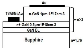
Optical wave-guiding in GaN, where the refractive index is 2.3 at wavelength of 1.5 µm, requires cladding layers of lower refractive index to confine light through the GaN core layer. In case of Si photonics, this confining of light wave is fulfilled by the utilization of Si thin films on top of low refractive index SiO2 buffer layer, which is thermally grown on bare Si substrate.
Fig. 3.1: GaN photonic circuits are built on ‘GaN on SiO2 on Si’ (GaNOI) substrates. Reproduced with
per-mission from Ref. [47].
Fig. 3.2: (a) Scanning Electron Micrograph of a cross section of a GaNOI waveguide (b) Optical trans-mission of a GaN microresonator. Reproduced with pertrans-mission from Ref. [48].
per the Fig. 3.1(a). Here, GaN photonic circuits are built on ‘GaN on SiO2 on Si’ substrate
(GaNOI). This GaNOI process works as: PECVD oxide is initially deposited on commercially available GaN on Si (111) wafers to assist the bonding process. Later on, the Si (111) layer is removed after bonding and new GaN surface undergoes a chemical-mechanical polishing (CMP) step reducing the GaN layer thickness.
A GaN microring resonator with 40 µm radii coupled with an input waveguide of width 860 nm was fabricated as mentioned in the paper. These two elements were separated by a 150 nm gap. These kinds of microrings are coupled critically at the telecommunication band of 1550 nm having extinction ratio of approximately 20 dB. By launching light from a tuneable infrared laser source and amplified with EDFA and by output light measurement using InGaAs photodetector, the optical response of this kind of photonic circuit can be estimated. It was also possible to get the phase matching between the fundamental light and the second harmonic light by waveguide width tuning. The technique used was 'multi-mode matching technique' [47].
3.2 Fabrication of GaN Waveguides on Silicon
Si substrates are low cost, extensively available in large diameter and have very good thermal and electrical properties. But still Si is not popular as substrate for the GaN photonics mainly due to cracking of GaN film for stress generation. This kind of stress is not so prominent for the SiC and sapphire substrates. The lattice mismatch between GaN and Si is about 16% which causes the dislocation density in the GaN layers but the important problem is high thermal mismatch which is about 54%. Again, Si has resistivity up to 104 ohm-cm which is very less than the
resistivity values of SiC or sapphire and that is why there is a possibility of parasitic capacitance effects at high frequency [49]. To make GaN based waveguides, membranes with high refractive index contrast is essential in between GaN and cladding layer mainly due to its low refractive index (it is 2.3 at 1.5 µm). However, for SOI based waveguides, the lower refractive index of SiO2 compared to Si provides sufficient refractive index contrast to confine the light within the
waveguide. Although the common substrates used in GaN waveguides are SiC, Si and sapphire but considering the under-etching technique, Si and SiC are better. SiC shows lower lattice mismatch (3.5%) compared to Si (17%) as substrate. But, the cost of SiC is comparatively higher. The use of Si is important for the goal of making integration of photonics and electronics in the same chips for their advantages of well-established technology, low cost and special optoelectronic properties of GaN. In case of GaN on Si technology, the refractive index of the underlying layer (nsi = 3.47) is higher than the GaN core (ngan= 2.3) layer at near-IR region. This
will stop the guiding of light through the waveguide unless there is some mechanism of suspended wire waveguide where the Si layer under the GaN wire is removed by dry etching. These wire waveguides are mechanically supported by the use of well-designed tethers.
Fig. 3.3: Fabrication process of a GaN based photonic crystal waveguide. Reproduced with permission from Ref. [50].
deposited on top of the structure by the process of PECVD. This SiO2 layer acts as a hard mask
for the entire fabrication process thereby protecting the GaN surface and the degradation of the pattern is stopped. Then, to pattern the previously spun positive photo-resist ZEP-520, the E-beam lithography is carried out. After the development of the resist, first the pattern is transferred to SiO2 by the process of fluorine-based Reactive Ion Etching (RIE). Then the pattern
is formed into AlN/GaN stacked layers by the process of chlorine based ICP (inductively coupled plasma) etching. By the dry process of fluorine based RIE, the membrane is released of the Si (111) substrate. Air gap in the order of 3 µm is achieved in this process which is sufficient to avoid the light loss through the substrate in the 1.5 µm band. At the final stage, the SiO2 layer
is released using the solution of hydrofluoric acid. This is the most critical stage for the fragility of the structure and very careful manipulation is required to avoid collapsing of the waveguide.
3.3 Optical Properties of GaN Waveguides
4 GaN Passive Waveguide Devices for Broadband Communication
In optical communication systems the ability of data manipulation / switching is important. There is a strong requirement to improve the speed of switching. There is a growing need for chip level optical systems where the data can be generated, modulated, and manipulated all-optically in the ultrafast fashion. The electro-absorption characteristics of GaN photonics have properties which can support very fast relaxation times suitable for ultrafast switching and properties to support lasing in the communication band. Moreover, as discussed in chapter 3, the GaN photonics is also CMOS compatible and the existing setups at factories might be used for mass production of devices.
4.1 Waveguide Basics
An optical waveguide is formed of a non-absorbing dielectric layer whose thickness is comparable to the wavelength of passing light and is deposited on a planar substrate. The thin film of the dielectric layer has the refractive index higher than the refractive index of the substrate. A variety of techniques are used for the growth of thin films such as metal organic chemical vapour deposition (MOCVD), molecular beam epitaxy (MBE), pulsed laser deposition, sputtering etc. These kinds of dielectric waveguides are used in various optical devices such as modulators, lasers, couplers, splitters etc. Typically, a GaN based novel dielectric waveguide is made of GaN semiconductor materials grown on sapphire. Waveguide structures can be constructed with GaN as the core with higher refractive index and AlxGa1-xN as the cladding
layer with lower refractive index. Here AlxGa1-xN is made by engineering the band-gap energy of
GaN and AlN alloys with different Al concentrations. Through this process, direct band-gap GaN semiconductor material and its alloys are used for the development of LEDs, lasers, photodetectors using the waveguides which are transparent for the spectrum of communication wavelength (1.5 µm). Importantly, the refractive indices of GaN materials and their alloys are important parameters for the design, fabrication and modelling of the above mentioned devices. There are different structures like buried rectangular, ridge and slab optical waveguides. These are shown in Fig. 4.1 [53].
Fig. 4.1: Examples of waveguides.
Fig. 4.2: A 2×2 directional coupler.
Y-branch beam splitters, tuneable TE/TM polarization splitters, power splitters and 1× N integrated splitters. All of these have versatile applications. For example, a single mode 3 dB Y-junction splitter which is symmetric has an important role in the development of integrated optics. This can be utilized in the splitting regions of the input and output ends as Mach-Zehnder interferometer. Waveguide couplers can be thought of connecting two Y-junction splitters connected oppositely.
A directional coupler is used to split or combine optical signals in a network. Figure 4.2 shows a 2×2 directional coupler. It has two input ports and two output ports. The figure shows that the power from one input port P0 or P3 can be split into two output ports P1 and P2.
4.2 Exploitation of Material Refractive Index in GaN Waveguides
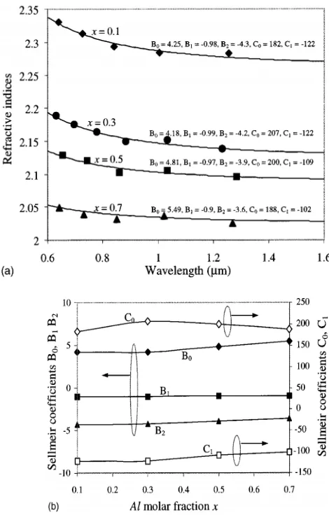
Knowledge of the material refractive index in the operating wavelength is important for designing an optically guided waveguide device. R. Hui et al. [54] followed a measurement technique in the design, fabrication and characterization of a single mode ridge optical waveguide device based on GaN/AlGaN hetero-structure. In his design initiative, a number of
film thickness ranges were from 1.1 to 1.5 µm and Al molar fraction ranges were from x = 0.1 to x = 0.7. The optical transmission spectra were then measured to evaluate the refractive index on each film. The optical transmission efficiency was wavelength dependent due to Fabry-Perot (FP) interference caused by two facets of the film (one is between AlxGa1-xN and the air and the
other is between AlxGa1-xN and sapphire). The film refractive index can be obtained from the
knowledge of the film thickness, by best fitting the measured optical transmission spectrum to a well-known FP transmission equation. For several different Al molar fractions, the measured refractive indices of AlxGa1-xN are shown in Fig. 4.3(a). In the figure, the continuous curves are
the numerical fittings using the first order Sellmeier dispersion formula as:
n(λ) = 1+ (!! ! !!! !!! !!)!!
!!!(!! ! !! !)! . (4.1)
The coefficients for best fit are shown in Fig. 4.3(a) and their variations versus Al molar fraction (x) are shown in Fig. 4.3(b).
For calculation of the refractive indices in 1550 nm wavelength, the information can be taken from Fig. 4.3. The following polynomial expression can be obtained for Al molar fraction (x) which has a dependence on the refractive index at 1550 nm:
n (1550 nm) = 0.431x2 – 0.735x + 2.335.
(4.2)
Here, the monotonic decrease of refractive index of AlxGa1-xN with the increase of Al molar
fraction helps for the design of the single mode waveguide devices.
A schematic diagram of a single mode waveguide cross-section based on GaN core and AlxGa1-xN cladding is shown in Fig. 4.4. A 4µm thick epitaxial film of AlxGa1-xN is grown on a
sapphire surface and a 3µm thick GaN is deposited on top of AlxGa1-xN layer. The optical
waveguide structures are formed by the process of lithographic pattern and inductively coupled plasma dry etching.
Fig. 4.3: (a) Refractive indices of AlGaN vs wavelengths for different Al molar fractions. (b) Sellmeir expression coefficient vs Al molar fractions. Reproduced with permission from Ref. [54].
[image:25.595.178.413.157.525.2]Fig. 4.4: Optical waveguide design using GaN/AlxGa1-xN hetero-structure grown on sapphire substrates: (a)
Waveguide Cross-section, (b) Single mode simulation, (c) Radiation pattern vs exit angle. Reproduced with permission from Ref. [54].
Fig. 4.5: Optical microscope image of GaN/AlxGa1-xN hetero-structure optical waveguide. Coupler: (a) Top
View (b) Cross-section at the output. Reproduced with permission from Ref. [54].
4.2.1 Birefringence of GaN Waveguide
In planar light wave circuits, it is important to have knowledge about refractive index changes, but at the same time the knowledge about birefringence of material is also important in the design and performance of waveguides. The birefringence of GaN film on sapphire was reported when a 4% refractive index change was observed due to changes of polarization of incident signal from perpendicular direction to the parallel direction to the c-axis crystal in the long wavelength (800nm) [55]. Again for the wurtzite crystalline structure, GaN possesses hexagonal configuration on c-axis. Due to variation of optical propagation direction on c-plane, the efficiency of optical propagation emission changes periodically. Hui, R. et al. investigated the birefringence on single mode GaN-AlGaN waveguides operating in 1550 nm telecommunication band [56]. They found that, the refractive index depends on the state of signal polarization and also on the direction of optical propagation in the c-plane. However, to avoid the need for polarization controller, birefringence in the waveguides needs to be minimised. Different ways to eliminate the effect of birefringence are: polarization compensation, introduction of tensile and compressive built-in stress during the process of growth and special waveguide cross-sectional design as mentioned in ref [56]. Stress engineering is the best option as it does not depend on device functionalities and configurations. This kind of stress may be caused by lattice mismatch, dislocation and impurity doping in the film. In the report, it is also mentioned that, with the variation of Al content, the light polarization in AlGaN film varies and the polarization property of AlN is different from that of GaN. This indicates another option of polarization control by the process of bandgap engineering [56].
4.2.2 Carrier-induced Index Change in GaN Waveguide
The carrier-induced refractive index change is the basic tuning process of PHASER based optical switching devices and it is faster than thermal tuning based devices [56]. To understand the efficiency in carrier based index changes in GaN semiconductors, three main carrier effects such as bandfilling, bandgap shrinkage and free carrier absorption will be discussed. By the term bandfilling, we understand the optical absorption decrease at energies slightly above the bandgap by the process of free carrier injection and impurity doping [56]. Optical absorption is a function of carrier concentration due to bandfilling. The carrier induced change in absorption coefficient can be expressed as [56]:
∆α (N, P, E) = α (N, P, E) – α0 (E). (4.3)
Here, ∆α (N, P, E) denotes the absorption coefficients at doped semiconductor with carrier injection and α0 is the intrinsic material absorption without injection. N and P denote the
∆n (N, P, E) = !!ħ !! 𝕽
∆!(!,!,É)
É!! !! !
! dÉ . (4.4)
Here, c, e and 𝕽 are the speed of light, electron charge and principal value of integral respectively. Because bandfilling decreases the absorption coefficient at a particular energy for all the cases, the material refractive index decreases due to bandfilling as well.
Bandgap shrinkage is caused by free injected carrier solely and not by doped carriers. For the increases of free carrier concentration for current injection, the conduction band energy decreases and the valance band energy increases. This happens as a result of the overlapping of electron wave functions, where a lower energy level gas of interacting electrons is formed at the bottom of conduction band and at the same time, a higher energy level gas of interacting holes is formed at the top of valance band. As a result, shrinkage of bandgap takes place for which a red shift of the absorption curve is generated.
The third carrier effect is known as free carrier absorption or plasma effect. In such a situation, a free carrier can absorb a photon and within the conduction band can move to a higher energy level. The changes in refractive index can be expressed as follows [57]:
∆n = !!.! × !"!!!
!!!
!
!!+𝑃
!!!!/!! !!"!/!
!!!!/!! !!"!/! . (4.5)
Here, n is the material refractive index, 𝑚!, 𝑚!! and 𝑚!! are the respective effective masses of electrons, heavy holes and light holes.
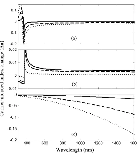
In Fig. 4.6, the curves show the refractive index changes vs wavelength due to bandfilling, band shrinking and carrier absorption effects. These calculations were carried out at three carrier injection levels of N = 7 × 1018 cm-3 as solid line, N = 3 × 1019 cm-3 as dashed line and 6 × 1019 cm-3 as dotted lines. For the cases of both bandfilling and bandgap shrinking, the curves are
Fig. 4.6: (a) Index change for bandfilling, (b) Band shrinking, (c) Free carrier absorption at N = 7 × 10¹⁸
cm-3 as solid line, N = 3 × 1019 cm-3 as dashed line and 6 × 1019 cm-3 as dotted lines, Reproduced with
permission from Ref. [56].
4.3 AWG for Multiplexing and De-multiplexing using GaN/AlGaN Hetero-structures
[image:29.595.199.429.152.410.2]
Fig. 4.7: (a) Overall index change vs wavelength at three carrier density levels (N = 7 × 1018 cm-3 as solid
line, N = 3 × 1019 cm-3 as dashed line and 6 × 1019 cm-3 as dotted lines). (b) Overall index change vs carrier
density at 1550 nm. Reproduced with permission from Ref. [56].
small in size which is difficult to materialize. Here, the interface between InP waveguide and optical fibre is difficult to achieve because of refractive index mismatch and mode spot size mismatch. The other disadvantage is the temperature sensitivity of refractive index which is about 10 times higher than that of silica. As such, the InP based AWGs are very sensitive to temperature changes and very meticulous temperature control is required for which these kinds of devices were not materialized commercially. GaN/AlGaN based AWGs are very advantageous compared to silica PLC and InP PLC for the application of wavelength tuning optical devices. In this case, the refractive index is less than 2.3 which is much close to that of silica and the intrinsic loss is less because of wide band gap in relation to the telecommunication band of 1.5 µm. In GaN/AlGaN materials, it is possible to make the hetero-junctions suitable for carrier injections. The application wavelength of 1.5 µm is far beyond the material band-gap and so; the optical loss at this wavelength will not be affected much by the carrier density change. However, the effective refractive index will be a function of carrier injection mainly due to free carrier absorption. That is the reason for materializing the fast tuneable GaN/AlGaN based AWG.
4.4 GaN Bragg Reflection Waveguides
Fig. 4.8: Schematic diagram of a Bragg Reflection Waveguide. Reproduced with permission from Ref. [62].
where the material dispersion is weaker especially at low frequency. Thereby, BRW features strong dispersive mode at low frequency in order to counter the strong dispersive mode at high frequency. This mechanism conserves the phase matching condition for Optical Parametric Amplification (OPA) over a broad range of wavelengths. Here, the χ(2) nonlinearity is used for
the generation of OPA with a goal of exploiting the entire available bandwidth (S, C, L) of communication band (1450-1600nm) [62].
A schematic diagram of Bragg Reflection Waveguide (BRW) geometry for non-degenerate OPA process having periodically poled GaN as core and periodic cladding layers of Al0.01Ga0.99N
(n1) and Al0.45Ga0.55N (n2) is shown in the Fig. 4.8. GaN is chosen here as a potential material
operating in a wide spectrum (365 nm – 13.6 µm), high nonlinear coefficient comparable to LiNbO3, high damage threshold and possibility of periodic poling to get Quadra Phase Matching
(QPM) conditions. Another advantage is that GaN does not exhibit photorefractive properties, which shows that these devices can be pumped with high-power visible radiation. In another example of a study on high index core symmetric Bragg reflection waveguide (BRW), efficient phase matched second-harmonic generation (SHG) was experimented [63].
4.5 GaN Photonic Crystal Waveguides
Fig. 4.9: Light propagation through a GaN photonic crystal waveguide. Reproduced with permission from
Ref. [67].
named as photonic crystal fibres (PCF) [68]. In a perfectly periodic lattice, the effect of impurity states also showed interesting properties in the band-gap which leads to the possibility of optical cavities for confining light in the photonic crystals [69]. In course of time, the idea of planar 2D photonic crystals was there [70, 71]. The photonic crystal effects act in two dimensions and that is why these are called 2D photonic crystal devices. The total internal reflection acts in the vertical dimension. To create a waveguide mode in a photonic crystal, it is possible to create a line defect by removing a row of holes from it. As a result, a mode of guidance through the spatial region is created from one end to the other end of the crystal within the waveguide but confined by the crystal lattice [72, 73]. This guided band which is discrete in nature falls inside the band gap. This is labelled as W1, W2 or Wn photonic crystal waveguides depending on the number of rows removed.
This photonic crystal W1 waveguide is important in the family of photonic crystal devices and shows a property of slow light near the band edge. It is also used effectively to couple the light in between the cavities embedded in the crystal lattices. A W1 photonic crystal waveguide based on GaN was designed and fabricated as shown in Fig. 4.9 [67].
4.6 GaN Nanowires as Waveguides
Fig. 4.10: Different structures of nanowires. Reproduced with permission from Ref. [75].
terials but only one dimensional characteristic. Their diameters are large enough that the quantum size effect is ignored and are not quantum wires. They can be found in the cross section of triangular, rectangular, hexagonal or cylindrical shapes as shown in Fig. 4.10 [75].
In a way, nanowires are very high quality unidirectional waveguides with high refractive index contrast from 2.5 to 3.5 between the wire and the surrounding layer, typically air [76]. Due to this high contrast, nanowires are very good waveguides with very small in diameter and length. It is possible to grow nanowires with or without epitaxial connection with a substrate [77]. In case of nanowires grown epitaxialy on a substrate, the crystal orientation of the substrate is automatically transferred to the nanowires that determine the direction and orientation of the nanowire growth. For this attribute, the lattice matching condition is greatly relaxed compared to the thin film growth. As such a higher strain can be tolerated. On the other hand, for the nanowire synthesis without epitaxial connection to substrates, the lattice matching condition is reduced further as any kind of substrate can be used for nanowire growth. For this reason of substrate insensitivity, nanowires open up new uses which are not common in planar systems. This strain relaxation of nanowire growth improves the design flexibility for the development of hetero-structure devices. This can be understood with the example of nanowire growth on Si as it will remain as preferred platform for different kinds of applications [46]. Si is available with large wafer area with very high crystal quality and purity. It is also mechanically stable and its material characterization is well known because of extensive investment made on Si technology. So, it is important to have a union between GaN material and Si which could render CMOS compatible devices with diversified functionalities. However, it is not easy to get the high quality growth of GaN thin films on Si. But, the mismatch problem has less consequence in crystal quality nanostructures because a very small diameter allows the strain to be relaxed laterally in contrast to the planar growth where the strain can only be relaxed along the one dimension [46].
these elements of different functionality and provide flexibility for the development of complex logic operations. Using the commercial micro-manipulators, the nanowires with sufficient lengths and strengths can be bent, pushed and shaped under optical microscope. Wires are flexible and can be reshaped to a coil of radii close to 5 µm which is not possible in case of bulk forms. Moreover, the nanowires can be easily shaped on the chosen surfaces with the support of wired substrates to avoid elastic recoil. These kinds of chemically synthesized nanowires are the building blocks for the making of nano-scale optoelectronic devices. In this way, the flexible nanostructures with precision positioning, optical waveguide linking and manipulation on surfaces with other nanowire elements are utilized to form optical networks and component devices.
To have an in-depth understanding of GaN nanowire growth, it is important to understand the crystal structure of GaN. GaN has the wurtzite structure as bulk under the ambient condition which is also thermodynamically stable. Wurtzite structure is hexagonal unit cell with two lattice constants c and a [79]. The stacking order or the order of GaN and N atom layers on top of another layer in c direction can be represented by GaANAGaBNBGaANAGaBNB... .
Various growth processes, such as Laser assisted growth, Chemical Vapour Deposition (CVD), Anodic alumina template synthesis and Molecular Beam Epitaxy (MBE) are there for GaN nanowires [79]. These can be performed with the help of metal catalysts or without of them. For Chemical vapour deposition method, nanowires grow along the a-axis of wurtzite phase, whereas, in MBE method, nanowires grow along the c-axis. More often than not, small particles of a foreign material are used to help the nanowire growth in these methods. This growth mechanism is also named as catalytic growth and it has two techniques namely, vapour-liquid-solid (VLS) or vapour-solid-solid mainly depending on the particle (liquid or solid) phases. As for example, in case of VLS, the growth starts from liquid metal catalyst [79, 80]. Here, the metal catalyst of nanometre size is deposited on a substrate utilizing the techniques like laser ablation, thermal annealing, electrochemical deposition, colloidal dispersion etc.
5 GaN Active Waveguide Devices for Broadband Communication
Quantum wells are the structures consisting of thin well materials sand-witched by two layers of barrier materials. Optical properties of quantum well depend on the photon energy of two materials (well and barrier materials) and their thickness. In the materials, lattice mismatch produces the straining effect. Due to excess strain, the material quality is degraded as it develops cracks. This critical value of strain depends on the thickness of the layer and also on the magnitude of the lattice mismatch. It seems that the thick layer needs to be accurately lattice-matched but the thin layer as seen in the quantum wells can be severely strained without significant degradation of the material quality (Page: 2-3, The Handbook of Photonics, 2nd Ed, Mool C. Gupta, John Balloto) [81]. In GaN/AlN quantum wells, GaN is the ‘well’ and it is sandwiched by AlN ‘barriers’. In the wells, both electrons and holes see lower energy. This layer is very thin and electrons and holes may be considered as waves. The allowed states in the structure correspond to the standing waves working in perpendicular direction of the layers. Using the Multiple Quantum wells (MQW) of such materials, two types of all-optical switching can be performed - one being ‘Inter-band transition by inter sub-band transition’ and the other is ‘Inter sub-band transition by inter sub-band transition’ [82].
5.1 GaN Waveguides with Quantum Wells and Characteristics
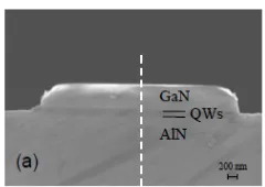
Fig. 5.1: A SEM image of the facet of a GaN/AlN QW waveguide. Reproduced with permission from Ref. [84].
Fig. 5.2: (a) Signal transmittance through a GaN QW waveguide versus signal-control delay time for different.
type of waveguide are discussed. The inter sub-band (ISB) transition of this type of QW in the near-infrared band shows: (i) ultrafast relaxation lifetime, (ii) very large conduction-band offset, (iii) large optical nonlinearity and (iv) promises of monolithic integrated platforms [83]. High power control pulses were used to modulate the ISB absorption losses of a weaker input optical signal. Both the signal and control pulses are generated by the same mode-locked fibre laser having 160 fs pulse width and TM polarization mode. The plot for signal transmittance versus signal control delay time through the waveguide (1 mm long and 3 µm wide) is shown in Fig. 5.2(a) [83]. This plot was traced for different energies of control pulses. The signal modulation depth versus control pulse energies is also plotted as shown in Fig. 5.2(b). From the plot, it is seen that the switching requirement to obtain 10-db modulation depth is about 38 pJ.
[image:36.595.237.357.155.240.2]Fig. 5.3: Signal Transmittance versus signal-control delay time for different control pulse energies. Reproduced with permission from Ref. [83].
timing jitter seen in the measurement mainly due to the laser source. With better laser source, faster ISB relaxation time is expected in the QW of the waveguides. The absorption saturation in these types of quantum well waveguides is generally accompanied by ultrafast refractive index modulation which is related to same inter-subband carrier dynamics. A plot of self-phase modulation is shown in the Fig. 5.3 [83]. Here the optical spectra of transmitted ultra-fast pulses through the waveguide for different energies of input pulses are shown. However the shapes are governed by the interaction of the dispersion and nonlinear refraction. Spectral broadening with the increases of input pulse energy occurs if the pulses are TM polarized and coupled to ISB transition. Here the inter sub-band refractive index modulation or phase modulation induced by the pulses takes place. On the other hand, there is no change in the spectral shape if the pulses are TE polarized which also confirms the ISB nonlinear process in the QW waveguides. This refractive index nonlinearity can be further used for optical switching platform by utilizing an interferometric configuration to convert phase to amplitude modulation [83].
5.2 Optical Nonlinearity in GaN/AlGaN Quantum Wells


![Fig. 4.10: Different structures of nanowires. Reproduced with permission from Ref. [75]](https://thumb-us.123doks.com/thumbv2/123dok_us/1574214.110018/33.595.219.378.158.269/fig-different-structures-nanowires-reproduced-permission-ref.webp)