A Comprehensive Analysis on Data Hazard for RISC32 5-Stage Pipeline Processor
Wei Pau Kiat, Kai Ming Mok, Wai Kong Lee, Hock Guan Goh & Ivan Andonovicy*
Faculty of Information and Communication Technology Universiti Tunku Abdul RahmanKampar, Malaysia *Department of Electronic and Electrical Engineering University of Strathclyde, Glasgow, G1 1XW, UK
Email: [email protected], [email protected], [email protected], [email protected], *[email protected]
Abstract—This paper describes the verification plan on data hazard detection and handling for a 32-bit MIPS ISA (Microprocessor without Interlocked Pipeline Stages Instruction Set Architecture) compatible 5-stage pipeline processor, RISC32. Our work can be used as a reference for RISC32 processor developers to identify and resolve every possible data hazard that might arise during execution phase within the range of the basic MIPS core instruction set. All the respective data hazard has been tested and verified. The techniques used to resolve data hazard in this paper are data forwarding and pipeline stages stalling. When data hazard arises, it is first resolve by using data forwarding. If the problem persists, we use pipeline stages stalling then only follow by another data forwarding to resolve the data hazard. This combination will reduce the impact of data hazard on the processor throughput, instead of only using the pipeline stages stalling. This paper delivers a comprehensive analysis and the development of the data hazard resolving blocks that are able to resolve data hazard arises from basic MIPS core instruction set in RISC32 processor.
Keywords—Data Hazard, MIPS, Pipeline, Data Forwarding, Interlock Pipeline Stages
1. Overview
The pipeline hazards can be classified into 3 types, structural hazard, control hazard and data hazard [1], [3], [6]. Data hazards always exist in a processor designed based on pipeline approach. It can cause computational error when multiple instructions are overlapped during its execution which involve accessing the processor’s system registers, (e.g. Register File (RF), interrupt controller (CP0) registers and HILO register). In contrast, single-cycle and multi-cycle processor are immune to this situation since consecutive instruction only execute after the current instruction finished its whole execution. Although data hazard exists in pipeline processor and it require extra hardware to resolved, the high performance achieved by pipelined processor still outweighs its counter parts and remains a popular choice in processor design.
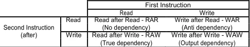
[image:1.612.320.563.240.286.2]Data hazard occurs due to data dependency, whereby an instruction attempts to read or write system register before the valid data are available for reading. The data dependency relationship is shown in the Table 1.
TABLE 1. DATA DEPENDENCY RELATIONSHIP
First Instruction
Read Write
Read Read after Read - RAR Write after Read - WAR
Second Instruction (No dependency) (Anti dependency)
(after) Write Read after Write - RAW Write after Write - WAW
(True dependency) (Output dependency)
From Table 1, there are 3 types of data dependency that leads to data hazard. Both Write-after-Read (WAR) and Write-after-Write (WAW) dependencies will never occur when the pipeline processor only allows system registers to be updated at a specific stage.
We observed that Read-after-Write (RAW) dependency causes majority of the data hazards. In RISC32 convention, Register File (RF) will only be updated at the fifth (Write-Back (WB)) stage. Since read (ID stage) and write (WB stage) to RF is occurred in two different stages, an instruction may attempt to read RF before it is updated with the latest data. This condition can be resolved in several ways, generally classified into software and hardware approach.
There is no existing works that populate all the combinations of instructions that might cause data hazard. Hence, we are motivated to perform thorough analysis on data hazard detection and handling scheme for RISC32 processor which we strongly believe will benefit others with similar interest in processor development.
This paper is organized as follows: Section 2 describes the background of our work. Section 3 describes the processor micro-architecture requirements prior to resolve data hazards. Section 4 and 5 describe the process of resolving data hazard using forwarding and interlock scheme respectively. Lastly, Section 6 concludes the finding of our paper.
2. Background
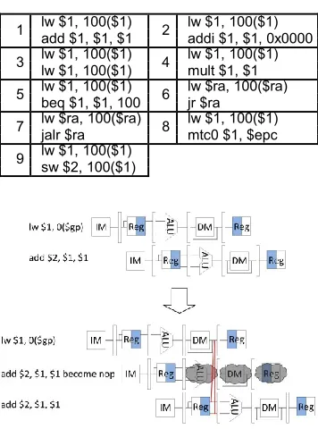
The pipeline processor, RISC32, which we have developed, is based on 5-cycle instruction execution, which corresponds to 5 hardware stages: Instruction Fetch (IF), Instruction Decode and Register File Read (ID), Execution or address calculation (EX), Data Memory Access (MEM) and Write Back (WB). Figure 1 illustrates the situation where data hazard occurs in a RISC32 processor.
to forward the data to the consecutive instructions. Both last (sw) and second last (add) instructions do not cause any data hazard since the data is written into the RF at the first half of the clock cycles and it is ready for reading in the second half of the clock cycles.
[image:2.612.341.525.269.360.2]There are also some data hazard conditions that cannot be resolved by only using data forwarding technique [1], [4], [5]. Consider the load-use data hazard illustrated in Figure 3. The first instruction (lw) accesses the data memory at the fourth (MEM) stage and the data is only ready at the end of the fourth stage. At the same time, the consecutive instruction (and) already reaches third (EX) stage with the operand values that have not been updated yet by the lw instruction. As a result, the processor needs to stall for 1 clock cycle before data forwarding can correctly take place. Figure 4 illustrates the load-use data hazard resolved by pipeline stages stalling followed by data forwarding.
Figure 1. MIPS Pipelined Data Hazard (Taken from [1])
[image:2.612.67.276.321.435.2]Referring to Figure 1, the first instruction (sub) is supposed to update the register $2 with the latest result at the WB stage, but the second (and), third (or) and fourth (add) instructions attempt to read the register $2 before it is updated. This implies that all the subsequent computations will be based on the wrong result.
Figure 2. Illustration of Data Forwarding (Taken from [1])
Figure 2 illustrates the use of data forwarding [1], [2], [3], [4] to resolve the data hazards. The result of the first instruction (sub) is generated at the end of the EX stage and will be registered into the EX/MEM pipeline, so it is possible
[image:2.612.345.526.395.487.2]Figure 3. Illustration of Load-use Data Hazard (Taken from [1])
Figure 4. Pipeline Stages Stalling and Data Forwarding to Resolve Load-use Data Hazard (Taken from [1])
The work presented by Patterson et al. [1], Mohit et al. [3], Gautham et al [4] and Zulkifli et al. [5] generalized the concept of data hazard based on the RF which we have further extended it into interrupt controller unit (CP0) registers and multiplier HILO register. The extended version provides comprehensive verification coverage for the data hazard based on the RISC32 processor and is useful for the micro-architecture development. Our work also includes miscellaneous scenario: the data hazard related to the unconditional branch (jal and jalr) with $ra register (return address register).
[image:2.612.70.275.536.646.2]and J-type instructions were not included in their resolving and benchmarking scheme.
In this paper, we will provide comprehensive verification coverage on data hazard for RISC32 processor and the resolving scheme using data forwarding and pipeline stages stalling techniques.
3. Processor
3.1. Micro-architecture
The scope of our work in data hazard analysis includes not only the Register File, but also extended with the multiplier and interrupt controller, (CP0) registers. This requires new instructions and with their corresponding system registers, to hold the new type of data which unavoidably introduce new data hazard. The processor micro-architecture is shown in the Figure 5.
The multiplier unit, based on Booth algorithm requires 2 cycles (EX and MEM stages) to compute a result which will be available at the end of the MEM stage and will be written to the HILO register at the first half cycle of the WB stage.
For the CP0, data will be read from CP0 register at ID stage and write to CP0 register at the EX stage. Writing to CP0 register occurs in EX stage, which does not follow the convention used for RF (write at WB stage). The purpose to write to CP0 register in an earlier stage is to avoid additional data hazard cause by the mtc0 instruction immediately followed by mfc0 instruction accessing the same CP0 register. Hence, data forwarding circuitry can be reduced. Figure 6 illustrates our approach to resolve the data hazard discussed. Note that the CP0 register is updated at the first half of the cycle and ready to be access at the second half of the cycle of EX stage.
[image:3.612.66.288.510.568.2]The forwarding and interlock blocks were developed to handle data hazard as shown in Figure 5. The forwarding block is responsible to forward data among stages while interlock block is responsible to stall the IF and ID stages and flush the EX stage for one clock cycle when a load-use hazard is detected.
Figure 6. Interrupt controller register related Data Hazards Abstract view
3.2. Control Unit Signals Related to Data Hazard
Before handling data hazard, the processor will need to identify what instructions have entered into the execution state. Table 2 describes function of the control unit signal and Table 3 presents the signal representation for the respective instructions. All the control unit signals are
TABLE 2. CONTROL UNIT SIGNAL FUNCTIONAL DESCRIPTION
Control Unit Signal Function
ID.mfc0 mfc0 instruction issued
ID.jal jal instruction issued
ID.jalr jalr instruction issued
ID.mult mult instruction issued
ID.hilo Either mflo or mfhi instruction issued
ID.hi2rf mfhi instruction issued
ID.rf wr Set when requires write-back to Register File
ID.load Load memory’s data instruction issued ID.store Store memory’s data instruction issued
generated at the ID stage and transfer along stages for data hazard detection.
4. Forwarding Scheme
Data forwarding technique is divided into two stages: detection and resolve. In the following subsection, we present the analysis and verification of all the combination of instructions that causes data hazards.
4.1. Data Hazard Detection Conditions
We have divided the data hazard detection into 5 groups in relation to the system registers: General Condition of Register File, $ra register, Load-store, HILO Register and CP0 Registers Related Data Hazards.
4.1.1. General Condition of Register File Related Data Hazards.
The work presented by [1], [2], [3], [4] suggested that the data is forwarded from MEM or WB stages to EX stage. However, in our design, the data forwarding is performed one stage earlier, that is from EX or MEM stages to ID stage. This can reduce the power consumption and pipeline size due to lesser control unit signals passing through the pipeline structure. Another small advantage is to balance the stage propagation delay of ID and EX stage: the propagation delay of ALU in EX stage is longer than RF in ID stage [8]. The Figure 7 shows the abstract view of the data forwarding for the condition discussed.
Figure 7. General Condition of Register File Related Data Hazards Abstract view
[image:3.612.347.532.523.590.2]Figure 5. RISC32 Pipelined Processor Micro-Architecture
TABLE 3. PROCESSOR CONTROL SIGNAL
Addressing
Format Instruction(s) ID.mfc0 ID.jal ID.jalr ID.mult ID.hilo ID.hi2rf ID.rf wr ID.load ID.store
Register add, and, or 0 0 0 0 0 0 1 0 0
Register mult 0 0 0 1 0 0 0 0 0
Register mflo 0 0 0 0 1 0 1 0 0
Register mfhi 0 0 0 0 1 1 1 0 0
Register jalr 0 0 1 0 0 0 1 0 0
Register mfc0 1 0 0 0 0 0 1 0 0
Immediate addi, andi, ori 0 0 0 0 0 0 1 0 0
Base lw, lhu, lh, lb 0 0 0 0 0 0 1 1 0
Base sw, sh, sb 0 0 0 0 0 0 0 0 1
Pseudodirect jal 0 1 0 0 0 0 1 0 0
4.1.2. Register File related Data Hazards - $raregister.
This condition arises when the processor issued an unconditional branch instruction such as jump and link, (jal) and jump and link register, (jalr) which updates the $ra register with the address of the next instruction (PC+4). However, the consecutive instruction right after jal or jalr will read the old value of $ra register at ID stage. This situation is shown in Figure 8.
Figure 8. $ra register related Data Hazards Abstract view
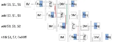
TABLE 4. General Condition of Register File Related Data Hazards
1 add $1, $1, $1 2 addi $1, $1, 0x0000
add $1, $1, $1 add $1, $1, $1 add $1, $1, $1 addi $1, $1, 0x0000
3 nop 4 nop
add $1, $1, $1 add $1, $1, $1 5 add $1, $1, $1addi $1, $1, 0x0000 6 addi $1, $1, 0x0000addi $1, $1, 0x0000
add $1, $1, $1 addi $1, $1, 0x0000
7 nop 8 nop
addi $1, $1, 0x0000 addi $1, $1, 0x0000 9 add $1, $1, $1lw $1, 100($1) 10 addi $1, $1, 0x0000lw $1, 100($1) add $1, $1, $1 addi $1, $1, 0x0000
11 nop 12 nop
lw $1, 100($1) lw $1, 100($1) 13 add $1, $1, $1 14 addi $1, $1, 0x0000
sw $1, 100($1) sw $1, 100($1) add $1, $1, $1 addi $1, $1, 0x0000
15 nop 16 nop
sw $1, 100($1) sw $1, 100($1) 17 add $1, $1, $1beq $1, $1, 100 18 addi $1, $1, 0x0000beq $1, $1, 100
add $1, $1, $1 addi $1, $1, 0x0000
19 nop 20 nop
beq $1, $1, 100 beq $1, $1, 100 21 add $ra, $ra, $rajr $ra 22 addi $ra, $ra, 0x0000jr $ra
add $ra, $ra, $ra addi $ra, $ra, 0x0000
23 nop 24 nop
jr $ra jr $ra
25 add $1, $1, $1mult $1, $1 26 addi $1, $1, 0x0000mult $1, $1 add $1, $1, $1 addi $1, $1, 0x0000
27 nop 28 nop
mult $1, $1 mult $1, $1 29 add $1, $1, $1mtc0 $1, $epc 30 addi $1, $1, 0x0000mtc0 $1, $epc
add $1, $1, $1 addi $1, $1, 0x0000
31 nop 32 nop
mtc0 $1, $epc mtc0 $1, $epc 33 add $ra, $ra, $rajalr $ra 34 addi $ra, $ra, 0x0000jalr $ra
add $ra, $ra, $ra addi $ra, $ra, 0x0000
35 nop 36 nop
jalr $ra jalr $ra lw $1, 100($1) lw $1, 100($1)
37 nop 38 nop
lw $1, 100($1) sw $1, 100($1) lw $1, 100($1) lw $1, 100($1)
39 nop 40 nop
mult $1, $1 mult $1, $1 lw $1, 100($1) lw $1, 100($1)
41 nop 42 nop
jr $ra jalr $ra
lw $1, 100($1) 43 nop
mtc0 $1, $epc
4.1.3. Register File related Data Hazards - Load-store.
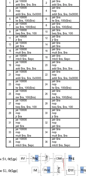
A store hazard has the similar characteristics as load-use hazard, which the RAW dependency exists between the combinations of instructions started with a load instruction. However it can be resolved by using data forwarding. By referring to the MIPS ISA convention, the registers used for load and store instruction can be classified into two usages, one for holding address ($rs) and another for holding data ($rt). Address calculation of the store instruction is performed at the EX stage: $rs should be ready before going into the ALU unit for address calculation. Since the data of the load instruction is only available at the MEM stage onwards, it requires pipeline stages stalling when the consecutive instruction relies on the respective data to perform calculation in the EX stage. In contrast, for the case where the store instruction not using the data of the load instruction in the EX stage but requires the data at MEM stage, it can be resolve using data forwarding and this is illustrated in Figure 9. The data can be forwarded from the MEM stage to EX stage of the consecutive instruction. The detection and handling of this hazard will be discussed in Section 4.2.
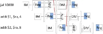
TABLE 5. $RA REGISTER RELATED DATA HAZARDs
1 jal 10000add $ra, $ra, $ra 2 jalr $raadd $ra, $ra, $ra jal 10000 jalr $ra
3 nop 4 nop
addi $ra, $ra, 0x0000 addi $ra, $ra, 0x0000 5 jal 10000lw $ra, 100($ra) 6 jalr $ralw $ra, 100($ra)
7 jal 10000sw $ra, 100($ra) 8 jalr $rasw $ra, 100($ra)
9 jal 10000beq $ra, $ra, 100 10 jalr $rabeq $ra, $ra, 100
11 jal 10000jr $ra 12 jalr $rajr $ra
13 jal 10000jalr $ra 14 jalr $rajalr $ra
15 jal 10000mult $ra, $ra 16 jalr $ramult $ra, $ra
17 jal 10000mtc0 $ra, $epc 18 jalr $ramtc0 $ra, $epc jal 10000 jalr $ra
19 nop 20 nop
add $ra, $ra, $ra add $ra, $ra, $ra jal 10000 jalr $ra
21 nop 22 nop
addi $ra, $ra, 0x0000 addi $ra, $ra, 0x0000 jal 10000 jalr $ra
23 nop 24 nop
lw $ra, 100($ra) lw $ra, 100($ra) jal 10000 jalr $ra
25 nop 26 nop
sw $ra, 100($ra) sw $ra, 100($ra) jal 10000 jalr $ra
27 nop 28 nop
beq $ra, $ra, 100 beq $ra, $ra, 100 jal 10000 jalr $ra
29 nop 30 nop
jr $ra jr $ra
jal 10000 jalr $ra
31 nop 32 nop
jalr $ra jalr $ra jal 10000 jalr $ra
33 nop 34 nop
mult $ra, $ra mult $ra, $ra jal 10000 jalr $ra
35 nop 36 nop
[image:5.612.104.248.96.460.2]mtc0 $ra, $epc mtc0 $ra, $epc
Figure 9. Load-store Data Hazards Abstract view
4.1.4. HILO Register Related Data Hazards.
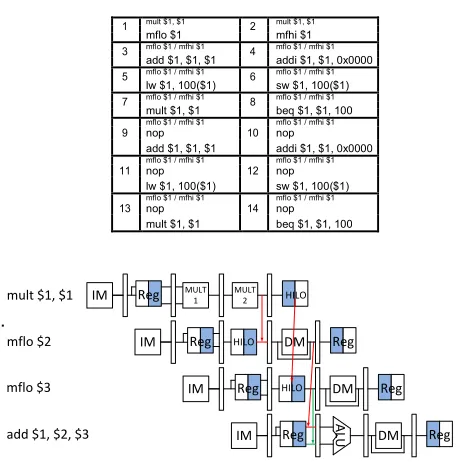
New instructions are needed to move the multiplication result (register HI and LO) to the RF before it can use by other instructions. The new instructions are: move from LO register (mflo) and move from HI register (mfhi). The multiplication related data hazard may arise in two scenarios.
Scenario 1: when after multiplication, the result is to be read by either mflo or mfhi, but it is not ready for reading until at the WB stage. For example, in Figure 10, data hazard occurs between the first (mult) and second (mflo) instructions and the multiplication result should be forwarded from MEM stage to EX stage.
Scenario 2: when the processor copies the HILO register’s data to the RF, reading the same register in the RF before it is updated. For example, in Figure 10, data hazards occurs between second (mflo) (or third (mflo)) and fourth (add) instructions, and the HILO register’s data should be forwarded from the EX or MEM stage to ID stage.
DM
IM Reg MULT1 MULT2 HILO
IM HILO Reg
mult $1, $1
mflo $2
mflo $3 IM HILO Reg
IM DM
A
LU
Reg Reg
add $1, $2, $3
Reg
[image:6.612.54.286.82.313.2]Reg DM
TABLE 6. HILO REGISTER RELATED DATA HAZARD TABLE 7. CP0 REGISTERS RELATED DATA HAZARD
1 mult $1, $1 2 mult $1, $1 1 mfc0 $1, $epc 2 mfc0 $1, $epc
mflo $1 mfhi $1 add $1, $1, $1 addi $1, $1, 0x0000
3 mflo $1 / mfhi $1 4 mflo $1 / mfhi $1 3 mfc0 $1, $epc 4 mfc0 $1, $epc
add $1, $1, $1 addi $1, $1, 0x0000 lw $1, 100($1) sw $1, 100($1)
5 mflo $1 / mfhi $1 6 mflo $1 / mfhi $1 5 mfc0 $1, $epc 6 mfc0 $1, $epc
lw $1, 100($1) sw $1, 100($1) beq $1, $1, 100 jr $ra
7 mflo $1 / mfhi $1 8 mflo $1 / mfhi $1 7 mfc0 $1, $epc 8 mfc0 $1, $epc
mult $1, $1 beq $1, $1, 100 mtc0 $1, $epc mult $1, $1
mflo $1 / mfhi $1 mflo $1 / mfhi $1 mfc0 $1, $epc mfc0 $1, $epc
9 nop 10 nop 9 jalr $ra 10 nop
add $1, $1, $1 addi $1, $1, 0x0000 jalr $ra
mflo $1 / mfhi $1 mflo $1 / mfhi $1 mfc0 $1, $epc mfc0 $1, $epc
11 nop 12 nop 11 nop 12 nop
lw $1, 100($1) sw $1, 100($1) add $1, $1, $1 addi $1, $1, 0x0000
mflo $1 / mfhi $1 mflo $1 / mfhi $1 mfc0 $1, $epc mfc0 $1, $epc
13 nop 14 nop 13 nop 14 nop
mult $1, $1 beq $1, $1, 100 lw $1, 100($1) sw $1, 100($1)
mfc0 $1, $epc mfc0 $1, $epc
15 nop 16 nop
beq $1, $1, 100 jr $ra mfc0 $1, $epc mfc0 $1, $epc
17 nop 18 nop
mtc0 $1, $epc mult $1, $1 .
Figure 10. HILO Register Related Data Hazards Abstract view
4.1.5. CP0 Registers Related Data Hazards.
Two instructions are added in order to access CP0 registers, which are move from CP0 register, (mfc0) and move to CP0 register, (mtc0). The data hazard of the CP0 register arises in the same pattern, which always start with mfc0 instruction. The first instruction in Figure 11 will get the CP0 register’s data at ID stage and write to RF at WB stage. The data hazard arises when CP0 register’s data is copied to RF’s register while at the same time, the respective register in the RF is occupied for further computation. Referring to Figure 10, the CP0 register’s data is available to be forwarded from EX or MEM stages to ID stage to avoid for data hazard. Table 7 cover the combinations of instructions grouped under CP0 registers related data hazard.
Figure 11. CP0 Register Data Forwarding Abstract view
4.2. Development of the Forwarding Block:
Detection and Handling
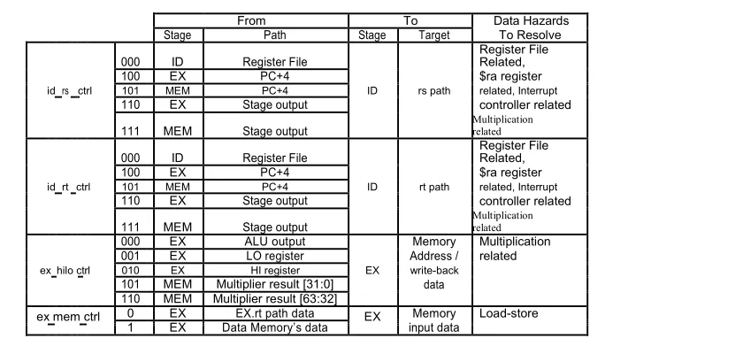
By observing all the data hazard detection conditions discussed, there are four data paths used as the target of data forwarding. The first two paths are the rs and rt path. which are used to pass ID, EX and MEM stage data to ID stage. These two paths are used to resolve the General Condition of Register File, $ra register, CP0 registers and HILO register related data hazards. 3-bit control signal is
used to select which source be forwarded. The Most Significant Bit (MSB) of the signal indicates the condition of the data, whereby 0 indicate normal flow without data forwarding and else otherwise. The third path is the hilo path, which is used to forward MEM stage data to EX stage. It is meant to resolve the first scenario of the HILO register related data hazards discussed. The same convention of rs and rt path applies to hilo path. The 3-bit control signal is used and the MSB indicates the condition of the data. 001 and 010 of the ex_hilo_ctrl in Table 8 is used to transfer the HI or LO register’s data when issue mfhi or mflo instruction respectively. On the other hand, 000 indicates that instructions other than mfhi and mflo were issued. It is to avoid duplicated logic and reduce the multiplexer used to transfer the data from stage to stage. The last path is used to resolve load-store data hazard. This path forwards the data from the MEM stage. 1-bit control signal is used to indicate the condition of the data, whereby 1 represent the data is forwarding from other stage and else otherwise. Table 8 shows the information of the data paths used for data forwarding.
[image:6.612.372.505.87.238.2] [image:6.612.56.267.522.589.2]TABLE 8. DATA FORWARDING HANDLING SCHEME
From To Data Hazards
Stage Path Stage Target To Resolve
000 ID Register File Register File Related,
100 EX PC+4 $ra register
id rs ctrl 101 MEM PC+4 ID rs path related, Interrupt
110 EX Stage output controller related
111 MEM Stage output Multiplication related
000 ID Register File Register File Related,
100 EX PC+4 $ra register
id rt ctrl 101 MEM PC+4 ID rt path related, Interrupt
110 EX Stage output controller related
111 MEM Stage output Multiplication related
000 EX ALU output Memory Multiplication
001 EX LO register Address / related
exhilo ctrl 010 EX HI register EX write-back
101 MEM Multiplier result [31:0] data
110 MEM Multiplier result [63:32]
ex mem ctrl 0 EX EX.rt path data EX Memory Load-store
1 EX Data Memory’s data input data
5. Interlock scheme
In this paper, the interlock scheme is further extended to avoid stalling the pipeline stages when resolving data hazard (with data forwarding scheme) for the load-store condition. Besides that, based on our finding, the interlock block might not work well after extended with CP0, which is a load instruction followed by mfc0 instruction. It may stall the pipeline even there is no data hazard arises. The following detection conditions highlight the problem discussed.
5.1. Data Hazard Detection Conditions
For some of the load-use conditions, it may not cause data hazard while the interlock block is still inserting a delay slot. It may unnecessarily reduce the processor throughput since it inserts an unnecessary load delay on the load-use combination of instructions that doesn’t cause any data hazard. To resolve this problem, special condition should be set case by case. Based on our finding, only the combination of load-use instructions shown in Table 8 will causes data hazard and require a delay slot to resolve. One cycle after the delay slot, the data in Data Memory should be available and ready to be forwarded to the next consecutive instructions. The forwarding scheme in the previous section should be able to handle the consecutive data hazard arises. Figure 12 illustrates the load-use data hazard solved by combination of pipeline stalling followed by data forwarding scheme.
5.2. Development of the Interlock Block:
Detection and Handling
[image:7.612.133.553.82.282.2] [image:7.612.57.300.151.637.2]TABLE 9. LOAD-USE DATA HAZARDs
1 lw $1, 100($1)add $1, $1, $1 2 lw $1, 100($1)addi $1, $1, 0x0000
3 lw $1, 100($1)lw $1, 100($1) 4 lw $1, 100($1)mult $1, $1
5 lw $1, 100($1)beq $1, $1, 100 6 lw $ra, 100($ra)jr $ra
7 lw $ra, 100($ra)jalr $ra 8 lw $1, 100($1)mtc0 $1, $epc
9 lw $1, 100($1)sw $2, 100($1)
Figure 12. Combination of Pipeline Stages Stalling and Data Forwarding for Resolving Load-use Hazards
6. Conclusion
In this paper, we presented a thorough analysis on data hazard of 32-bit MIPS ISA compatible 5-stage pipeline processor and the overall resolving scheme to handle basic MIPS core instruction set data hazards that might arise. The analysis shown here can serve as a reference for MIPS ISA compatible pipeline processor developers to eliminate all the data hazards. All the data hazards should be resolved prior to further development as the data correctness is extremely important. Furthermore, based on our experience, it is troublesome to capture a data hazard when the processor is integrated with I/O system and memory system, whereby data correctness is critical.
We intended to develop a pipeline processor for Internet-of-Things (IoT) in future, which is mostly going to handle largeamount of data, including data collection from sensors, data aggregation and data transmission to another device. Therefore, data correctness is critical to IoT and hence we provide this paper as the useful information to resolve basic MIPS core instruction set data hazard that might arises in processor level.
Acknowledgments
This research work is fully supported by UTAR Research Fund (UTARRF), Malaysia under grant IPSR/RMC/UTARRF/2015-C2/G01.
References
[1] Patterson, D. A., Hennessy, J. L., ”Computer Organization and De-sign: The Hardware/Software Interface”, 5th edition, ISBN: 978-0-12-407726-3, 2014
[2] S. P. Ritpurkar, M. N. Thakare and G. D. Korde, ”Design and sim-ulation of 32-Bit RISC architecture based on MIPS using VHDL,” Advanced Computing and Communication Systems, 2015 International Conference on, Coimbatore, 2015, pp. 1-6.
[3] M. N. Topiwala and N. Saraswathi, ”Implementation of a 32-bit MIPS based RISC processor using Cadence,” Advanced Communication Control and Computing Technologies (ICACCCT), 2014 International Conference on, Ramanathapuram, 2014, pp. 979-983.
[4] P. Gautham, R. Parthasarathy and K. Balasubramanian, ”Low-power pipelined MIPS processor design,” Proceedings of the 2009 12th International Symposium on Integrated Circuits, Singapore, 2009, pp. 462-465.
[5] M. Zulkifli, Y. P. Yudhanto, N. A. Soetharyo and T. Adiono, ”Reduced stall MIPS architecture using pre-fetching accelerator,” 2009 Interna-tional Conference on Electrical Engineering and Informatics, Selangor, 2009, pp. 611-616.
[6] P. V. S. R. Bharadwaja, K. R. Teja, M. N. Babu and K. Neelima, ”Advanced low power RISC processor design using MIPS instruction set,” Electronics and Communication Systems (ICECS), 2015 2nd International Conference on, Coimbatore, 2015, pp. 1252-1258.
[7] Meng-Chou Chang and Da-Sen Shiau, ”Comparison of two data hazard handling schemes for asynchronous pipelined processors,” Computer Science and Information Technology (ICCSIT), 2010 3rd IEEE Inter-national Conference on, Chengdu, 2010, pp. 36-40. [8] D. M. Harris and S. L. Harris, “Digital design and computer
![Figure 3. Illustration of Load-use Data Hazard (Taken from [1])](https://thumb-us.123doks.com/thumbv2/123dok_us/1464677.99117/2.612.341.525.269.360/figure-illustration-load-use-data-hazard-taken-from.webp)