High Extinction ratio TE/TM selective Bragg grating
filters on silicon-on-insulator
C
HARALAMBOSK
LITIS1,*, G
IUSEPPEC
ANTARELLA2, M
ICHAELJ. S
TRAIN2,
ANDM
ARCS
OREL11School of Engineering, University of Glasgow, Glasgo G12 8LT, UK 2Institute of Photonics, University of Strathclyde, Glasgow G1 1RD, UK *Corresponding author: [email protected]
Compiled July 5, 2017
We report on the design and fabrication of TE and TM polarisation selective Bragg gratings filters in the form of sinusoidal perturbations on the waveguide sidewall and etched holes on the top of the waveguide respec-tively. Combining the two geometries on a silicon-on-insulator waveguide resulted in Bragg grating filters with high extinction ratios of approximately 60 dB. © 2017 Optical Society of America
OCIS codes: (130.0130)Integrated optics; (130.5440) Polarization-selective devices;(230.1480) Bragg reflectors;(350.2770) Gratings.
http://dx.doi.org/10.1364/ao.XX.XXXXXX
Integrated photonics devices are extremely popular and ver-satile components for telecommunication systems [1], quantum photonics [2,3],hybrid III-V on silicon lasers [4,5] and signal processing [6,7]. In these applications, the high index contrast offered by the silicon-on-insulator (SOI) photonic platform is of great benefit to component miniaturisation and dense inte-gration [8]. However, the main drawback of highly confining waveguides is a stronger scattering that still represents the main source of propagation losses. Also, scattering from non-ideal sur-faces causes coupling to counter-propagating guided modes and polarisation rotation effects that severely degrades the perfor-mance of several integrated circuits [9]. One such example is the popular sidewall Bragg grating that offers a simple technological geometry to design TE polarisation filters with apodised and chirped profiles [10–12]. The strong polarisation scattering limits the maximum extinction ratio (ER) of these filters to approxi-mately 30 dB, which prevents their exploitation in applications requiring a high ER such as quantum circuits [13–15].
In this paper we present the design and evaluation of an al-ternative grating geometry consisting of etched holes on the top surface of the waveguide. Contrary to sidewall gratings, this solution is mostly interacting with the TM mode and therefore provides an appealing solution to selectively filter the TM po-larisation only. Not only does the combination of both grating geometries greatly improves the performance of Bragg grating filters but also offers an interesting solution for on-chip polar-isation manipulation. The theoretical design of the filters will be discussed in section II, followed by device fabrication and characterisation in section III, discussion of results in section IV
[image:1.612.332.564.284.549.2]and conclusions in section V.
Fig. 1.Simulated optical spectra of sidewall gratings for the TE polarisation on a SOI single-mode waveguide as a function of (a) the grating length with a fixed grating amplitude of 5 nm and (b) grating amplitude with a fixed grating length of 50
µm[16]
Acting on both the length and amplitude of the gratings offers the ability to accurately control the ER and the stop band width of the transmission spectrum. However, sidewall gratings have almost no effect on the TM polarisation as shown by the simulated optical spectra of Figure2. In fact, only very strong and long gratings have any measurable ER, which is however several orders of magnitude lower than the figures obtained on the TE polarisation with identical grating parameters. Larger ERs for the TM polarisation can be theoretically achieved if longer and stronger gratings are used, however, the theoretical propagation losses for the TE mode as extracted from the EME simulations can easily exceed 10 dB/cm if a 30 dB extinction ratio for the TM mode is required.
Fig. 2.The simulated optical spectra of sidewalls gratings for the TM polarisation on a SOI single-mode waveguide as a function of (a) the length with a fixed grating amplitude of 40 nm and (b) the grating amplitude with a fixed grating length of 200µm[16].
The reason for such different results between the two polarisa-tions is simply a consequence of their modal profile as depicted in the Finite Difference Eigenmode (FDE) simulations of Figure
3. While the TE polarised mode has a strong overlap with the sidewalls of the waveguide, the TM polarisation has only a very weak interaction and hence it is little influenced by the presence of sidewall gratings. On the other hand, the simulations indicate that the TM polarisation has a strong overlap with the top and the bottom of the waveguide, which suggests that a strong TM Bragg grating filter can be designed by placing the gratings on the top of the waveguide.
[image:2.612.319.561.46.119.2]The shape of the top grating has been chosen in this case to be circular for easier fabrication, and hence the grating performance was simulated as a function of the radius (r) and etching depth (h) of holes defined on the top of the waveguide as well as a func-tion of the periodicity (Λ) and length of the grating. In designing
Fig. 3.The profile of the electric field for the (a) TE polarisa-tion and (b) TM polarisapolarisa-tion [16] in a 500nm-wide and 220-high SOI waveguide.
[image:2.612.57.289.207.479.2]the optimal depth and radius of the holes great attention should be paid to the additional propagation losses introduced by the structure on both polarisations. Figure4shows the simulated propagation losses for the (a) TE and (b) TM mode. The theoreti-cal losses were theoreti-calculated with an Eigenmode Expansion (EME) solver from Lumerical Mode solutions. To find the additional contribution to the losses introduced by the gratings only, the transmission spectra were normalised to a reference spectrum taken on a straight waveguide with identical length. Following the above simulations, the etching depth of the holes was fixed at 40 nm as this value makes the losses lower than 0.5 dB/cm for both the TE and TM and yet provides sufficient interaction with the TM mode.
Fig. 4.Theoretical losses of the (a) TE and (b) TM polarised mode as a function of the grating hole radius and etching depth [16].
Figure5shows the simulated optical spectra for the TM po-larised mode for a 40-nm deep circular top-grating as a function of the (a) grating length and (b) hole radius. As expected, and similarly to the sidewall gratings, an increase of the grating length or amplitude of the grating perturbation offer higher ERs. The SOI waveguides investigated in this work consisted of a silicon core with height of 220 nm and width of 500 nm. The TE gratings were defined as sinusoidal perturbation on the waveg-uide sidewall (insert of figure2(b)) and the TM gratings as etched holes on the top of the waveguides (insert of figure5(b)). The device pattern was defined using electron beam lithography on Hydrogen Silsequioxane (HSQ) and ZEP520A as the resist lay-ers for the sidewall gratings and the top gratings, respectively. The patterns were transferred to the silicon core with the use of Reactive Ion Etching. In order to reduce the insertion loss, inverse tapers and polymer waveguides were used to couple the light in and out of the chip. The polymer waveguides were fabricated in SU8, with dimensions of 4.5µmin width and 3.5 µmin height. The devices were coated with a 1µmthick plasma
enhanced chemical vapour deposition (PECVD)SiO2as a buffer layer.
[image:2.612.317.565.340.409.2]Fig. 5.The optical spectra of the TM polarisation on a single mode SOI waveguide with circular top gratings as a func-tion of the (a) grating length with a hole radius of 40 nm and depth of 40 nm and (b) hole radius with a length of 670µm
and depth of 40 nm [16].
a second PM lensed fibre and analysed by an optical spectrum analyser (OSA). An in-line polariser was used for the input fibre and no polarisation control was used for the output signal.
A number of gratings with different lengths were designed and fabricated to assess the performance of the top and side-wall gratings independently as well the combination of the two. Sidewall gratings with amplitude of 6 nm and top grating holes with etching depth of 40 nm and radius of 40 nm were chosen as TE and TM filters, respectively. The grating period was de-signed based on the equationΛ=λB/2ne f f, wherene f f is the
effective index of the optical mode. As for the design of the side-wall gratings, a sinusoidal perturbation was chosen to improve fabrication robustness [18]. These grating dimensions provide negligible propagation losses of less than 0.1 dB/cm and grating kappa values of approximately 100cm−1for both polarisations, which translates into a theoretical ER approaching 60 dB on a 1 mm-long grating. The periodicities for the two Bragg grating ge-ometries were designed to be 318 nm and 448 nm for the TE and TM polarisation, respectively, due to the different effective index for the modes, so as to provide a stop-band centred around a wavelength of 1550 nm.
Figure6shows the optical spectra for different grating lengths for the sidewall grating geometry when a TE polarised light is coupled to the device. The experimental data agree well with simulated ER values up to 30 dB, after which the experimental ER value saturates because of polarisation scattering. The ER of the filter increases until it reaches a saturation value of approxi-mately 30 dB, which is well below the theoretical predictions. A similar trend was recorded with devices having a larger grating
[image:3.612.335.561.87.219.2]amplitude, which indicate that the 30 dB saturation value is independent of the grating kL product.
Fig. 6.Experimental transmission optical spectra of devices with 6 nm-wide sidewall gratings, for a TE polarised input beam as a function of the grating length.
[image:3.612.334.561.391.524.2]A similar set of measurements was performed on devices with top gratings for a TM polarised input beam. Similarly to the sidewall grating devices, the ER increases with the grating length until a saturation is reached around 25 dB as shown in figure7. Because the sidewall (top) grating is ineffective on the TM (TE) polarisation, the saturation value is a consequence of the non-perfect ER of the input polariser, which is approximately 30dB, and polarisation rotation effects occurring inside the device as a consequence of the strong scattering.
Fig. 7.Experimental transmission optical spectra of devices with circular top gratings with 40 nm depth and 40 nm radius for a TM polarised input beam as a function of the grating length.
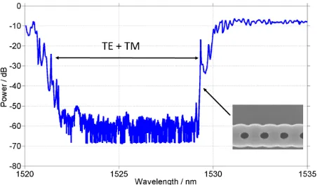
The characterisation of the individual filters, was followed by the measurements of devices combining both filters on the same waveguide. Figures8shows the optical spectra for a TE polarised input signal for a 670µm-long device combining both
improves to a value of approximately 60 dB, which is a value limited by the substrate scattering. When the two coupling coefficients are matched, the same high ER is observed for all the stop band as figure9shows. Similar figures in terms of maximum ER were measured when a TM polarised input beam was coupled to the device. It is worth noting that, although challenging, the 160 nm diameter of the top waveguide holes can be fabricated by DUV lithography [19].
Fig. 8.The experimental transmission optical spectra of the combined sidewall and top grating with 40 nm radius for a TE polarised input signal. An increase of the ER is recorded in the spectral region where both TE and TM stopbands overlap (labelled ‘TE+TM’ in the figure).
Fig. 9.The experimental transmission optical spectra of the combined sidewall and top grating with 80 nm radius for a TE polarised input signal. Because the width of the TM stopband is larger than that of the TE, the benefit produced by filtering the TM mode is visible over the whole stopband.
In this work, silicon waveguide sidewall and top Bragg grat-ing filters were designed, fabricated and characterised as a func-tion of their geometrical parameters. Because of the very dif-ferent modal profile in single mode silicon waveguides, the sidewall geometry is mostly effective on the TE polarised mode while the top grating mostly interacts with the TM polarised mode. Combining these two geometries on the same waveguide allows the design of gratings that are effective on both polarisa-tions thus substantially improving the grating ER. Experimental data show that the ER increases from 30 dB, a limit given by the combination of polarisation scattering inside the waveguide and non-ideal input polarisers, to approximately 60 dB. Such grating geometries also offer a solution for independent polarisation
manipulation on-chip.
Funding:EU under the FP-7 BBOI project (323734) and the EPSRC under the Cornerstone project (EP/L021129/1); G.C. and C.K. acknowledge Fraunhofer Centre for Applied Photonics and EPSRC for the PhD scholarship funding respectively.
The authors wish to thank the staff of the James Watt Nanofab-rication Centre at the University of Glasgow.
REFERENCES
1. D. T. H. Tan, K. Ikeda, R. E. Saperstein, B. Slutsky, and Y. Fainman, Opt. Lett.33, 3013 (2008).
2. M. J. Collins, C. Xiong, I. H. Rey, T. D. Vo, J. He, S. Shahnia, C. Rear-don, T. F. Krauss, M. J. Steel, a. S. Clark, and B. J. Eggleton, Nature communications4, 2582 (2013).
3. S. Azzini, D. Grassani, M. J. Strain, M. Sorel, L. G. Helt, J. E. Sipe, M. Liscidini, M. Galli, and D. Bajoni, Opt. Express20, 23100 (2012). 4. Y. de Koninck, F. Raineri, A. Bazin, R. Raj, G. Roelkens, and R. Baets,
Opt. Lett.38, 2496 (2013).
5. S. Keyvaninia, G. Roelkens, D. V. Thourhout, C. Jany, M. Lamponi, A. L. Liepvre, F. Lelarge, D. Make, G.-H. Duan, D. Bordel, and J.-M. Fedeli, Opt. Express21, 3784 (2013).
6. C. Sima, J. C. Gates, H. L. Rogers, B. D. Snow, C. Holmes, M. N. Zervas, and P. G. R. Smith, Journal of Physics: Conference Series276, 012089 (2011).
7. L. M. Rivas, M. J. Strain, D. Duchesne, A. Carballar, M. Sorel, R. Moran-dotti, and J. A. na, Opt. Lett.33, 2425 (2008).
8. A. M. Prabhu, A. Tsay, Z. Han, and V. Van, IEEE Photonics Journal2, 436 (2010).
9. F. Morichetti, A. Canciamilla, C. Ferrari, M. Torregiani, A. Melloni, and M. Martinelli, Phys. Rev. Lett.104, 033902 (2010).
10. X. Wang, W. Shi, R. Vafaei, N. A. F. Jaeger, and L. Chrostowski, IEEE Photonics Technology Letters23, 290 (2011).
11. M. J. Strain and M. Sorel, IEEE Journal of Quantum Electronics46, 774 (2010).
12. M. Yamada and K. Sakuda, Applied optics26, 3474 (1987).
13. J. R. Ong, R. Kumar, and S. Mookherjea, IEEE Photonics Technology Letters25, 1543 (2013).
14. J. R. Ong, R. Kumar, and S. Mookherjea, Opt. Lett.39, 4439 (2014). 15. N. C. Harris, D. Grassani, A. Simbula, M. Pant, M. Galli, T. Baehr-Jones,
M. Hochberg, D. Englund, D. Bajoni, and C. Galland, Phys. Rev. X4, 041047 (2014).
16. Lumerical, “Lumerical Mode Solutions,” https://www.lumerical.com/tcad-products/mode/.
17. D. F. G. Gallagher and T. P. Felici, Proceedings of SPIE4987, 69 (2003).
18. M. J. Strain, S. Thoms, D. S. MacIntyre, and M. Sorel, Opt. Lett.39, 413 (2014).
[image:4.612.58.286.382.514.2]FULL REFERENCES
1. D. T. H. Tan, K. Ikeda, R. E. Saperstein, B. Slutsky, and Y. Fainman, “Chip-scale dispersion engineering using chirped vertical gratings,” Opt.
Lett.33, 3013–3015 (2008).
2. M. J. Collins, C. Xiong, I. H. Rey, T. D. Vo, J. He, S. Shahnia, C. Reardon, T. F. Krauss, M. J. Steel, a. S. Clark, and B. J. Eggleton, “Integrated spatial multiplexing of heralded single-photon sources.” Nature com-munications4, 2582 (2013).
3. S. Azzini, D. Grassani, M. J. Strain, M. Sorel, L. G. Helt, J. E. Sipe, M. Liscidini, M. Galli, and D. Bajoni, “Ultra-low power generation of twin photons in a compact silicon ring resonator,” Opt. Express20, 23100–23107 (2012).
4. Y. de Koninck, F. Raineri, A. Bazin, R. Raj, G. Roelkens, and R. Baets, “Experimental demonstration of a hybrid iii/v-on-silicon microlaser based on resonant grating cavity mirrors,” Opt. Lett.38, 2496–2498 (2013). 5. S. Keyvaninia, G. Roelkens, D. V. Thourhout, C. Jany, M. Lamponi,
A. L. Liepvre, F. Lelarge, D. Make, G.-H. Duan, D. Bordel, and J.-M. Fedeli, “Demonstration of a heterogeneously integrated iii-v/soi single wavelength tunable laser,” Opt. Express21, 3784–3792 (2013). 6. C. Sima, J. C. Gates, H. L. Rogers, B. D. Snow, C. Holmes, M. N.
Zervas, and P. G. R. Smith, “Simple planar bragg grating devices for photonic hilbert transformer,” Journal of Physics: Conference Series
276, 012089 (2011).
7. L. M. Rivas, M. J. Strain, D. Duchesne, A. Carballar, M. Sorel, R. Moran-dotti, and J. A. na, “Picosecond linear optical pulse shapers based on integrated waveguide bragg gratings,” Opt. Lett.33, 2425–2427 (2008). 8. A. M. Prabhu, A. Tsay, Z. Han, and V. Van, “Extreme miniaturization of
silicon add–drop microring filters for vlsi photonics applications,” IEEE Photonics Journal2, 436–444 (2010).
9. F. Morichetti, A. Canciamilla, C. Ferrari, M. Torregiani, A. Melloni, and M. Martinelli, “Roughness induced backscattering in optical silicon waveguides,” Phys. Rev. Lett.104, 033902–033905 (2010).
10. X. Wang, W. Shi, R. Vafaei, N. A. F. Jaeger, and L. Chrostowski, “Uniform and sampled bragg gratings in soi strip waveguides with sidewall corrugations,” IEEE Photonics Technology Letters23, 290– 292 (2011).
11. M. J. Strain and M. Sorel, “Design and fabrication of integrated chirped bragg gratings for on-chip dispersion control,” IEEE Journal of Quantum Electronics46, 774–782 (2010).
12. M. Yamada and K. Sakuda, “Analysis of almost-periodic distributed feedback slab waveguides via a fundamental matrix approach.” Applied optics26, 3474–3478 (1987).
13. J. R. Ong, R. Kumar, and S. Mookherjea, “Ultra-high-contrast and tunable-bandwidth filter using cascaded high-order silicon microring filters,” IEEE Photonics Technology Letters25, 1543–1546 (2013). 14. J. R. Ong, R. Kumar, and S. Mookherjea, “Silicon microring-based
wavelength converter with integrated pump and signal suppression,” Opt. Lett.39, 4439–4441 (2014).
15. N. C. Harris, D. Grassani, A. Simbula, M. Pant, M. Galli, T. Baehr-Jones, M. Hochberg, D. Englund, D. Bajoni, and C. Galland, “Integrated source of spectrally filtered correlated photons for large-scale quantum photonic systems,” Phys. Rev. X4, 041047–041057 (2014).
16. Lumerical, “Lumerical Mode Solutions,” https://www.lumerical.com/tcad-products/mode/.
17. D. F. G. Gallagher and T. P. Felici, “Eigenmode Expansion Methods for Simulation of Optical Propagation in Photonics -Pros and Cons,” Proceedings of SPIE4987, 69–82 (2003).
18. M. J. Strain, S. Thoms, D. S. MacIntyre, and M. Sorel, “Multi-wavelength filters in silicon using superposition sidewall bragg grating devices,” Opt. Lett.39, 413–416 (2014).
![Fig. 1. Simulated optical spectra of sidewall gratings for theTE polarisation on a SOI single-mode waveguide as a functionof (a) the grating length with a fixed grating amplitude of 5nm and (b) grating amplitude with a fixed grating length of 50µm [16]](https://thumb-us.123doks.com/thumbv2/123dok_us/1464886.99141/1.612.332.564.284.549/simulated-sidewall-gratings-polarisation-waveguide-functionof-amplitude-amplitude.webp)
![Fig. 4. Theoretical losses of the (a) TE and (b) TM polarisedmode as a function of the grating hole radius and etchingdepth [16].](https://thumb-us.123doks.com/thumbv2/123dok_us/1464886.99141/2.612.57.289.207.479/fig-theoretical-losses-polarisedmode-function-grating-radius-etchingdepth.webp)
![Fig. 5. The optical spectra of the TM polarisation on a singlemode SOI waveguide with circular top gratings as a func-tion of the (a) grating length with a hole radius of 40 nm anddepth of 40 nm and (b) hole radius with a length of 670 µmand depth of 40 nm [16].](https://thumb-us.123doks.com/thumbv2/123dok_us/1464886.99141/3.612.63.296.54.324/spectra-polarisation-singlemode-waveguide-circular-gratings-grating-anddepth.webp)