Photoluminescence upconversion at GaAs
/
InGaP
2interfaces driven by a sequential two-photon
absorption mechanism
N. P. Hylton,1,*T. F. Hinrichsen,1,2,†A. R. Vaquero-Stainer,1M. Yoshida,1A. Pusch,1M. Hopkinson,3O. Hess,1 C. C. Phillips,1and N. J. Ekins-Daukes1
1Department of Physics, The Blackett Laboratory, Imperial College London, South Kensington Campus, London SW7 2AZ, United Kingdom
2IV. Physikalisches Institut, Georg-August-Universit¨at G¨ottingen, 37077 G¨ottingen, Germany
3Department of Electronic and Electrical Engineering, University of Sheffield, Sheffield S1 3JD, United Kingdom
(Received 29 February 2016; revised manuscript received 14 April 2016; published 9 June 2016)
This paper reports on the results of an investigation into the nature of photoluminescence upconversion at GaAs/InGaP2interfaces. Using a dual-beam excitation experiment, we demonstrate that the upconversion in our sample proceeds via a sequential two-photon optical absorption mechanism. Measurements of photoluminescence and upconversion photoluminescence revealed evidence of the spatial localization of carriers in the InGaP2 material, arising from partial ordering of the InGaP2. We also observed the excitation of a two-dimensional electron gas at the GaAs/InGaP2heterojunction that manifests as a high-energy shoulder in the GaAs photoluminescence spectrum. Furthermore, the results of upconversion photoluminescence excitation spectroscopy demonstrate that the photon energy onset of upconversion luminescence coincides with the energy of the two-dimensional electron gas at the GaAs/InGaP2interface, suggesting that charge accumulation at the interface can play a crucial role in the upconversion process.
DOI:10.1103/PhysRevB.93.235303
I. INTRODUCTION
Photoluminescence (PL) upconversion, the emission of a high-energy photon following the absorption of two or more lower energy photons, has long been known to occur at the interfaces between III-V semiconductors [1–12]. Although it has been observed in a variety of materials, considerable work has been devoted to investigating the phenomenon at the interface of GaAs and InGaP2 layers [1–3,5,10,11].
Nevertheless there is no general consensus in the literature regarding the mechanism by which the upconversion process occurs. Early reports from Driessenet al.[1,2] suggested that a cold Auger process was responsible for the upconversion PL (UPL) signal in their samples. This claim was supported by a collinear beam PL excitation (PLE) spectroscopy experiment, in which the authors observed a step in the two-beam luminescence signal when the excitation energy was tuned through the GaAs band edge. This was interpreted as an indication that both beams contributed to upconversion only by excitation of carriers in the GaAs, thereby increasing the carrier population available to the Auger process (the rate of which was a nonlinear function of carrier density). Meanwhile, other groups working on upconversion in similar GaAs/InGaP2
samples suggested that the mechanism responsible was a two-step (i.e., sequential) absorption process. This assertion was supported by measurements of the upconversion signal when
*Author to whom correspondence should be addressed:
†Present address: Cavendish Laboratory, University of Cambridge, 19 J J Thomson Avenue, Cambridge CB3 0HE, UK.
Published by the American Physical Society under the terms of the
Creative Commons Attribution 3.0 License. Further distribution of this work must maintain attribution to the author(s) and the published article’s title, journal citation, and DOI.
the excitation energy was below that of the GaAs exciton [10], by pressure and magnetic field dependent measurements of the upconversion luminescence [11], and by using time-resolved PL to study the rate of decay of the upconverted PL [3,5]. While there has been no general agreement on the upconversion mechanism, there has similarly been a variety of reports in the literature of the effect of growth and structural parameters on the upconverted luminescence [2,10,11,13], perhaps indicating a level of interdependency that leads to variation in the nature of the upconversion between different samples.
Interest in the phenomenon of PL upconversion has recently been reignited [7,8], in part owing to the recognition of its potential to improve the efficiency of solar cells, either directly [14] or as an internal process within an intermediate band solar cell [15]. However, to usefully take advantage of an upconverting layer such as the GaAs/InGaP2interface, it is
necessary to reliably determine the mechanism by which the upconversion proceeds.
Herein, we therefore present a spectroscopic analysis of upconversion observed in an InGaP2 p-i-nsolar cell grown
on a GaAs substrate. In this paper, we focus purely on optical spectroscopy of the upconverted luminescence to shed light on the mechanism involved, while Barnhamet al.[16] previously reported the electrical properties of the solar cell under normal operation. By using a dual-beam excitation experiment, we demonstrate that the upconversion in our sample proceeds via a sequential two-photon absorption mechanism.
II. EXPERIMENTAL
The InGaP2 p-i-n structure, known as sample M810, was
grown on ann-type (001) GaAs substrate by molecular beam epitaxy (MBE) at the University of Sheffield. First a 250 nm
n-GaAs buffer layer was grown, upon which 300 nm of
n-type InGaP2 was deposited; the doping density for both
FIG. 1. (a) Band edge diagram of M810 calculated using Nextnano3 (see Ref. [19]). 0 nm on the abscissa represents the top surface of the sample. A magnified representation of the band bending in the conduction band at then-type GaAs/InGaP2interface is shown in the inset. The conduction and valence bands are labeled with C.B. and V.B., respectively. (b) Schematic showing the spatial localization of carriers in the InGaP2due to alloy ordering, as well as how upconversion can proceed via sequential two-photon absorption at the rear interface.
undoped InGaP2 was grown next, followed by 150 nm of p-type InGaP2 with a doping density of 1×1018cm−3. The
MBE grown InGaP2 such as this typically exhibits weak
partial ordering [17,18]. Finally, a 10 nm capping layer of p-GaAs with a doping density of 2×1018cm−3 was
deposited.
To enable a better understanding of the optoelectronic processes in sample M810, we performed a calculation of the electronic structure of the sample using the well-established Poisson-Schr¨odinger solver Nextnano3 [19]. Presented in Fig. 1(a) are the calculated conduction and valence band edges from the sample surface to the substrate. There are two GaAs/InGaP2 interfaces where upconversion may occur
and of particular interest is the alignment at these interfaces. The top surface of the sample is to the left of the diagram at 0 nm and shows the first, or front, interface where the 10 nm
p-GaAs cap meets thep-type InGaP2material. At a depth of
1410 nm in the sample, in then-type region, is the second, or rear, GaAs/InGaP2interface at the buffer layer. Due to the
doping levels in the two interface regions of the sample, the conduction and valence bands are pinned such that while we expect a type I interface, the valence band (conduction band) provides the majority of the band offset in then-type (p-type) material.
The Nextnano3 results also depict band bending at both of the GaAs/InGaP2interfaces where the band offsets are pinned
by the Fermi level. In particular, the inset of Fig.1(a)shows in detail the bending in the conduction band in then-type region. However, it is important to note at this stage that Nextnano3 does not account for any residual CuPt ordering of the InGaP2
material, which is known to occur in samples grown under similar conditions [17,18]. It has been shown that partial CuPt ordering of the InGaP2 gives rise to polarization fields and
hence sheet charge at the interfaces with the GaAs, which we expect to further exaggerate the band bending observed at the interfaces [20–22]. This is important because the triangular potential that arises due to this band bending has been reported
to lead to the formation of a two-dimensional electron gas (2DEG) close to the interface [21,22]. This will be discussed in more detail later.
The partial CuPt ordering also acts to reduce the band gap of the InGaP2compared to fully disordered material and
introduces spatially localized states due to local variations in the alloy ordering (and hence the band gap). This is depicted in Fig. 1(b) in which a schematic of the rear interface is presented. The diagram also shows how PL upconversion can proceed via sequential two-photon absorption at the rear interface.
Spectroscopic measurements were performed in a closed-cycle helium cryostat at a temperature of 10–20 K, using a variety of excitation sources appropriate to the measurements. The PL was excited using a pulsed PicoQuant laser diode emitting at 2.583 eV and operated at a repetition rate of 80 MHz. Meanwhile, the excitation source used for detailed measurements of the PL spectrum from the GaAs layers was a Spectra-Physics tuneable, continuous wave (CW) Ti:sapphire laser, pumped by a solid state Millennia V. The luminescence was dispersed by a 0.5 m spectrometer and detected using either a Si photodiode or a cooled GaAs photomultiplier tube using standard lock-in techniques.
In the cases of the UPL, as well as the PLE spectroscopy and upconversion excitation spectroscopy, the excitation source was again the Ti:sapphire laser, operated in the range 1.459– 1.771 eV. Here we additionally used appropriate optical filters to reject stray light and separate sample luminescence from the excitation source. Finally, for the dual-beam PL and excitation spectroscopy, we used a CW diode laser emitting at 1.699 eV in conjunction with the Ti:sapphire, which was tuned from 1.240– 1.771 eV. Once again, appropriate filtering of the excitation and emission beams was employed.
Note that the pulsed laser diode was used only for the high photon energy excitation source in PL measurements of the InGaP2. All of the upconversion spectroscopy was performed
[image:2.608.68.544.69.251.2]FIG. 2. (a) Photoluminescence spectra of sample M810 measured at low temperature with excitation power densities of 5.5 Wcm−2(black curve) and 6.7 m Wcm−2(red dashed curve). (b) InGaP
2 luminescence measured as a function of excitation power density. The spectra are normalized to the intensity of the high energy (1.955 eV) InGaP2luminescence.
III. RESULTS AND DISCUSSION A. PL spectroscopy
To determine the overall emission profile from the sample, PL spectra were measured at different excitation powers. Shown in Fig.2(a)are low temperature PL spectra of sample M810, excited above the InGaP2band edge at a photon energy
of 2.583 eV and at two different time-averaged power densities. At the higher power density of 5.5 Wcm−2 (black curve), we observe a strong PL peak from the InGaP2at 1.955 eV, as well
as a weak, low energy tail extending to 1.90 eV. An additional peak arising from recombination in the GaAs can be seen close to 1.556 eV. At the lower power density (red dashed curve, 6.7 m Wcm−2), the GaAs PL peak remains visible, whereas the InGaP2luminescence can be characterized by two strong,
distinct peaks. The peak at 1.955 eV remains present, but the intensity is lower by a factor of around 3000, revealing PL from the low energy shoulder at 1.920 eV as well as a third peak emerging at 1.873 eV. Additionally we observe an extended low energy tail to the InGaP2peak at this low excitation power
density, with weak luminescence detected until the onset of the GaAs peak.
That the low-energy features in the InGaP2 PL spectra in
Fig.2(a)are observed only at low power density is indicative of a low density of states. This observation was confirmed by measurements of the InGaP2PL as a function of excitation
power density from 2.2 m Wcm−2to 4.3 Wcm−2. The resulting
spectra are shown in Fig.2(b)normalized to the intensity of the high-energy InGaP2 peak. At the lowest power density,
the peak at 1.920 eV dominates the spectrum, being more intense than the high-energy InGaP2peak by a factor of 1.9.
As the power density is increased, however, this low-energy InGaP2 peak quenches with respect to the peak at 1.955 eV
until it is visible only as a weak tail to the PL at the highest power density. We ascribe these observations to the presence of spatially localized states in the InGaP2material that give rise to
the low energy features and become saturated at high excitation power densities. In contrast, the high-energy InGaP2peak in
Fig.2corresponds to delocalized band-to-band recombination.
Further evidence of localization in the InGaP2 was found in
the form of characteristic nonexponential PL decay curves (not shown here) measured using time correlated single photon counting.
This type of spatial localization may be crucial to the upconversion in that it can act as a trap for upconverted carriers and slow their relaxation back into the GaAs, as depicted schematically in Fig.1(b). We also note at this stage that the presence of two peaks in the PL spectra and evidence for a spread of localized tail states in the InGaP2 are commonly
reported for partially ordered material [23–28]. Moreover, the energy of the InGaP2 band-to-band luminescence in sample
M810 is only slightly lower than that reported for fully disordered material and indicates a low degree of partial ordering in this sample [26,29].
A more detailed graph of the GaAs PL is presented in Fig. 3. Here the sample was excited at 1.676 eV with a power density of 560 Wcm−2, comparable to that used in the
upconversion measurements discussed later. To measure the full spectrum, a silicon photodiode was used in the detection
[image:3.608.58.556.68.246.2] [image:3.608.313.559.554.733.2]FIG. 4. Low temperature photoluminescence and upconversion photoluminescence spectra of M810.
system to extend the observable range of photon energies to
<1.1 eV. We observe a broad luminescence peak centered on 1.520 eV, which is consistent with reported emission energies for band edge recombination in bulk n-type GaAs [30,31]. We additionally observe a high-energy shoulder to this peak at about 1.560 eV, which has previously been reported as indicative of the formation of a 2DEG due to polarization fields at the interface between GaAs and InGaP2[21,22] and
corresponds to the region of the sample shown in the inset of Fig.1(a), close to the rear heterojunction. At lower energies, we observe a luminescence band centered on 1.214 eV, which is a common feature in n-type GaAs and can be ascribed to donor-acceptor type transitions where the acceptor level is formed by a Ga vacancy [32–34]. Since this luminescence band is associated withn-type material, we expect it to originate from the buffer layer and/or the substrate in our sample.
B. UPL measurements
Having observed evidence of partial ordering and the spatial localization of carriers in the normal InGaP2PL, as well as an
interface feature in the GaAs luminescence, we next turn our attention to UPL. In this case the laser was tuned to a photon energy of 1.720 eV, i.e., below the InGaP2band edge, such that
absorption occurs in the GaAs only. The resulting PL and UPL spectra are plotted together in Fig.4. In addition to the strong PL at the GaAs band edge we observe a broad luminescence peak at energies higher than the excitation, which we attribute to recombination of upconverted carriers in the InGaP2. This
peak is centered at 1.918 eV and appears to be a combination of the two InGaP2peaks observed in the normal PL experiments.
The InGaP2 upconversion luminescence is considerably
weaker than the GaAs PL, with its peak intensity roughly 0.022% of the GaAs. This upconversion ratio is lower than that observed by other groups [5,10] and is most likely a result of the position of the GaAs/InGaP2 interfaces in the
sample structure. As described in Sec.II, there are two possible interfaces where the upconversion process can occur. The first is near the top of the sample, where thep-type InGaP2meets
thep-type GaAs capping layer. Since the GaAs cap is merely 10 nm thick, only a small fraction (roughly 2% given an
reabsorbed, given an absorption coefficient of 1×104cm−1
for InGaP2at a photon energy of 1.92 eV [36].
C. Excitation spectroscopy of the GaAs PL and InGaP2UPL
In order to better understand the mechanisms responsible for the upconversion process, we performed a series of exci-tation spectroscopy experiments, studying the PLE spectra for both the GaAs PL and the InGaP2UPL. In the graphs of PLE
and UPLE, we have corrected the signal intensity to account for variations in output power of the Ti:sapphire laser at the extremes of its tuning range. However, the resulting caveat for the UPLE spectra is that the UPL signal is known to be nonlinear with excitation power density [1,6,10]. We therefore concern ourselves primarily with trends in the data rather than absolute figures. Shown in Fig.5(a)are the excitation spectra for the GaAs PL, measured at three different detection energies across the peak of the GaAs luminescence. When measuring on the low energy side of the GaAs PL (at 1.476 eV, black curve), we observe a peak in the excitation spectrum close to the GaAs band edge at 1.547 eV, which is most likely related to the excitation of excitons in the GaAs. The peak exhibits a Burstein-Moss shift and appears broad, as reported elsewhere for GaAs/InGaP2 samples that exhibit partial ordering of the
InGaP2 layer and charge accumulation in the GaAs near the
heterointerface [21,37]. At higher excitation energies (above
∼1.68 eV), we observe a quenching of the GaAs PL intensity that is common to all three detection energies across the GaAs PL and that is consistent with interface recombination loss. At these higher excitation energies, the rising [35] absorption coefficient of GaAs means that carrier generation occurs predominantly at the interface thereby increasing the effect of nonradiative interface recombination.
As an aside, we note also that the form of the PLE spectrum when detecting at 1.560 eV (blue curve) is different to those detected at 1.476 and 1.521 eV. The detection energy in this case coincides with the high energy shoulder of the GaAs luminescence that arises from the excitation of a 2DEG at the GaAs/InGaP2interface. At excitation energies from 1.610 to
FIG. 5. Excitation spectra of (a) the GaAs PL and (b) the InGaP UPL. The excitation spectra were measured at different energies across the GaAs and InGaP2peaks as shown in the respective insets. The PLE curves have been corrected for the intensity of the laser as a function of its emission energy.
penetration depth of the laser at these photon energies means that a greater fraction of incident photons are absorbed close to the interface. Hence we observe increasing PL signal with increasing excitation energy until the effect is overcome by the interface losses noted above.
Consider now the InGaP2UPLE spectra plotted in Fig.5(b).
In contrast with some earlier reports [1,38], the onset of the InGaP2 UPL in our sample occurs at around 1.560 eV, again
concurrent with thehighenergy shoulder of the GaAs PL peak and the anticipated excitation of the 2DEG. Below this photon energy, no UPL signal was recorded. We therefore infer that the 2DEG present at the interface has a role to play in the upconversion process.
As the excitation photon energy is increased further, the UPL intensity in Fig.5(b)rises to a plateau at around 1.670 eV and then rises sharply above 1.7 eV. This can be explained by the rising absorption coefficient for GaAs with increasing photon energy, which means that more carriers are generated in the region of GaAs close to the interface with the InGaP2
and can contribute to the upconversion signal. Additionally, we also note that this increase in signal at high photon energies is inversely correlated (though at a different order of magnitude) with the quenching of the PLE intensity when detecting on the GaAs peak, as shown by the normalized plots in Fig.6. This inverse correlationmaytherefore be an indicator that the upconversion occurs predominantly at the rear interface.
We also note from Fig.5(b)that for excitation energies in the range 1.58–1.70 eV, the InGaP2 luminescence detected at
1.938 eV exhibits the greatest intensity, while at excitation energies above 1.70 eV the InGaP2 luminescence detected
at 1.920 eV dominates. To explore this phenomenon further, we measured the UPL spectrum at several excitation energies spanning the range of this cross-over. The resulting spectra are plotted in Fig.7(a)and demonstrate that as the excitation energy is reduced from 1.744 to 1.590 eV, the UPL peak blue-shifts by around 22 meV. We also observe a change in the shape of the UPL spectrum as the excitation energy changes. Recall from the earlier discussion of Fig.4 that the UPL spectrum appears to consist of the two peaks (due to spatially localized
states and band-to-band recombination) that were observed in the InGaP2PL. It is now clear from Fig.7(a)that the relative
contribution of the peaks in the UPL changes depending upon the excitation energy.
In Fig.7(b)is shown a plot of the PL spectrum excited at 2.583 eV as well as two of the UPL curves from Fig.7(a), all normalized to their maximum intensity. We observe that at an excitation energy of 1.744 eV, the low energy peak (arising from the recombination of carriers that are spatially localized by partial ordering in the InGaP2) dominates the
UPL spectrum, while at an excitation energy of 1.610 eV the band-to-band recombination takes over, hence the cross-over in the InGaP2 UPLE spectra from Fig. 5(b). This behavior
indicates that the upconverted carriers are captured into a subset of the spread of spatially localized states in the InGaP2 that is dependent upon the excitation energy. As the
rear GaAs/InGaP2 interface represents the beginning of the
InGaP2 growth it is reasonable to assume that the spread of
localized states may vary in the direction of growth as a result of the change in growth conditions. One possible explanation
[image:5.608.312.560.547.723.2]FIG. 7. Upconversion PL spectra measured as a function of excitation energy (a). UPL spectra measured at excitation energies of 1.744 and 1.610 eV compared with normal InGaP2PL excited at 2.583 eV (b).
therefore is that more energetic upconverted carriers (generated at higher excitation energies) may diffuse further into the InGaP2, thus accessing a differing subset of localized
states and hence shifting the peak of the UPL spectrum.
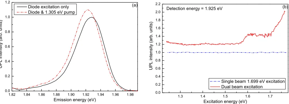
D. Dual-beam UPL and excitation spectroscopy Finally we carried out a dual-beam experiment designed to enable the determination of the mechanism by which upconversion proceeds in sample M810. We chose one beam to be of fixed energy, provided by a diode laser emitting at 1.699 eV, while the second auxiliary beam was tuneable in order to probe the effects of excitation across the GaAs band edge. In this experiment only the diode laser was chopped and used for the lock-in detection, meaning that the tuneable auxiliary beam could provide only an additional upconversion signal when both beams were present and not a separate upconversion PL signal. The solid curve in Fig.8(a)shows the PL spectrum recorded without the tuneable auxiliary beam, i.e., a standard upconversion PL spectrum. This is shown for comparison with the red curve measured when the two beams were coincident at the same spot on the sample. In this case the tuneable laser was set to a photon energy of 1.305 eV,belowthe GaAs band edge. The difference between the two upconversion PL spectra demonstrate that the unchopped beam provided additional UPL signal, with a peak intensity roughly 10% higher than that from the diode laser alone. We note that for the dual-beam excitation, the UPL peak was red shifted slightly (∼5 meV). This effect is most likely due to local heating of the sample arising from the additional laser excitation and fits with a small (∼10 K) rise in temperature [39].
The results of the dual-beam excitation spectroscopy are plotted in Fig.8(b), where the blue line shows the baseline, i.e., the UPL signal when only the fixed photon energy diode laser is present. The red curve shows the excitation spectrum measured when both beams were incident on the sample and clearly demonstrates that an additional upconversion signal was observed for all photon energies in the range of the Ti:sapphire laser from 1.240–1.771 eV.
To further explain this result, we first consider the excitation energy range above the high-energy shoulder in the GaAs PL at 1.560 eV. At these high photon energies, we observe an increase in the UPL signal of between 20 and 40%, compared to single beam excitation. We stress that this increase is not related to any shift of the PL due to sample heating. Indeed the PL red shift arising from local heating of the sample would act to reduce the recorded intensity in the dual-beam PLE experiment since the detection energy would no longer be at the peak of the UPL. At even higher excitation energies (above ∼1.7 eV), we observe a steep rise in the additional UPL signal, which correlates well with our observation of an increase in the single beam UPLE in Fig.5(b). In the part of the spectrum where the photon energy of the tuneable auxiliary beam was below 1.560 eV, we still observe additional UPL of around 20%. Crucially, this additional UPL signal persists well below the GaAs band edge. This is a key step towards understanding the upconversion mechanism in our sample; if Auger recombination was driving the upconversion process, then the second beam would only be able to provide additional upconverted light by generating additional carriers in the GaAs, i.e., at excitation photon energies above the GaAs band edge or by a small boost to the efficiency of the Auger process via local heating. Since considerable additional upconversion was observed below the energetic threshold presented by the GaAs band edge and due to the flat spectral nature of the additional upconversion signal, we conclude that a sequential absorption process is responsible. In the sequential absorption case, additional upconversion could, in principle, be observed for all photon energies higher than the ∼500 meV band offset between GaAs and InGaP2, although that is beyond
FIG. 8. Dual-beam upconversion photoluminescence (a) and excitation spectra (b) shown with and without the second pump beam. The detection energy in (b) was 1.925 eV, and the dual-beam curve has been corrected for the variation in laser intensity across its tuning range, as for the previous PLE plots.
throughout the buffer layer and substrate, not located in high density near the interface with InGaP2.
IV. CONCLUSIONS
We have demonstrated sequential two-photon absorption mediated UPL in ap-i-nInGaP2structure grown on GaAs. Via
a dual-beam experiment, we showed that sequential absorption is responsible for the upconversion mechanism in our sample since the additional upconversion from the auxiliary beam was detected even at excitation energies below the GaAs band gap. We observed evidence of spatial localization in the InGaP2
material in the form of distinct PL peaks in the luminescence experiments that merge into a single broad peak in the UPL. The relative contribution of these peaks to the UPL was also shown to be dependent upon the excitation energy. Excitation spectroscopy performed on the InGaP2UPL demonstrated that
in our sample the UPL signal appears not at the GaAs band edge but rather at the higher energy side of the GaAs PL. This is coincident with an interface 2DEG feature in the GaAs PL, highlighting the importance of charge accumulation at the interface. Comparing the form of the GaAs PLE and the InGaP2 UPLE also revealed an inverse correlation at photon
energies between 1.56 and 1.76 eV. Since the quenching observed in the GaAs PLE arises from increasing interface recombination at high excitation energies, the corresponding increase in the UPLE is an indication that the upconversion occurs predominantly at the rear heterointerface in this sample.
Our results shed new light on upconversion processes in inorganic semiconductors and may represent a step towards harnessing this phenomenon for application in optoelectronic devices. In particular, this type of PL upconversion could, in principle, be harnessed in solar cells, enabling absorption and hence a photocurrent from a greater portion of the solar spectrum, while maintaining an open circuit voltage derived from wider band gap material.
ACKNOWLEDGMENTS
The work described in this paper was conducted with the financial support of the Engineering and Physical Sciences Research Council under Grant No. EP/K029398/1. T.F.H. would like to thank Prof. Angela Rizzi for supporting his placement at Imperial College London and for helpful discussions.
NED conceived the idea of the paper, and N.P.H., T.F.H. and A.R.V.S. planned and conducted the experiments. All authors contributed to the analysis of the results. N.P.H. wrote the manuscript, and all authors reviewed and contributed to the final version.
Data used in the graphs presented in this paper may be provided upon request. Please contact the Experimental Solid State group in the Physics Department of Imperial College London at the following email address: [email protected].
N.P.H. and T.F.H. contributed equally to this work.
[1] F. A. J. M. Driessen, Appl. Phys. Lett. 67, 2813
(1995).
[2] F. Driessen, H. Cheong, A. Mascarenhas, S. Deb, P. Hageman, G. Bauhuis, and L. Giling,Phys. Rev. B Condens. Matter54,
R5263(1996).
[3] T. Kita, T. Nishino, C. Geng, F. Scholz, and H. Schweizer,J. Lumin.87-89,269(2000).
[4] K. Yamashita, T. Kita, and T. Nishino,J. Appl. Phys.84,359
(1998).
[5] T. Kita, T. Nishino, C. Geng, F. Scholz, and H. Schweizer,Phys. Rev. B59,15358(1999).
[6] K. Yamashita, T. Kita, T. Nishino, and M. Oestreich, Jpn. J. Appl. Phys.38,1001(1999).
A. Pusch, O. Hess, C. C. Phillips, D. J. Farrell, K. Yoshida, N. Ahsan, Y. Shoji, T. Sogabe, and J.-F. Guillemoles,Appl. Phys. Rev.2,021302(2015).
[16] K. Barnham, J. Connolly, P. Griffin, G. Haarpaintner, J. Nelson, E. Tsui, A. Zachariou, J. Osborne, C. Button, G. Hill, M. Hopkinson, M. Pate, J. Roberts, and T. Foxon,J. Appl. Phys. 80,1201(1996).
[17] D. J. Mowbray, O. P. Kowalski, M. S. Skolnick, M. C. DeLong, M. Hopkinson, J. P. R. David, and A. G. Cullis,J. Appl. Phys. 75,2029(1994).
[18] M. C. DeLong, D. J. Mowbray, R. A. Hogg, M. S. Skolnick, M. Hopkinson, J. P. R. David, P. C. Taylor, S. R. Kurtz, and J. M. Olson,J. Appl. Phys.73,5163(1993).
[19] S. Birner, T. Zibold, T. Andlauer, T. Kubis, M. Sabathil, A. Trellakis, and P. Vogl,IEEE Trans. Electron Devices54,2137
(2007).
[20] P. Krispin, A. Knauer, and S. Gramlich,Appl. Phys. Lett.80,
2493(2002).
[21] K. Yamashita, T. Kita, Y. Matsuura, O. Wada, C. Geng, F. Scholz, H. Schweizer, and K. Oe, Phys. Rev. B66, 195317
(2002).
J. M. Olson,Phys. Rev. B68,035310(2003).
[29] Y. Zhang, A. Mascarenhas, and L.-W. Wang,Phys. Rev. B63,
201312(2001).
[30] G. Borghs, K. Bhattacharyya, K. Deneffe, P. Van Mieghem, and R. Mertens,J. Appl. Phys.66,4381(1989).
[31] I. Vurgaftman, J. R. Meyer, and L. R. Ram-Mohan,J. Appl. Phys.89,5815(2001).
[32] E. W. Williams,Phys. Rev.168,922(1968).
[33] M. Holtz, T. Sauncy, T. Dallas, and S. Massie,Phys. Rev. B50,
14706(R)(1994).
[34] C. J. Hwang,J. Appl. Phys.40,4584(1969). [35] M. D. Sturge,Phys. Rev.127,768(1962).
[36] M. Moser, C. Geng, E. Lach, I. Queisser, F. Scholz, H. Schweizer, and A. D¨ornen,J. Cryst. Growth124,333(1992). [37] K. Yamashita, O. E. Kunishige, T. Kita, O. Wada, Y. Wang, C.
Geng, F. Scholz, and H. Schweizer,Japanese J. Appl. Physics, Part 1 Regul. Pap. Short Notes Rev. Pap.44,7390(2005). [38] M. Izadifard, J. P. Bergman, W. M. Chen, I. A. Buyanova, Y. G.
Hong, and C. W. Tu,J. Appl. Phys.99,073515(2006). [39] M. Kondow, S. Minagawa, Y. Inoue, T. Nishino, and Y.
![FIG. 1. (a) Band edge diagram of M810 calculated using Nextnano3 (see Ref. []). 0 nm on the abscissa represents the top surface of theThe conduction and valence bands are labeled with C.B](https://thumb-us.123doks.com/thumbv2/123dok_us/7850205.178128/2.608.68.544.69.251/diagram-calculated-nextnano-abscissa-represents-conduction-valence-labeled.webp)