1
A Sub k
BT/q Semimetal Nanowire Field Effect Transistor
L. Ansari, G. Fagas, F. Gity, and J. C. Greer
1Tyndall National Institute, Lee Maltings, Dyke Parade, Cork, T12 R5CP, Ireland
The key challenges for nanoelectronics technologies is to identify designs that work on molecular length scales, provide reduced power consumption relative to classical field effect transistors (FETs), and that can be readily integrated at low cost. To this end, a FET is introduced that relies on quantum effects arising for semimetals patterned with critical dimensions below 5 nm, that intrinsically has lower power requirements due to its better than a ‘Boltzmann tyranny’ limited subthreshold swing (SS) relative to classical field effect devices, eliminates the need to form heterojunctions, and mitigates against the requirement for abrupt doping profiles in the formation of nanowire tunnel FETs. This is achieved through using a nanowire comprised of a single semimetal material while providing the equivalent of a heterojunction structure based on shape engineering to avail of the quantum confinement induced semimetal-to-semiconductor transition. Ab initio calculations
combined with a non-equilibrium Green’s function formalism for charge transport reveals tunneling behavior in the OFF state and a resonant conduction mechanism for the ON state. A common limitation to TFET designs is related to a low current in the ON state. A discussion relating the semimetal FET (SM-TFET) design to overcoming this limitation while providing less than 60 meV/dec SS at room temperature is provided.
Increasing manufacturing costs and a lessening cadence for improved performance with new technology nodes is leading to a critical point in the manufacture of advanced nanoelectronics1. For some time, device scaling has failed to provide increased
switching speeds for transistors leading to circuit architectures that rely on increasing the level of parallel processing rather than increasing the amount of processing achievable by a single processor. As transistors are manufactured with 10 nm and 7 nm critical dimensions, source-drain tunneling makes it increasingly difficult to turn devices OFF resulting in higher power considerations for modern circuits manufactured with billions of transistors. Just as increased gate tunneling lead to the introduction of ‘high κ’ dielectrics, continued scaling is leading to the introduction of multi-gate transistor architectures and a search for devices that can overcome the ‘Boltzmann tyranny’ that is inherent in classical field effect transistor (FET) operation.
The subthreshold swing (SS) is a measure of the electrostatic gate control over the drain-source current (IDS) in a
metal-oxide-semiconductor FET (MOSFET). The gate is used to lower the electrostatic barrier between drain and source, the amount of charge carriers able to surmount this barrier is related to the Fermi-Dirac distribution in the source region which for normal operating temperatures can be approximated as a Maxwell-Boltzmann distribution. For fixed temperature, the current IDS
varies exponentially with the gate voltage below the threshold for the transition to the ON-state. For a classical field effect transistor, the thermal emission of carriers over the barrier leads to a theoretical lower limit of approximately 60 mV/decade
2
at room temperature for the SS. This is equivalent to stating that an order of magnitude change of IDS in the subthreshold
region requires approximately a 60 mV change in gate voltage. This thermal lower limit gives rise to the description ‘Boltzmann’s tyranny’ resulting from both Fermi-Dirac statistics and the density of states (DoS) for the charge carriers.
To overcome the thermally limited SS in classical FETs, transistors relying on band-to-band tunneling (BTBT) or tunnel FETs (TFETs) have been introduced2,3. These devices rely on tunneling across a band gap by carriers in the
valence/conduction band edge in the source to a conduction/valence band edge in the drain. Since the carriers are modulated by a gate voltage that brings the tunneling carriers in or out of resonance, the Boltzmann limit does not apply and SS values of 30 to 50 mV/decade have been predicted4. To fabricate a TFET structure, it is often desirable to introduce heterojunctions
to improve performance5,6. However, constructing nanoscale TFETs using heterojunctions and abrupt doping profiles to
define both source and drain can cause large device-to-device variations.
Here a semimetal nanowire field effect transistor (SM-TFET) with lower than the thermal limit for the SS is proposed and advantages related to fabrication and improved transistor properties within the scheme are highlighted. For demonstrating the concept, an α-tin nanowire is used as a prototype. It has been shown that the α-tin phase in thin films can be stabilized7-11.
Furthermore, for α-tin nanowires with diameters below approximately 5 nm, a semimetal-to-semiconductor transition leads to a band gap of >100 meV; the energy of the band gap increases rapidly with reduced nanowire cross section12. Based on the
semimetal-to-semiconductor transition, it was shown by ab initio electronic structure and charge transport calculations that
within a single nanowire -with a region wider than the critical dimension for the transition adjoining a narrow section of the wire with cross section dimensions below the critical dimension- that a semimetal-semiconductor junction in a monomaterial can be formed and will behave as a Schottky barrier. It was further demonstrated that using this behavior in a semimetal nanowire, that a Schottky barrier transistor can be designed12. In the current context, the concept of a monomaterial Schottky
barrier diode is applied to demonstrate that properties of nanowire FETs can be significantly enhanced using this concept, but requires altering the architecture with respect to the Schottky barrier transistor12.
For a ‘zero gap’ bulk semimetal such as α-tin, quantum confinement leads to an induced energy gap in a two-dimensional (film) or one-dimensional (nanowire) between the conduction and valence band edges at the Γ-point in the Brillouin zone. The value of the induced gap is controlled by varying the film thickness or cross sectional area of a semimetal nanowire. The proposal for the SM-TFET is to construct a structure with a semimetal (tin) source adjoining a narrower section of the nanowire, the latter is used to create both an intrinsic semiconducting region as the channel and n-type doped region acting as
the drain. A gate-all-around geometry is introduced to achieve electrostatic gating of the channel region to control tunneling in the sub-threshold region. As will be shown in contrast to conventional TFET architectures, the ON current is not limited by tunneling.
The electronic structure computations are performed using density functional theory (DFT). The local-density approximation (LDA) is used for the exchange-correlation potential13. A numerical atomic orbital basis set for the tin and dopant atoms are
defined using optimized orbitals with three orbitals per atomic level, or ‘triple-zeta’ quality14. Note that the underestimation
of the band gap typical of approximate exchange-correlation functionals used for practical DFT calculations implies that the actual quantum confinement effect occurs at larger nanowire diameters than predicted by the DFT/LDA calculations15; for
3
atomistic structure of the SM-TFET is allowed to relax by minimizing the energy with respect to atom positions until the maximum force component per atoms is less than 0.01 eV/Å. The unit-cell along the transport axis of the device are periodic for the energy minimization and the transverse cell dimensions are chosen large enough to neglect the interaction between neighboring nanowires arising from periodic boundary conditions. The effect of n-type antimony (Sb) doping in the drain
region of the narrow tin nanowire section are evaluated for doping concentrations of ND1 = 2.5×1020 cm−3 and ND2 = 8×10²⁰
cm−3. The electronic band structure of the doped Sn nanowire with a 1 nm diameter is compared to an intrinsic Sn nanowire
with the same diameter in Fig. 1. Dopant atoms are introduced onto substitutional sites. The curvature of the first energy subband in the conduction band is similar in Figs. 1(a) and 1(b) for the intrinsic and lower doping, respectively, while there is slight increase in Fig. 1(c) for the curvature at higher doping. This corresponds to almost equal electron effective mass for the intrinsic and lower doped nanowires of me,intrinsic = 0.089m0 and me,ND1 = 0.093 m0, respectively, and a slightly higher
effective mass of me,ND2 = 0.109 m0 at the higher doping concentration. The doped regions are used to define the drain and for
the analysis of the SM-TFET, both doping concentrations are considered.
[image:3.612.186.430.273.460.2]
FIG. 1. Band structure of (a) intrinsic, (b) n-type with doping concentration of ND1=2.5×1020 cm−3, and (c) n-type with doping
concentration of ND2=8×1020 cm−3 for a 1 nm-diameter tin nanowire with a [110] crystallographic orientation. The zero of energy is taken
to be the Fermi energy.
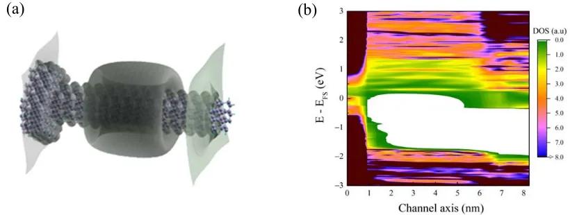
The proposed SM-TFET architecture is shown in Fig. 2. The figure illustrates the atomistic structure of a nanowire with a thicker, approximately square, region of cross sectional area 4.5 nm × 4.5 nm forming the source, and the narrower, approximately circular cross sectional area, with a diameter of 1 nm extending from the wider source region. A physical gate length of 3 nm is shown as the cylindrical equipotential surface wrapped around the channel. There are 1 nm extensions on either side of the gated channel region. The oxide isolating the gate electrode from the channel is treated only through electrostatic coupling, the gate dielectric coupling is chosen to be described by a 1 nm-thick hafnium oxide with a dielectric constant of κHfO2 ~ 25.
4
drain-source bias, there remains an approximately 5 nm long tunneling path and current is strongly suppressed in the OFF state; see fig. 3(a).
FIG. 2. (a) Atomic scale illustration of the proposed SM-TFET structure. All surface dangling bonds are passivated by bonding to hydrogen. (b) The local density of states (LDoS) for the nanowire device in (a). The semimetallic source region is on the left and the zero of energy is taken to be the Fermi level at zero drain-source voltage (VDS) and zero gate voltage (VGS). The central region in white indicates
the band gap for the intrinsic channel, and the region in the right of LDoS diagram indicates the n-type doped drain region also with the band gap indicated in white. Note the formation of MIGS in the lower left and upper right regions in the channel band gap at the source/drain interfaces.
To investigate device operation as drain-source and gate voltage biases are applied, the electron transmission at a given bias point is calculated self-consistently using the DFT/LDA Hamiltonian with self-energies describing ‘semi-infinite’ drain and source electrodes within the method of the non-equilibrium Green’s function (NEGF)16. The 5 nm channel region is
sufficiently large to eliminate coupling between the source and drain, enabling the source/drain regions to be extended as (semi-infinite) ‘ideal’ electrodes. The electrode conditions are achieved by holding the source and drain regions at thermal equilibrium described by Fermi-Dirac distributions at T=300K, but driven away from equilibrium with respect to each other by the chemical potential difference V .
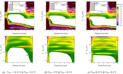
The local density of state (LDoS) across the SM-TFET is plotted in Fig. 3 as a function of energy and position at a fixed drain-source voltage of VDS= +0.3 V and for VGS= 0.12 V (OFF); VGS= 0 (subthreshold region); and VGS= +0.12 V (ON). At
VGS = 0.12 V, the potential profile across the channel leads to the formation of a sharply defined state above the potential
barrier. This state can as a first approximation be thought of as an energy level in a triangular barrier formed between the source/channel barrier, the ‘linear’ voltage drop due to application of VDS across the channel, and the heavily doped drain. In
the OFF state, the tunneling current dominates. As the gate voltage is increased to turn the device ON, the energy level formed in the channel lowers in energy as the potential in the channel lowers and extends further into the channel becoming resonant with occupied states in the source; a side by side comparison between the LDoS in fig. 3 and the energy resolved currents shown in fig. 4 is shown in the Supplementary Material. As the state extends further into the channel at higher gate voltages, it hybridizes with the states in the source (see Fig. 3 (b) and (c) in particular). At sufficiently large gate voltages the channel is effectively in inversion as the state lowers and the source/channel barrier lowers; see fig. 3 (c). In the ON state, higher states formed in the channel begin to couple to thermally excited states in the source and the energy-resolved current is broadened. The voltage barrier as the source ‘collapses’ and electrons near in energy to the source Fermi level can flow
[image:4.612.103.513.102.257.2]5
across the channel region without tunneling. Hence in the ON state the current becomes a combination of tunneling and ‘over the barrier’ transport resulting in a sharp current increase defeating the Boltzmann tyranny limit. The sharply peaked density of states associated with the formation of channel states overcomes the usual assumptions leading to the thermal limit, thereby allowing for a SS < 60 meV/dec.
[image:5.612.76.546.134.417.2]
(a) VGS = −0.12 V & VDS = 0.3 V (b) VGS = 0 V & VDS = 0.3 V (c) VGS=0.12 V & VDS =0.3 V
FIG. 3. Energy resolved local density (LDoS) with VDS=0.3 V and varying VGS for the device with drain doping ND1. (a) OFF-state:
VGS = −0.12 V (b) Sub-threshold region: VGS = 0 V (c) ON-state: VGS = 0.12 V. Similar profiles have been observed with drain
doping ND2. Voltages referenced to the source. A schematic illustration of the band diagram is provided as an inset at each bias point.
Bottom row is an enlarged view of the LDoS for energies near the source Fermi level.
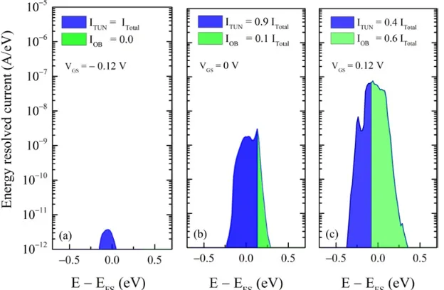
To reinforce the analysis accompanying Fig. 3, the currents from drain to source are decomposed into two components. The first component is the fraction of electrons tunneling across the channel, i.e. for electrons that flow from the source-to-drain
but that are lower in energy than the energy barrier EB at the source-channel interface. The tunneling current from these
electrons is defined as where is the energy resolved current. The second component accounts for
electrons emitted from the source with energies greater than EB or ‘over the barrier’ (OB), their associated current is defined as . Energy resolved current profiles for the bias-dependent contribution of each of the current components
are shown in Fig. 4. For the OFF-state given by VGS = −0.12 V, all electrons tunneling from the source are ‘under the barrier’
and the only current transport is BTBT. As the gate voltage increases to VGS= 0, the energy barrier decreases leading to a
6
Finally as the gate voltage is increased further to VGS= +0.12 V, the majority of the current is due to the ‘over the barrier’
component, but nonetheless the BTBT component remains significant.
[image:6.612.153.465.104.308.2]FIG. 4. Energy-resolved current profiles at (a) VGS = −0.12 V, (b) VGS = 0 V, and (c) VGS = +0.12 V. All currents obtained at VDS = +0.3 V.
The contribution of the tunneling current (area shaded in blue; dark grey in b/w) and over the barrier transport (area shaded in green; light grey in b/w) are shown. Note the position of the potential barrier for VGS= -0.12 V is above the source Fermi level but ‘collapses’ as the
gate voltage is increased. The barrier collapse implies the surface dipole at the source-channel interface can be compensated with increasing gate voltage.
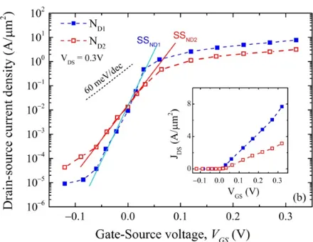
The current-voltage characteristic for the TFET at fixed VDS and varying VGS is shown in fig. 5. Subthreshold swings of 39
mV/dec and 28 mV/dec are predicted with ND1 and ND2 doping concentrations in the drain, respectively, at room temperature.
Thus the tunneling current below threshold dominates and a value for the SS below the theoretical limit of a classical FET is achievable with the design. That is in itself of interest, however other designs offer similar theoretical behavior. However, there are key distinctions between the SM-TFET and previous TFET proposals. The SM-TFET is comprised of a single nanowire that has been thinned in one region, and high performance is achieved without requiring hetero-epitaxy. The fact that the source-channel junction is achieved by shape engineering to generate a Schottky barrier implies no dopant diffusion occurs at the source-channel junction, helping to define a sharp tunneling region. The proposed structure for the SM-TFET provides remarkably higher on-state current in comparison to state-of-the-art TFET designs due to the ‘barrier collape’ and the significant contribution of resonant current6, 17-19 arising from states formed in the channel yielding a sharp peak in the
density of states as the device turns ON. For the drain doping concentration ND1 and ND2, the ON-state at VDS = +0.3 V and
7
FIG. 5. IDS versusVGS characteristics of the SM-TFET for two doping profiles at VDS = 0.3 V. A sub-threshold slope lower than the
‘Boltzmann tyranny’ limit has been achieved at both drain doping concentrations. The inset shows the same plot in linear scale.
It has previously been shown that using heterojunctions in TFET devices improves the device performance6,20,21; however,
constructing TFETs with heterojunctions on nanoscale lengths imposes critical challenges from a device fabrication point of view. Clearly fabrication of the semimetal device poses different challenges in terms of changing the diameter of a nanowire in selected regions and doping of semimetals. Nonetheless, the proposed SM-TFET is constructed from a single material yet is able to introduce a heterojunction at the source-channel junction. Applying the gate electric field modifies the channel band structure allowing for a sharply peak DoS allowing for a much more rapid increase in channel current with gate voltage than associated with conventional FETs.
In summary, a SM-TFET with a heterojunction structure is proposed with a monomaterial design. NEGF simulations reveal
that the proposed SM-TFET architecture provides a remarkably high ON-current due a combination of resonant transport and due to the energy barrier collapse at the source, an effect not seen in semiconductor heterojunctions; see the discussion in Supplementary Material. The barrier collapse and the sharp density of states arising from the resonant state forming in the channel from the drain enables a sharply increasing transmission in the sub-threshold region, and the advantage over conventional TFETs of ‘over the barrier’ transport in the ON-state. The current-voltage characteristics for the SM-TFET indicate that subthreshold slopes lower than the thermal limit for conventional MOSFETs can be achieved with gate lengths of 3 nm and source to drain distance of 5 nm.
SUPPLEMENTARY MATERIAL
8
ACKNOWLEDGMENTS
This research was funded through a Science Foundation Ireland Principal Investigator award 13/IA/1956. The authors would like to acknowledge the SFI/HEA Irish Centre for High-End Computing (ICHEC) for the provision of computational facilities and support.
REFERENCES
1. “Double, double, toil and trouble”, Technology Quarterly, The Economist, March 12 (2016).
2. W. Richardson, J. Coleman and A. Chatterjee, IEEE Electron Device Lett. 8, 347–349 (1987).
3. W. Hansch, C. Fink, J. Schulze, and I. Eisele, Thin Solid Films 369, 387 (2000).
4. R. Gandhi, Z. Chen, N. Singh, K. Banerjee, S. Lee, IEEE Electron Device Lett. 32, 437–739 (2011).
5.
B. Ganjipour, J. Wallentin, M. T. Borgstrom, L. Samuelson, and C. lander,
ACS Nano 6, 3109–3113(2012).
6. K. Tomioka, M. Yoshimura, T. Fukui, Nano Lett. 13, 5822 (2013).
7. W. Paul, J. Appl. Phys. 32, 2082 (1961).
8. B. H. Cheong, K. J. Chang, Phys. Rev. B. 44, 4103 (1991).
9. R. F. C. Farrow, D. S. Robertson, G. M. Williams, A. G. Cullis, G. R. Jones, I. M. Young, P. N. J. Dennis, J. Cryst. Growth 54, 507–518 (1981).
10. P. John, T. Miller, and T.-C. Chiang, Phys. Rev. B 39, 3223 (1989).
11. H. Hochst, I. Hernandez-Calderon, Surf. Sci. 126, 25-31 (1983).
12. L. Ansari, G. Fagas, J. P. Colinge and J. C. Greer, Nano Lett. 12, 2222–2227 (2012).
13. J. P. Perdew, and A. Zunger, Phys. Rev. B 23, 5048 (1981).
14. T. Ozaki, and H. Kino, Phys. Rev. B 69, 195113 (2004).
15. A. Sanchez-Soares, private communication. The increase in the band gap due to quantum confinement for larger nanowire diameters in α-tin is seen with the aid of GW calculations of the direct band gap.
16. T. Ozaki, K. Nishio, H. KinoPhys. Rev. B 81, 035116 (2010).
17. A. M. Ionescu, H. Riel, Nature 479, 329 (2011).
18. R. Kotlyar, U. E. Avci, S. Cea, R. Rios, T. D. Linton, Appl. Phys. Lett. 102, 113106 (2013).
19. S. Datta, H. Liu, V. Narayanan, Microelectronics Reliability 54, 861 (2014).
20. J. Knoch, and J. Appenzeller, IEEE Electron Device Lett. 31, 305 (2010).
![FIG. 1. Band structure of (a) intrinsic, (b) n-type with doping concentration of ND1=2.5×1020 cm−3, and (c) n-type with doping concentration of ND2=8×1020 cm−3 for a 1 nm-diameter tin nanowire with a [110] crystallographic orientation](https://thumb-us.123doks.com/thumbv2/123dok_us/8551800.363028/3.612.186.430.273.460/structure-intrinsic-concentration-concentration-diameter-nanowire-crystallographic-orientation.webp)