Fast and cost-effective in-process defect
inspection for printed electronics based on
coherent optical processing
XIAOBING FENG,
1,4RONG SU,
1,4,*TUOMAS HAPPONEN,
2JIAN LIU,
3AND
RICHARD LEACH
11Manufacturing Metrology Team, Faculty of Engineering, University of Nottingham, Nottingham NG8 1BB, UK
2VTT Technical Research Centre of Finland, P.O. Box 1100, 90571 Oulu, Finland
3Centre of Ultra-Precision Optoelectronic Instrument Engineering, Harbin Institute of Technology, 92 West Da-Zhi Street, Harbin, 150001, China
4Co-first authors with equal contribution *[email protected]
Abstract: This paper presents an all-optical difference engine (AODE) sensor for detecting the defects in printed electronics produced with roll-to-roll processes. The sensor is based on the principle of coherent optical subtraction and is able to achieve high-speed inspection by minimising data post-processing. A self-comparison inspection strategy is introduced to allow defect detection by comparing the printed features and patterns that have the same nominal dimensions. In addition, potential applications of the AODE sensor in an on-the-fly pass-or-reject production control scenario are presented. A prototype AODE sensor using a digital camera is developed and demonstrated by detecting defects on several industrial printed electrical circuitry samples. The camera can be easily replaced by a low-cost photodiode to realise high-speed all-optical information processing and inspection. The developed sensor is capable of inspecting areas of 4 mm width with a resolution of the order of several micrometres, and can be duplicated in parallel to inspect larger areas without significant cost.
Published by The Optical Society under the terms of the Creative Commons Attribution 4.0 License. Further distribution of this work must maintain attribution to the author(s) and the published article’s title, journal citation, and DOI.
OCIS codes: (070.0070) Fourier optics and signal processing; (070.6110) Spatial filtering; (110.0110) Imaging systems; (120.4630) Optical inspection; (280.4788) Optical sensing and sensors.
References and links
1. T. Kololuoma, M. Tuomikoski, T. Mäkelä, J. Heilmann, T. Haring, J. Kallioinen, J. Hagberg, I. Kettunen, and H. Kopola, “Towards roll-to-roll fabrication of electronics, optics and optoelectronics for smart and intelligent packaging,” Proc. SPIE 5363, 77–85 (2004).
2. S. Khan, L. Lorenzelli, and R. S. Dahiya, “Technologies for printing sensors and electronics over large flexible substrates: A review,” IEEE Sens. J. 15(6), 3164–3185 (2015).
3. D. O’Connor, A. J. Henning, B. Sherlock, R. K. Leach, J. Coupland, and C. L. Giusca, “Model-based defect detection on structured surfaces having optically unresolved features,” Appl. Opt. 54(30), 8872–8877 (2015). 4. R. T. Chin and C. A. Harlow, “Automated visual inspection: A survey,” IEEE Trans. Pattern Anal. Mach. Intell.
4(6), 557–573 (1982).
5. R. K. Leach, C. J. Jones, B. Sherlock, and A. Krysinski, “The high dynamic range surface metrology challenge,” in Proceedings of the 28th Annual Meeting of the American Society for Precision Engineering, B. R. Knapp, ed. (ASPE, 2013), pp. 149–152.
6. R. Su, M. Kirillin, E. W. Chang, E. Sergeeva, S. H. Yun, and L. Mattsson, “Perspectives of mid-infrared optical coherence tomography for inspection and micrometrology of industrial ceramics,” Opt. Express 22(13), 15804– 15819 (2014).
7. M. Elrawemi, L. Blunt, H. Muhamedsalih, F. Gao, and L. Fleming, “Implementation of in process surface metrology for R2R flexible PV barrier films,” Int. J. Automation Techonlogy 9(3), 312–321 (2015). 8. E. Alarousu, A. AlSaggaf, and G. E. Jabbour, “Online monitoring of printed electronics by Spectral-Domain
Optical Coherence Tomography,” Sci. Rep. 3(1), 1562 (2013).
9. B. J. Thompson, “Coherent optical processing: a tutorial review,” Proc. SPIE 0052, 954174 (1974). 10. A. Vander Lugt, “Coherent optical processing,” Proc. IEEE 62(10), 1300–1319 (1974).
11. S. H. Lee, “Review of coherent optical processing,” Appl. Phys. (Berl.) 10(3), 203–217 (1976).
#324992 https://doi.org/10.1364/OE.26.013927
12. S. H. Lee, ed., Optical Information Processing – Fundamentals, in Topics in Applied Physics (Springer Berlin Heidelberg, 1981).
13. J. W. Goodman, Introduction to Fourier Optics, 3rd ed. (Roberts and Company Publishers, 2005). 14. F. Zernike, “How I Discovered Phase Contrast,” Science 121(3141), 345–349 (1955).
15. F. T. S. Yu and A. Tai, “Incoherent image addition and subtraction: a technique,” Appl. Opt. 18(15), 2705–2707 (1979).
16. S. T. Wu and F. T. S. Yu, “Source encoding for image subtraction,” Opt. Lett. 6(9), 452–454 (1981). 17. M. H. Madsen, N. A. Heidenhans’l, P. Hansen, J. Garnæs, and K. Dirscherl, “Accounting for PDMS shrinkage
when replicating structures,” J. Micromech. Microeng. 24(12), 127002 (2014).
1. Introduction
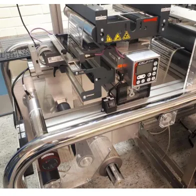
[image:2.612.207.403.376.572.2]Roll-to-roll (R2R) printing processes are high-volume, highly-parallel manufacturing methods used to produce electronics on flexible substrates [1]. Printable materials are deposited over large flexible substrates to form thin electrical structures (or webs) [2]. Compared to conventional electronics printing methods, R2R printing operates at low-processing temperatures and utilises low-cost substrates, such as polymers, papers or fabrics. This manufacturing technique is capable of patterning printed electronic circuits with a typical resolution of tens of micrometres at several metres per minute web speed. Feasible applications for R2R printed electronics include wearable technology, medical devices, wiring backplanes for system integration and low-profile sensors involved in the Internet of Things. An example of a R2R printer is shown in Fig. 1 where a web of wiring backplane is being printed. As the number of functional units in a R2R printing run is typically high, a fast in-process method to verify the printing quality can be critical, especially in applications where subsequent process steps, such as assembly of surface mounted devices or lamination, are needed. Thus, guaranteeing the outcome of R2R manufacturing by defect inspection avoids malfunctioning devices and improves product reliability.
Fig. 1. Roll-to-roll printed wiring backplane.
broadband sources or tunable lasers in the visible or infrared regions [6,7]. OCT and WSI offer relatively high-speed, high-resolution and non-contact 3D measurement of surface features, and OCT also allows detection deep within materials. It has been shown recently that OCT can be used for monitoring some structural properties of moving screen printed interdigitated electrodes in a simulated R2R process for speeds up to 1 m/min [8]. However, these techniques are very expensive and generate very large data sets that are difficult to be handled for in-process defect inspection.
A potential solution to increasing inspection speed is to conduct information processing by optical means. Early attempts at optical data processing date from the nineteenth century, and brief histories of the development of this field can be found in several review papers [9– 11] and books [12,13]. It is worth mentioning that among the forerunners of optical processing, Zernike developed the Nobel Prize-winning phase contrast microscopy [14]. Optical data processing is based on the combination of the principles of communications and optical systems, e.g. Fourier analysis, as a mathematical tool that has been widely used in the study of communication systems. Using the Fourier transforming properties of a lens, the input function to an optical system can be decomposed into a linear combination of elementary functions. Under the assumption of linearity, the representations of optical systems and the relation between the inputs and outputs can be simplified, such that the imaging process can be considered as a linear filtering operation and the optical system can be characterised by its transfer function [13]. The transfer function may be modified by placing a spatial filter at the Fourier plane of the optical system, such that the desired data processing, e.g. the linear mathematical operations including addition, subtraction, differentiation, convolution and correlation, can be carried out optically [10,11]. Typical applications of optical processing, realised by using spatial filters, are pattern recognition and signal detection [10,11]. These optical processing systems are usually realised using coherent illumination, but can also be achieved with incoherent illumination [12,15,16].
In this paper, we demonstrate a sensor, which is named the “all-optical difference engine” (AODE) here, to detect defects in printed electronics during R2R manufacturing processes. The working principle of the sensor is based on the theory of coherent optical subtraction and a self-comparison strategy. The development of a prototype AODE sensor using a digital camera is then discussed and demonstrated by inspecting defects in industrial printed electrical circuitry samples produced with two different R2R processes. The potential for using a photodiode as the detector and low-cost optical components for developing the sensor for high-speed pass-or-reject inspection is discussed.
2. Principle of AODE
2.1 Theory
The transmission functions of two objects can be compared optically through a technique called coherent optical subtraction. Assume two objects are positioned symmetrically about the optical axis in the front focal plane (x1, y1) of lens L1 (see Fig. 2) and are illuminated with a collimated laser beam. The separation between the two objects is 2d. The objects are defined by their transmittance functions as gA(x1 + d, y1) and gB(x1d, y1), respectively. The Fraunhofer diffraction pattern of the objects is found at the back focal plane (x2, y2) of L1, which gives the Fourier transforms of the objects’ transmittance functions. According to the shift theorem we obtain the field as
2 2 A 2 2 2 B 2 2 2
( , ) ( , ) exp 2 d ( , ) exp 2 d ,
U x y G x y j x G x y j x
f f
where GA,B(x2, y2) = FT{ gA,B(x1, y1)}, λ is the illumination wavelength and f is the focal length of L1. Note that the spatial frequencies kX and kY are related to the spatial coordinates (x2, y2) by the scaling factor λf, i.e. kX x2 f and kY y2 f .
To implement the optical subtraction of the two objects along the x-direction, a one-dimensional amplitude grating is used as the spatial filter, of which the transmittance function can be expressed as a cosine function for simplification of the mathematical derivation, as
2 2
2 2
1 ( ) 1 cos 2
1 1 1
1 exp 2 exp 2 ,
2
H x x
j x j j x j
(2)
where is the grating period and is the phase determined by the relative position of the grating on the x-axis. At the (x2, y2) plane, the Fourier transform of the object function is filtered only in the x-direction, such that the dependencies on y2 are ignored here. With the assumption of linearity, we obtain the field distribution in the x-direction as
2 2 A 2 2 B 2 2
A 2 2
B 2 2
A 2 2
B 2
( ) ( ) ( ) exp 2 ( ) exp 2
1 1
( ) exp 2 exp
2
1 1
( ) exp 2 exp
2
1 1
( ) exp 2 exp
2
1
( ) exp 2
2
d d
U x H x G x j x G x j x
f f
d
G x j x j
f d
G x j x j
f d
G x j x j
f d
G x j
f
1 x2 exp
j
. (3)
If f d and 2,then the exponential terms, exp(j), on the right-hand side of Eq. (3) reduce to ± j. It is interesting to note that optical addition can be achieved when 0 or π. Through lens L2, the field at the (x3, y3) plane is obtained as the Fourier transform of Eq. (3),
3 2 2
A 3 B 3 A 3 B 3
A 3 B 3
( ) FT ( ) ( )
( ) ( ) ( ) ( )
2
( 2 ) ( 2 ).
2 2
U x U x H x
j
g x d g x d g x g x
j j
g x d g x d
(4)
If a photon-sensitive device is placed at the (x3, y3) plane, the detected intensity is determined by the difference of the objects’ transmittance functions, and can be defined as
2 2
3 3 3 3 A 3 3 B 3 3
1
( , ) ( , ) ( , ) ( , ) .
4
I x y U x y g x y g x y (5)
Fig. 2. Illustration of coherent optical subtraction by spatial filtering. (a) Two identical optical transparencies and (b) the corresponding optical subtraction result; (c) defect present in one of the optical transparencies and (d) the corresponding optical subtraction result. The zeroth and ± 1 orders of diffraction are marked accordingly.
2.2 Inspection strategy
Defect detection by AODE requires a nominal object as the reference. This creates difficulties for in-process inspection, such as maintaining precise alignment between the reference and the test object while the test object may be moving at speeds of up to several metres per minute. However, the patterns produced in R2R processes, such as printed circuitries, are often continuous and/or repetitive, giving rise to the possibility of self-comparison using either a different part of the feature itself, or using a nearby repetitive feature, as the reference. Two options for self-comparison using test sample 3 as an example are illustrated in Fig. 3. The misalignment defect can be detected by comparing with the neighbouring circuit (option 1) or another portion of the same circuit printed a few seconds earlier or later (option 2). Self-comparison eliminates the need for an additional reference object and hence any addition or modification to the R2R hardware required for aligning the reference to the inspected product. Measurement accuracy is also improved by eliminating errors due to unsynchronised motion between the two objects.
Fig. 3. Illustration of self-comparison using nearby features as the reference. Red squares represent illuminated fields of view.
[image:5.612.188.421.488.589.2]reject products with a larger defect than is acceptable. A consumer-grade photodiode with kilohertz level sampling speed is more than capable of in-process inspection for R2R processes with a web speed of several metres per minute.
3. Experiment
3.1 Test samples
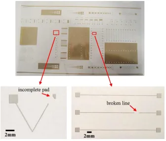
Test samples 1 and 2, as shown in Fig. 4, were R2R manufactured by the flexographic printing method. In this continuous process, the printed circuitry was formed as a relief on the surface of a soft printing plate and consequently transferred onto the substrate. The two samples involved were single conductors printed on a 125 μm thick Melinex ST506 PET film with water-based, heat-curable silver nanoparticle ink PFI-722 from Novacentrix. To demonstrate the capability of the developed inspection system, both samples included artificial manufacturing defects to mimic possible ink transfer failures on the printing plate. The defect on test sample 1 is an incomplete conducting pad, with material missing from a square of 2 mm nominal dimension. Test sample 2 includes a conducting line of 125 μm nominal width that is missing material for a length of approximately 2 mm.
Fig. 4. Test sample 1 (bottom left) with an incomplete pad and test sample 2 (bottom right) with a broken line due to ink transfer failure.
[image:6.612.139.475.288.574.2]misalignment of overlapping conductors. The misalignment width is approximately 0.75 mm. The illustrated defect is typical of multilayer layouts when the separate printing layers are not properly aligned. Such systematic manufacturing defects may lead to electrical failures, system non-functionality and poor product quality.
Fig. 5. Test sample 3 with a defect caused by misalignment between overlapping layers.
3.2 Experimental setup
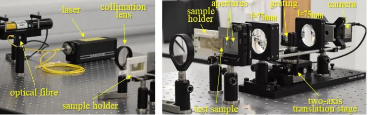
Based on the principle explained in section 2, a prototype AODE sensor was developed using off-the-shelf products. The setup of the developed prototype is shown in Fig. 6. The setup includes three parts: illumination, samples and AODE sensor. Illumination is provided by a helium-neon laser (nominal wavelength 633 nm) output with a single mode fibre (core diameter < 10 μm). The collimated beam reaches a diameter of 50 mm after the collimation lens (400 mm focal length). The expanded and collimated laser beam then illuminates the reference and the test object, both positioned by a sample holder. The sample holder was designed and additively manufactured to allow sliding motion of the objects in order to mimic in-process inspection during R2R processes, and to feature two rectangular hollow windows that determine the detection field of view (FOV) as the red squares shown in Fig. 3. The dimensions and positions of the two windows are adjustable in order to accommodate for a wide range of object dimensions and offset distances as described in Eq. (4). Light that passes through the apertures and the two objects is collected by the AODE sensor. The purpose of the two apertures is to limit illumination within the region of interest and avoid interference from higher order diffraction images of neighbouring features.
The AODE sensor consists of a 4f imaging system (75 mm focal length) and a Ronchi grating which is used as an amplitude grating (5 μm period) at the back focal plane of the Fourier transforming lens. The grating position can be adjusted with a two-axis translation stage to optimise the phase ( 2 as explained in the section 2.1) and the focus condition by transversal and axial translations, respectively. A CMOS camera (1280 × 1024 pixels) is used to receive the optical difference image (similar to the schema shown in Fig. 2). Specifications of the key optical components in the prototype are listed in Table 1.
[image:7.612.122.493.556.672.2]Table 1. Specifications of the optical components in the prototype AODE.
Laser wavelength 633 nm Imaging lens focal length 75 mm Grating type Amplitude Grating period 5 μm Image sensor pixel size 1280 × 1024 Image sensor type CMOS
4. Results and discussion
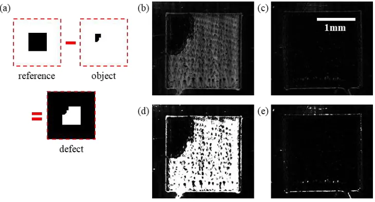
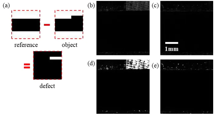
The captured defect (incomplete pad) in test sample 1 is shown Fig. 7. The reference and object images are illustrated in Fig. 7(a), along with the expected difference image. Black areas in the reference and object images indicate the presence of optical obstacles (i.e. ink), while white areas indicate optical transparency (i.e. clear substrate). Any defect will appear bright in the resulting difference image. The difference image captured by the CMOS camera, as shown in Fig. 7(b), shows the detected defect. The pores observed in the difference image indicate the presence of dust particles on the transparent substrate. For comparison, Fig. 7(c) shows another difference image captured when inspecting a high-quality feature without discernible defects. A simple threshold can be set at, e.g. 15% of the detector’s saturation value, in order to saturate the pixels that receive an intensity higher than the threshold, thus separating defects from the background as shown in Fig. 7(d) and Fig. 7(e). After applying the threshold, the saturated areas with respect to the FOV correlate to the dimension of the defect. The saturated areas in Fig. 7(d) and Fig. 7(e) are 39.8% and 0.7%, respectively. The thresholding can be easily applied to the system which uses a photodiode as the detector, and the processing time of the thresholding should be negligible. If the quality of the print is within tolerance, the defects found in Fig. 7(e) can be considered as detection noise. The ability of the AODE sensor to detect defects can be characterised by the defect-to-noise ratio defined as the ratio between the saturated areas in Fig. 7(d) and Fig. 7(e), which is 56.6 for this specific defect. Note that the ratio should be much larger than unity in order to make a valid inspection decision.
Fig. 7. Optical subtraction of test sample 1: (a) illustration of the reference image, the object image and the defect, (b) the difference image showing materials missing from the conducting pad, (c) the difference image when no defect is present, (d) binarised difference image showing the defect, and (e) binarised difference image when no defect is present.
[image:8.612.125.490.419.616.2]likely a characteristic of the ink transfer process. The saturated areas with respect to the FOV in Fig. 8(d) and Fig. 8(e) are 5.1% and 0.1%, respectively, resulting in a defect-to-noise ratio of 74.8. Features down to 10 μm in size can be clearly resolved.
Fig. 8. Optical subtraction of test sample 2: (a) illustration of the reference image, the object image and the defect, (b) the difference image showing materials missing from the conducting line, (c) the difference image when no defect is present, (d) binarised difference image showing the defect, and (e) binarised difference image when no defect is present.
The captured misalignment defect in test sample 3 is shown in Fig. 9. The defect, which registers as a sharp increase or decrease in the width of the conducting line, appears in the form of a rectangular bar. It is also observed that dust particles on the sample substrate have contributed to noise in the difference image, resulting in bright speckles outside the defect area and dark spots inside the defect area. The saturated areas with respect to the FOV in Fig. 9(d) and Fig. 9(e) are 5.4% and 0.2%, respectively, resulting in a defect-to-noise ratio of 25.5.
Fig. 9. Optical subtraction of test sample 3: (a) illustration of the reference image, the object image and the defect, (b) the difference image showing misalignment of two patterns, (c) the difference image when no defect is present, (d) binarised difference image showing the defect, and (e) binarised difference image when no defect is present.
[image:9.612.122.494.132.263.2] [image:9.612.129.483.396.586.2]detection as long as the objects remain in the FOV. Both the rotational and translational movements of the objects during the manufacturing process are well within tolerable limits. The third type of misalignment is caused by the mismatch of the physical separation between the two features under comparison and the parameters of the AODE sensor, including wavelength, focal length of the Fourier transforming lens and the grating period, i.e. d f . The separation can be matched again by adjusting the grating period using, e.g. a chirped grating, or by adjusting the illumination wavelength using a tunable laser.
We have also used polydimethylsiloxane (PDMS) gratings replicated from master silicon gratings [17] to achieve the optical subtraction effect; although this grating cannot be considered as an amplitude grating that is assumed in the theoretical derivation. With such a grating, the image sharpness is not as good as with a thin amplitude grating, likely due to the large thickness of the PDMS and the glass substrate. However, this type of grating has the advantage of being cost-effective.
In this study, a digital camera was used to record the difference image in order to evaluate and illustrate the performance of the AODE sensor. As discussed in section 2.2, decisions on process control are often reduced to a simple criterion of whether the size of the defect is acceptable. In such cases, a photodiode can be used to replace the camera as the detector and achieve determination of defect dimension at higher speed and lower cost. The voltage of the photodiode is expected to be proportional to defect size. Several objects with defects of various dimensions have been inspected using both the camera and a photodiode as the detector. The voltage of the photodiode (Texas Instrument, OPT101), sampled by a 10-bit analogue-to-digital converter onboard an Arduino Uno microcontroller, was found to correlate very well with the sum of the pixel intensity of the camera images. The high sampling speed of the photodiode is critical to reducing motion blur when determining defect dimensions, thus enabling in-process pass-or-reject inspection. The cost of a photodiode is also significantly lower than a CMOS sensor, which is highly desirable, especially when building parallel systems for inspection of larger areas. The cost of the light source in the parallel inspection systems can also be reduced by using a fibre optic coupler with multiple output ports to illuminate multiple areas.
5. Conclusion
This work has demonstrated an all-optical difference engine sensor for detecting defects in printed electronics during roll-to-roll manufacturing processes. The sensor is based on the principle of coherent optical subtraction, which can be performed at high speed because the data post-processing at the software level is virtually eliminated. A prototype was developed with off-the-shelf components and a digital camera. The capability of the developed sensor was demonstrated by inspecting defects on industrial printed electrical circuitry samples and it was found to be able to detect defects down to micrometre level over a field of several millimetres. The self-comparison strategy also eliminates the need for a physical reference object to be added in the inspection system and improves the flexibility of the system. Lastly, the use of low-cost gratings, fibre optic illumination and photodiodes and microcontrollers for detection makes it technically and economically more feasible to build parallel inspection systems for the in-process pass-or-reject inspection of industrial R2R processes.
Funding
Acknowledgments