Rochester Institute of Technology
RIT Scholar Works
Theses Thesis/Dissertation Collections
1-16-2014
Reduction of Line Edge Roughness (LER) in
Interference-Like Large Field Lithography
Burak BaylavFollow this and additional works at:http://scholarworks.rit.edu/theses
This Dissertation is brought to you for free and open access by the Thesis/Dissertation Collections at RIT Scholar Works. It has been accepted for inclusion in Theses by an authorized administrator of RIT Scholar Works. For more information, please [email protected]. Recommended Citation
REDUCTION OF LINE EDGE ROUGHNESS (LER) IN
INTERFERENCE-LIKE LARGE FIELD LITHOGRAPHY
by
Burak Baylav
A dissertation submitted in partial fulfillment of the requirements for the
degree of Doctorate of Philosophy in Microsystems Engineering
Microsystems Engineering Program
Kate Gleason College of Engineering
Rochester Institute of Technology
Rochester, New York
REDUCTION OF LINE EDGE ROUGHNESS (LER) IN
INTERFERENCE-LIKE LARGE FIELD LITHOGRAPHY
by
Burak Baylav
Committee Approval:
We, the undersigned committee members, certify that we have advised and/or supervised the candidate on the work described in this dissertation. We further certify that we have reviewed the dissertation manuscript and approve it in partial fulfillment of the requirements of the degree of Doctor of Philosophy in Microsystems Engineering.
Dr. Bruce W. Smith Date
Committee Chair and Dissertation Advisor
Dr. Robert Pearson Date
Committee Member
Dr. Zhaolin Lu Date
Committee Member
Dr. Mark Schattenburg Date
Committee Member
Dr. Pawitter Mangat Date
Committee Member
Certified by:
Dr. Bruce W. Smith Date
Director, Microsystems Engineering Program
Dr. Harvey J. Palmer Date
ABSTRACT
Kate Gleason College of Engineering Rochester Institute of Technology
Degree: Doctor of Philosophy Program: Microsystems Engineering
Author’s Name: Burak Baylav
Advisor’s Name: Dr. Bruce W. Smith
Dissertation Title: REDUCTION OF LINE EDGE ROUGHNESS (LER) IN INTERFERENCE-LIKE
LARGE FIELD LITHOGRAPHY
Line edge roughness (LER) is seen as one of the most crucial challenges to be addressed in advanced technology nodes. In order to alleviate it, several options were explored in this work for the interference-like lithography imaging conditions.
The most straight forward option was to scale interference lithography (IL) for large field integrated circuit (IC) applications. IL not only serves as a simple method to create high resolution period patterns, but, it also provides the highest theoretical contrast achievable compared to other optical lithography systems. Higher contrast yields a smaller transition region between the low and high intensity parts of the image, therefore, inherently lowers LER. Two of the challenges that would prohibit scaling IL for large field IC applications were addressed in this work: (1) field size limitations, and (2) magnification correction (i.e., pitch fine-tuning) ability.
Experimental results showed less than 0.5 nm pitch adjustment capability using fused silica wedges mounted on rotational stages at 300 nm pitch pattern. A detailed discussion on maximum practical IL field size was outlined by considering the subsequent trim exposures and optical path difference effects between the interfering diffraction orders. The practical limit on the IL field size was assessed to be 10 mm for the conditions specified in this work.
ACKNOWLEDGMENTS
Here, I would like to acknowledge the people who helped me to grow not only as
an aspiring researcher in a challenging field, but also inspired me to be a better person in
a challenging world in the recent years of my life.
Earning the doctorate degree was not an easy task, at times it felt draining both
physically and emotionally. The following people will forever have my gratitude for
being my support, my teacher, my rock, my advisor, my friend, my colleague and more
importantly my believer even when I started to doubt myself.
I would like to thank Dr. Bruce Smith for introducing me to the field of
nanolithography. Since the day I met him, he inspired me to be an innovative researcher.
He has given me many opportunities that led me to where I am today. I am also thankful
to my past and present group members Chris Maloney, Zac Levinson, Andrew Estroff,
Germain Fenger, Andrew Burbine, Monica Sears, Peng Xie, Neal Lafferty, Anatoly
Bourov, Jianming Zhao, and Steve Smith. Anytime I felt stuck or felt frustrated, our
brainstorming and heated discussions always helped me solve the challenges I faced. I
also want to thank our department secretary Lisa Zimmerman for tirelessly answering the
most tedious questions I had, always with a warm smile on her face. I will miss them
dearly.
I would also like to thank my committee members Dr. Pawitter Mangat, Dr. Mark
Schattenburg, Dr. Robert Pearson, and Dr. Zhaolin Lu for their invaluable guidance and
I don’t think I would be able to finish this work without the support I got from
Matt Burgess, my mom Nisa Serefli, my brothers Murat Baylav and Mert Baylav. They
believed in me and encouraged me whenever I felt depressed and exhausted which
happened more than one occasion, especially towards the end. I know the sacrifices they
have made for me; I can only hope they know how much I appreciate them.
I would like to thank IMEC research facility in Leuven, Belgium, for their help
with important parts of the experiments. I would like to especially acknowledge Joost
Bekaert and Alessandro Vaglio Pret, both of whom are extremely knowledgeable and
great people that I admire.
Finally, this work was made possible with the financial aid from Semiconductor
Research Corporation (SRC), Global Research Corporation (GRC) and
GLOBALFOUNDRIES through the task number 2126.002. I also acknowledge EUV
Technology’s SuMMIT and KLA Tencor’s PROLITHTM
for the free use of their
Table of Contents
Abstract ... i
Acknowledgments... ii
List of Figures ... vi
List of Tables ... xiii
List of Acronyms ... xiv
1. Introduction to Lithography ... 1
1.1 Background of Lithography ... 2
1.2 Excimer Laser Review ... 4
1.3 Next Generation Lithography (NGL) Approaches... 6
1.3.1 Double patterning (DP) technology ... 7
1.3.2 EUV lithography technology ... 8
1.3.3 Maskless lithography technology ... 9
1.3.4 Nanoimprint lithography technology ... 10
1.3.5 Directed self-assembly technology ... 12
1.3.6 Interference lithography ... 14
1.4 One Dimensional Regular Design Approaches ... 17
1.5 Problem Statement ... 18
2. Theory and Background ... 21
2.1 Coherent Image Formation... 21
2.1.1 Effect of partial coherence on imaging ... 24
2.1.2 Effect of aberrations on imaging... 26
2.1.3 Effect of vibration on imaging ... 27
2.2 Reduction Talbot Specific Derivations ... 31
2.2.1 Effect of OPD on field size ... 35
2.3 Line Edge Roughness (LER)... 37
2.3.1 Mask roughness transfer ... 47
2.3.2 Previous LER mitigation attempts ... 51
2.4 Speckle Theory in Imaging ... 53
2.5 Pupil Filtering Applications ... 56
2.7 Translational Image Averaging: Characterization and Measurement ... 60
3. Approach and Experimental Procedure ... 65
3.1 IL Specific LER Mitigation Studies ... 65
3.1.1 Translational image averaging for LER smoothing ... 65
3.1.2 Pupil plane filtering... 71
3.2 Magnification Correction Studies for Machine Mix and Match ... 85
3.2.1 Approach ... 86
3.2.2 Experimental procedure ... 88
3.3 Effect of OPD on Field Size ... 89
3.3.1 Approach ... 91
3.3.2 Experimental procedure ... 93
4. Results and Discussions ... 95
4.1 IL Specific LER Mitigation Studies ... 95
4.1.1 Aerial image averaging via directional translation ... 95
4.1.2 Pupil plane filtering... 102
4.2 Magnification Correction Results ... 114
4.3 Maskless IL Results ... 115
5. CONCLUSIONS... 117
6. Appendix A ... 119
7. Appendix B ... 123
8. Appendix C ... 130
LIST OF FIGURES
Figure 1.1: A simplified schematic of a projection lens system. ...2
Figure 1.2: Lithography exposure tool potential solutions for MPU and DRAM ...7
Figure 1.3: Process flows for DE, DP, and SP approaches ...8
Figure 1.4: Comparison of DUV and EUV aerial images for 45 nm line end structures ...9
Figure 1.5: Comparison of electron beam lithography techniques for single and multiple
beam approaches ...10
Figure 1.6: (a) Schematic of simple NIL process showing mold imprinting and RIE. The
SEM images of the (b) mold and (c) resulting PMMA profiles before RIE ...11
Figure 1.7: Defect classification results for the process of record by [64]. Out of 91
randomly selected defects for SEM review, zero was classified as a fundamental
DSA polymer phase separation defect ...13
Figure 1.8: Different IL setups utilized in literature (reproduced from [85]). ...15
Figure 1.9: 6T SRAM. Left: GRD. Right: 2D design with 3 problematic locations ...17
Figure 1.10: SEM images showing experimental hybrid optical maskless approach results
in which IL and trim exposures were performed in the same resist ...18
Figure 2.1: Monochromatic plane waves intersecting at the origin with half angle of θ. .22
Figure 2.2: (a) Definition of partial coherence. (b) Effect of partial coherence on imaging
for an isolated 500 nm wide line. ...25
Figure 2.3: (a) Measured time vibration data for an optical stepper. (b) Corresponding
histograms based on 5-s and 60-s intervals. (c) Triangular vibration histogram
approximation to (b) ...28
Figure 2.4: (a) Sinusoidal vibration of a single frequency. (b) Its histogram ...29
Figure 2.6: Effect of optical path difference (OPD) on interference of correlated wave
groups (modified from[108]). ...35
Figure 2.7: Effect of OPD and source bandwidth (i.e. beating) on image contrast
degradation across the field for 193 nm ArF laser. Three different source
bandwidths are considered: broadband, 100 pm FWHM, and 2 pm FWHM. ...36
Figure 2.8: LER framework proposed by [110]...39
Figure 2.9: ITRS LWR roadmap, shown with total LWR (3σ) and contribution of speckle
for 5 different resists. Resist A is highlighted for discussion ...40
Figure 2.10: SEM images depicting LER for varying resist thicknesses and for two resists
with different sensitivities. Resist B has 2.5X more photo-acid generator
concentration than resist A ...41
Figure 2.11: LER degradation as a function of contrast loss shown for (a) UV6
chemically amplified resist, and (b) PMMA chain scissioning resist ...42
Figure 2.12: LER comparison of 90 nm dense line/space pattern for an IL system
(Amphibian) and ASML /1150i . ...43
Figure 2.13: The effect of LWR on (a) Vth, (b) Ioff variability ...44
Figure 2.14: The FinFET device performance variability as a function of roughness
frequency for the same amplitude ...45
Figure 2.15: (a) The mask roughness influence region [129]. (b) Mask roughness
contribution as a function of resist quality and optical system cut off frequency .46
Figure 2.16: (a) Ideal mask diffraction information at the pupil plane. (b) Roughness
Figure 2.17: Schematic of two main sources of mask induced roughness for EUV:
absorber roughness and replicated surface roughness ...50
Figure 2.18: Effect of (a) special rinse, and (b) ion beam smoothing techniques on LER
PSD … ...52
Figure 2.19: Effect of increasing pulse duration with respect to the coherence time.
Integrated dose (W) has less of a variation for longer pulses. T<<τc corresponds to
the conventional (static) pattern ...53
Figure 2.20: Pupil filtering idea. Left: No filter case, right: with filter case ...56
Figure 2.21: Enhancing resolution of EUV ADT tool by using a pupil plane amplitude
filter at 22 nm half image pitch for resist A ...57
Figure 2.22: Micrographs of stitched areas by optical and scanning electron microscope 58
Figure 2.23: (a) Parallel SBIL, (b) Doppler SBIL . ...59
Figure 2.24: Schematic of achromatic IL set up for 100 nm period image pattern ...60
Figure 2.25: Examples of vendor specifications of a typical toolset used in 250 nm to 700
nm fabrication and VC curves from A to E ...62
Figure 2.26: Comparison of pre- and post- startup vertical vibration for (a) narrow band
data, (b) one third octave data ...64
Figure 3.1: Contrast loss due to transverse shift error for uniform and sinusoidal type
motions. ...66
Figure 3.2: (a) Mask with anti-correlated (L1), random (L2), and perfectly correlated (L3)
rough lines. (b) Aerial image from single pass exposure. (c) Aerial image from
Figure 3.3: (a) Interference lithography set up for the aerial image averaging experiments
[18]. (b) Translation approach: the wedge is moved in x direction at mid
exposure, resulting in shift of the image in y direction (along the lines). (c)
Co-processed nominal and translated dies on the same wafer piece to minimize
processing related variations. ...68
Figure 3.4: Exposed module on the scanner and imaging conditions for each die . ...71
Figure 3.5: (a) 1D mask with smooth vertical line space features and corresponding
diffraction information. (b) Mask with absorber roughness and corresponding
diffraction information. Dashed regions: main diffraction orders coming from
smooth vertical features ...72
Figure 3.6: Collection of (a) many diffraction orders or (b) just the main diffraction
orders at the pupil plane. Top down views of photoresist profiles generated with a
constant threshold resist model are shown for each case ...73
Figure 3.7: ASML’s FexWave wavefront manipulator ...74
Figure 3.8: (a) Programmed defect mask and the measurement locations along two
cutlines. (b) Diffraction pattern of the mask with optimized dipole. (c) Effect of
different aberrations on the aerial image profile and ΔCD along two cut locations.75
Figure 3.9: (a) Definition of an ideal (smooth) mask with vertical line space pattern, and
corresponding (b) anti-correlated and (c) correlated programmed roughness masks
………...76
Figure 3.10: (a) Roughness transfer as a function of introduced defocus. (b) Optimized
Figure 3.11: (a) White noise mask. (b) Diffraction information at the pupil plane with
optimized dipole illumination. Resulting aerial images for the (c) nominal case,
(d) phase filtered case. ...78
Figure 3.12: (a) Top-down aerial image intensity distribution for nominal anti-correlated
and correlated masks. (b) Corresponding phase filtered distribution. (c)
Comparison of intensity distributions along the cutlines. ...79
Figure 3.13: (a) Aerial image Bossung curves for nominal and phase filtered cases at two
cutlines, (b) ΔCD between the two cutlines for nominal and phase filtered cases.
“Nominal” refers to without the filter case. ...80
Figure 3.14: Diffraction information for 200 nm and 500 nm roughness periods. ...81
Figure 3.15: Optimization of phase filters for 200 nm (W1) and 500 nm (W2) roughness
periods and corresponding Zernike combinations to create them. ...82
Figure 3.16: (a) MATLAB surface fitting routine. (b) Effect of cost function inclusion on
the fit efficiency. ...83
Figure 3.17: (a) Target and experimental filters (ΔΦAB ≈ 0.25 waves). (b) Zernike
coefficients for the target and experimental filters. ...85
Figure 3.18: Effect of pitch error in overlay of subsequent exposures. ...86
Figure 3.19: (a) Talbot set up with wedges for pitch fine tuning. (b) The definition of
deviation angle from the wedge prism. (c) Deviation angle as a function of
incident angle for the wedge prism with apex angle of 1.05°. ...87
Figure 3.20: (a) Dies exposed over various θ, (b) Line-outs measured over 10 line/space
pairs across the SEM field to calculate the pitch. ...89
Figure 3.22: Maskless IL set up for studying OPD effect on contrast loss. ...93
Figure 4.1: Initial problems associated with the interference lithography experiments: (a)
ringing issue and (b) pattern collapse issue. (c) Spatial filtering. ...95
Figure 4.2: (a) Co-processing of static (nominal) and image averaged (translated) dies.
Comparison of nominal case LER to image averaged case LER with translation
amounts of (a) 250 nm, (b) 500 nm, and (c) 750 nm. ...96
Figure 4.3: Effect of contrast loss through flood exposure on LER PSD (a) for 139 nm
thick resist, (b) for 75 nm thick resist ...97
Figure 4.4: (a) Location dependency is observed for IL experiments. (b) Imperfect mask
is one of the sources of variations. (c) Intra-field LER values ...99
Figure 4.5: SEM pictures of 3 µm long patterns for the pitches of (a) 130 nm (Die 1),
(b) 140 nm (Die 1), (c) 150 nm (Die 1), (d) 150 nm (Die 2), and (e) 150 nm
(Die 8). ...100
Figure 4.6: Effect of aerial image averaging on LER PSD for die 3 and die 8. Best case
mitigation was for die 8 and highlighted with dashed box ...102
Figure 4.7: Comparison of roughness transfer for nominal and filtered cases through
focus for 200 nm and 500 nm roughness periods. ...103
Figure 4.8: Nominal and phase filtered SEM images for 200 nm roughness period in (a)
anti-correlated and (b) correlated fashions. ...104
Figure 4.9: Nominal and phase filtered SEM images for 500 nm roughness period in (a)
Figure 4.10: Through slit LWR values for the nominal and wavefront cases programmed
with periods of (a) 200 nm and (b) 500 nm, in both correlation types. Error bars
correspond to average 1σ LWR variations. ...106
Figure 4.11: Through slit LER values for the nominal and phase filtered cases
programmed with periods of (a) 200 nm and (b) 500 nm, in both correlation types.
Error bars correspond to average 1σ LER variations. ...107
Figure 4.12: Through slit LF LER values for the nominal and wavefront cases
programmed with periods of (a) 200 nm and (b) 500 nm, in both correlation types.
Error bars correspond to average 1σ LER variations. ...108
Figure 4.13: Slit center LER values for (a) 200 nm, and (b) 500 nm roughness periods at
the slit center. Both correlation types are considered ...109
Figure 4.14: LER PSD of nominal and phase filtered wafers. Comparison for 200 nm
roughness period with amplitudes of (a) 1nm/edge and (b) 5nm/edge. Comparison
for 500 nm roughness period with amplitudes of (c) 1 nm/edge and (d) 5 nm/edge.110
Figure 4.15: Experimentally calculated correlation factor for (a) 200 nm, (b) 500 nm
roughness periods...112
Figure 4.16: Effect of filtering on (a) smooth line 3σ LWR through bias. (b) NILS
reduction and LWR increase through roughness amplitude for the filtered case.113
Figure 4.17: Pitch fine tuning via change in rotational angle of the wedge prism holder.
Dashed line corresponds to a trend line fit to the experimental data points. ...115
LIST OF TABLES
Table 1.1: Comparison of Excimer and Solid State Lasers (modified from [92]). ...16
Table 2.1: Summary of vibration tolerance at k1=0.64 and σ=0.8 ...30
Table 2.2: 2011 Edition ITRS LWR requirements (generated from data of [32]) ...37
Table 2.3: Acceleration measurement methods and properties ...61
Table 2.4: Application and interpretation of the generic VCC as shown in Fig. 2.25. ...63
LIST OF ACRONYMS
ACP Air cushion press
ADT Alpha demo tool
BARC Bottom anti-reflective coating
CD Critical dimension, [nm]
CF Correlation factor
CoO Cost of ownership
DE Double exposure
DIW Deionized water
DOF Depth of focus
DP Double patterning
DSA Directed self-assembly
DUV Deep ultraviolet region of the radiation (100–300 nm wavelength)
EBL E-beam lithography
EL Exposure latitude
EUV Extreme ultraviolet region of the radiation (10–30 nm wavelength)
EUVL Extreme ultraviolet lithography
FEM Focus-exposure matrix
FIB Focused-ion-beam
FWHM Full width half maximum
GRD Gridded regular design
HIF High index fluid
HVM High volume manufacturing
IC Integrated circuit
IL Interference lithography
ITRS International Technology Roadmap for Semiconductors
LELE Litho-etch-litho-etch
LER Line edge roughness
LFLE Litho-freeze-litho-etch
LPLE Litho-process-litho-etch
LTF Line edge roughness transfer function
LWR Line width roughness
MAPPER Multi aperture pixel by pixel enhancement of resolution
MEEF Mask error enhancement factor
ML2 Maskless lithography
MTF Modulation transfer function
NA Numerical aperture
NGL Next generation lithography
NIL Nanoimprint lithography
NILS Normalized image log slope
OPC Optical proximity correction
OPD Optical path difference
OPL Optical path length
OTF Optical transfer function
PAG Photo-acid generator
PML2 Projection maskless lithography
POR Process of record
PS Pitch splitting
PSM Phase shifting mask
REBL Reflection electron beam lithography
RMS Root-mean-square
RSR Replicated surface roughness
SBIL Scanning beam interference lithography
SEM Scanning electron microscope
SFIL Step-and-flash imprint lithography
SMO Source mask optimization
SP Spacer patterning
SR Surfactinated rinse
UV Ultraviolet region of the radiation (150–400 nm wavelength)
VCC Vibration criteria curves
1.
I
NTRODUCTION TO
L
ITHOGRAPHY
Since the invention of the transistor more than 60 years ago, semiconductor
industry has witnessed significant progress in device manufacturing. The developments
resulted in more powerful and sophisticated products that are also cost effective. Some of
these recent developments can be listed as realization of strained silicon, low-k insulators
and high-k gate metal. More recently, Intel announced their 22 nm technology node
which uses a tri-gate transistor to boost the gate control over the short channel, instead of
the conventional planar transistors [1, 2].
In integrated circuit (IC) manufacturing process, the photolithography step is
repeated several times; hence, it accounts for about 30% of the cost of manufacturing [3].
In addition, it is also the photolithography step that limits the critical dimension of the
printed features; hence, the speed of transistors. The reduction in device scales has
resulted in the trend of doubling of number of transistors on a chip approximately every
two years, which is widely known as Moore’s law [2]-[4].
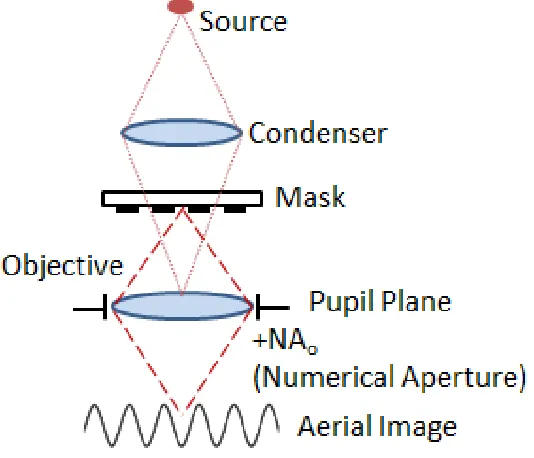
Figure 1.1 shows a simple projection lithography system set up composed of a
deep-UV (DUV) source, a condenser lens, mask, and an objective lens located at the
pupil plane with a size defined by the numerical aperture (NA) of the system. The
projection system creates an aerial image that is approximate to the patterns defined in
the mask, but at a fixed reduction ratio (usually reduction factor of 4). The aerial image
subsequently exposes a photo-reactive medium called “photoresist.” Depending on the
either positive tone or negative tone imaging, where the former requires removal of the
[image:21.612.190.457.145.374.2]photoresist materials that corresponds to the transparent parts on the mask [3, 5].
Figure 1.1: A simplified schematic of a projection lens system.
1.1 Background of Lithography
The main goal of semiconductor manufacturing has been to produce smaller,
faster and more sophisticated devices, which is achievable by reducing the feature sizes
through lithography processes. For periodic features, the minimum resolution of an
imaging system is characterized by the “Rayleigh’s criterion”, which is given as
(1.1)
where critical dimension, exposure wavelength, refractive index of imaging medium, half
angle subtended by the objective lens, and numerical aperture of the system are denoted
which can be pushed close to its theoretical limit of 0.25 by utilizing resolution
enhancement techniques (RET) [7, 8]. Some of the resolution enhancement techniques
that have been pursued for further improvements can be listed as optical proximity
correction (OPC) [9, 10], phase shifting mask (PSM) [11], off axis illumination [12, 13],
and source mask optimization (SMO) [14, 15].
Another criterion that is important in characterizing the performance of the
lithography system is called the “Depth of Focus” (DOF), given as [3]
(1.2)
where k2 is another process dependent factor. Rayleigh’s criterion shows that in order to
reduce the critical dimension, one can shift from longer wavelength to shorter
wavelengths, increase the numerical aperture of the objective lens or improve the
lithographic process. Over the past decades, the illumination wavelength has been
reduced from mercury lines (436 nm g-line and 365 nm i-line) down to deep-ultraviolet
(DUV) wavelengths of KrF (248 nm), ArF (193 nm), and F2 (157 nm). The wavelength
reduction trend is concluded at immersion 1.35 NA ArF. As a next step, major tool
providers are investing extensively on infrastructures of 13.5 nm wavelength extreme UV
(EUV) lithography [16].
Immersion ArF lithography (sometimes combined with pitch splitting approach)
is the workhorse of current production lines. Currently, down to 40 nm features can be
resolved with state-of-the-art water immersion projection lithography employing 193 nm
ArF excimer laser source with 1.35 NA catadioptric projection optics [17]. When
Aside from reducing the minimum device dimensions, the tolerances on the
fidelity of the lithography defined patterns are becoming much more stringent. The
impact of sidewall roughness on photoresist lines, usually referred to as the line edge (or
width) roughness has been shown to impact the electrical performance of the
semiconductor devices significantly. If it is not addressed, it might limit the useful
resolution [3]. The ideas presented in this work, such as aerial image averaging via
directional translation [18] and pupil plane filtering [19], might help reduce the roughness
seen in interference-like lithography conditions.
1.2 Excimer Laser Review
The source is one of the most crucial parts of illumination systems in optical
lithography. It determines the coherency of imaging, quality of patterns, and throughput
of the whole system. Therefore, it is important to understand important properties of the
illuminating source.
Excimer laser lithography systems are superior to e-beam writers in terms of
throughput. Since 1988, through the trials for 64 Mbit DRAM, excimer lasers have
become the main choice in commercial high volume manufacturing (HVM) [20].
There are certain differences between a mercury lamp and excimer lasers, which
are related to the characteristics of the short wavelength excimer lasers and high power
pulse energy with short pulse durations (i.e., pulsed lasing). Sometimes, such large power
differences between the excimer laser and mercury sources can be listed as the small
divergence values and pulse to pulse energy fluctuations [20].
The natural linewidth (full width half maximum-FWHM) of excimer lasers is
usually between 0.3 nm and 1 nm. Such bandwidth values at nm levels are too large for
chromatic aberrations in a lens system and needs to be reduced below 3 pm by utilizing
line narrowing modules, such as etalons, dispersive prisms, gratings or their combinations
in the cavity of the laser [20, 21].
Line narrowing through two etalons with different gap thicknesses in the cavity of
the laser provides high efficiency and sufficiently narrow bandwidths. Using prisms,
instead, provides high thermal stability and high damage threshold, at the cost of low
dispersion efficiency. Therefore, it is quite common to use combination of prisms and
gratings as dispersive elements in current lasers. Using such techniques, spectral
bandwidth of the laser can be as low as 1.0 to 1.5 pm [21-28].
Wavelength stability is crucial for the performance of imaging since even a 1 pm
drift in central wavelength might lead to more than 0.1 μm shift in focal plane for a
typical chromatic lens [29]. Therefore, wavelength is monitored continuously by
techniques such as observing the fringe formation by a monitoring etalon [22, 23, 25, 28],
or measuring the wavelength difference of the absorption line of a gas cell [20, 26].
Narrowing the linewidth increases the temporal coherence of the beam. It also
increases the spatial coherence due to the reduced divergence angle. However, increased
coherence might result in unwanted interference effects and speckle patterns, which are
The excimer lasers are pulsed and the output energy of varies from pulse to pulse
[20, 31]. This fluctuation is problematic when a fixed number of pulses were
accumulated to reach the required dose at the wafer plane. In order to guarantee a certain
amount of dose accuracy (A), one can define the minimum number of pulses to be
accumulated (N) as follows [20]
[ ] (1.3)
where ∆P/P defines the pulse to pulse energy stability. For a scenario requiring 0.5% dose
accuracy and 5% fluctuation from pulse to pulse, more than 100 pulses are required [20].
1.3 Next Generation Lithography (NGL) Approaches
Fig. 1.2 shows the 2011 edition of ITRS [32], summarizing applicable
technologies for next technology nodes starting from 2011 up to 2026. For the 32 nm
node, ArF lithography is sufficient enough by utilizing pitch splitting techniques.
However, for more advanced nodes, the process complexity and the demands increase.
For instance, Intel recently revealed its 22 nm node 3D transistors to enable
improved control of the channel below the gate region. The gate surrounds the silicon
channel in three directions, which provides significant energy efficiency [1]. For sub-22
nm DRAM technologies, introduction of non-optical lithography approaches is seen as a
Figure 1.2: Lithography exposure tool potential solutions for MPU and DRAM [32].
1.3.1 Double patterning (DP) technology
In order to push k1 beyond its theoretical limit of 0.25 and achieve smaller
devices, two basic processes known as “Pitch Splitting (PS)” and “Spacer Patterning
(SP)” can be utilized [33-36]. PS is achievable via Litho-Etch-Litho-Etch (LELE) or
Freeze-Etch (LFLE) processes [37]. The latter is also known as
Litho-Process-Litho-Etch (LPLE). The spacer patterning approach multiplies the pitch by
sidewall spacer formation to the sides of the mandrel layer [34, 38]. Though, it has one
critical lithography step, it requires a critical deposition and etch step very similar to
spacer-like processes. Subsequent cut (trim) mask lithography is needed to remove excess
parts of the layer. In a Litho-Etch-Litho-Etch method a sacrificial hard mask is used to
this method is proportional to the complexity of processing it [39]. Fig. 1.3 shows the
basic process flows for the pitch splitting and spacer multi-patterning approaches [32-34,
[image:27.612.113.538.163.397.2]36, 38].
Figure 1.3: Process flows for DE, DP, and SP approaches [32].
1.3.2 EUV lithography technology
Improvement of low k1 values is troublesome and hard to achieve. From
Rayleigh’s criteria, the next logical option to improve minimum resolution is the
wavelength reduction. Therefore, EUV is currently viewed as a strong candidate as far as
the NGL options are concerned [40]. However, there exist many problems in terms of
masks, material properties, and available source power [41-43].
The wavelength of EUV is fourteen times smaller than the deep-UV (DUV)
wavelengths. By utilizing 0.25 NA EUV and a modest k1 value of 0.6, a 32 nm half pitch
Fig. 1.4 shows the benefit of using EUV instead of DUV in terms of image
fidelity, by comparing 45 nm line-end structure aerial images. With a 1.30 NA ArF
immersion tool, the image is not well defined. However, due to EUV’s inherent capacity
to print smaller features, image fidelity is high even with a small NA value of 0.25 [40].
The main obstacle for EUV to be ever used in HVM is the dim source power resulting in
less than the desired throughput levels in a HVM environment.
Figure 1.4: Comparison of DUV and EUV aerial images for 45 nm line end structures
[40].
1.3.3 Maskless lithography technology
Maskless lithography (ML2) is another option proposed for sub 22 nm nodes and
most of the time refers to patterning photoresists without optical illumination, such as
zone-plate-array lithography [44], and focused-ion-beam (FIB) lithography [45, 46].
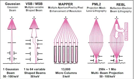
E-beam lithography [47, 48] is the most common maskless method, where a
focused electron beam is scanned on a photoresist material to create high resolution
patterns with good accuracy. Single beam writing systems have extremely slow writing
times; therefore, multiple-beam writing approaches have been implemented to overcome
Some of such maskless lithography systems where multitude of beams are
coordinated with respect to their size, dose and placement can be listed as Multiple
Aperture Pixel by Pixel Enhancement of Resolution (MAPPER) [50, 51], Projection
Maskless Lithography (PML2) [52], and Reflective Electron Beam Lithography (REBL)
[53] (shown in Fig. 1.5). However, these direct write technologies still provide far less
[image:29.612.111.543.252.508.2]throughput than what is required by any HVM technology [16].
Figure 1.5: Comparison of electron beam lithography techniques for single and multiple
beam approaches [49].
1.3.4 Nanoimprint lithography technology
Nanoimprint lithography (NIL) is another NGL method gaining more popularity
due to its simplicity, high throughput, and high resolution capability without the need for
22 nm, 16 nm and 11 nm technology nodes in ITRS reports. The basic flow of NIL is
shown in Fig. 1.6 (a) which consists of mold press, mold removal and anisotropic etch to
remove the residual resist material [54]. The mold imprint step requires baking the resist
(e.g., poly-methyl-methacrylate-PMMA) above the glass transition temperature where it
becomes thermoplastic and viscous enough to flow. Fig. 1.6 (b) and (c) show the SEM
images of a sample mold/template and corresponding PMMA profile (70 nm wide)
before the etch step. The durability of the mold and repeatability are seen as key
challenges to extend NIL to HVM [54].
Figure 1.6: (a) Schematic of simple NIL process showing mold imprinting and RIE. The
A modified version of this basic process is called step-and-flash imprint
lithography (SFIL), where a photo-polymerizable solution between the mold and the
substrate is cured with UV light coming through the backside of the transparent template.
Sub-60 nm features have been shown with SFIL approach [55].
Since the pattern resolution is defined by the template, this is a 1X process. The
concerns for NIL is common to any contact printing process and can be listed as overlay,
alignment, defect control and repair, throughput, and template lifetime [16]. In order to
ensure the pressure and pattern uniformities of full wafer nanoimprint processes and
prolong the mold lifetime, a pressing method utilizing isotropic fluid pressure, named Air
Cushion Press (ACP) has been developed and utilized by commercial nanoimprint
systems [56]. NIL is utilized in a variety of niche markets such as medicine,
environmental sciences, LED, hard disk, and photonics.
1.3.5 Directed self-assembly technology
Directed Self Assembly (DSA) is a fairly recent addition to the NGL approaches
and offers great benefits in terms of resolution and ease of implementation [16, 57]. It is
also utilized in contact hole shrink applications [58, 59]. This method relies on the
thermodynamic micro-phase segregation of two immiscible polymers (usually
polystyrene and poly methyl methacrylate) mixed in a solution. Each polymer forms
micro-blocks that will give equilibrium of minimum interfacial energy. Nanophases such
The high resolution self-assembly pattern can be directed to achieve long range
order by guidance of a topographic (Grapho-epitaxy) or chemical pre-patterning [61-63].
The research on self-assembly took significant momentum after showing 193 nm
compliance [16].
A process of record (POR) for 300 mm baseline process was shown using 12 nm
half-pitch PS-b-PMMA lamellae block copolymer in [64]. In that paper, a successful
defect density test vehicle was discussed with high sensitivity to detect DSA specific
defects, e.g., “dislocations” and “disclination,” resulting from imperfect phase-separation
or lack of enough thermodynamic force to drive the perfect epitaxial registration of the
lamellae between the pre-patterned structures. The authors observed zero dislocation and
disclination defects for < 26/cm2 upper limit, with a very wide process window related to
the immersion pre-pattern [64]. The defect test results of their work are given in Fig. 1.7.
Figure 1.7: Defect classification results for the process of record by [64]. Out of 91
randomly selected defects for SEM review, zero was classified as a fundamental DSA
1.3.6 Interference lithography
Interference lithography (IL) generates regular 1D line/space patterns by
combining two or more coherent beams of illumination without the need for expensive
projection lithography lens systems [65-70]. Contacts/holes can also be generated by
utilizing four-beam interference approach [71-73]. Due to its simplicity and ease of
manipulation, IL has been used extensively to test photoresist materials [74-77] and in
production of many components such as nanowires [78, 79], polarizers [80], and photonic
crystals [81, 82].
Compared to conventional projection lithography, it offers significant benefits
such as imaging at the ultimate resolution limit with very high contrast and large DOF
depending on the state of the polarization. The process dependent parameter k1 is
assumed to be fixed at 0.25 [16].
IL has been a cost effective solution for EUV experiments, since alpha demo tools
are very expensive [83, 84]. Throughout the years, many types of IL configurations have
been used at universities and research centers, either splitting the wavefront or the
Figure 1.8: Different IL setups utilized in literature (reproduced from [85]).
Fig. 1.8(a) shows an amplitude dividing interferometer [86] with a partially
transmitting mirror, serving as a beam splitter. Since different parts of the beam are
recombined at image plane, this set up calls for very high spatial coherence. This problem
can be overcome by including another mirror to flip one of the beams as suggested in
Fig. 1.8(b); however, now the system will suffer from alignment difficulty and optical
path length (OPL) difference between the combining beams, thereby degrading the
temporal coherence. Fig. 1.8(c) depicts Fresnel reflection/refraction based beam splitter,
which suffers from difficulty of precisely aligning many optical elements [87].
Achromatic approaches [88], such as Fig. 1.8(d), do not require a line narrowed source;
but, the image pattern pitch is fixed at half of the grating pitch and the gap control
Fig. 1.8(e) also suffers from the fixed pitch problem [89, 90].In addition, extending these
achromatic approaches to immersion lithography is troublesome. The reduction Talbot
approach (Fig. 1.8 (f)) has the ability to change the spatial frequency of the image pattern
by use of mirror tilting, and as long as the wafer plane is placed at an optimum location,
the poor spatial coherency will not be a problem. Extending this approach for liquid and
solid immersion has already been shown [16, 65, 69, 85].
IL can print patterns with half pitches down to 37 nm at 1.35 NA with 193 nm TE
polarized light. Adopting double patterning would bring this limit down to 19 nm.
Utilizing sapphire and high index fluid (HIF) with refractive indices greater than 1.65
enables imaging at 1.6 NA that yields 30 nm half pitch (15 nm ¼ pitch). Further increase
in NA could be achieved via evanescent wave coupling [16, 91].
It should be pointed out that not all types of lasers will work for any kind of IL
configuration; however, by choosing the right set up, one can alleviate the requirements
for source coherency. For instance, Talbot set up is very suitable for excimer laser, as
shown in Table 1.1.
Table 1.1: Comparison of Excimer and Solid State Lasers (modified from [92]).
Excimer (193 nm) Solid State (Actinix)
Power High power (90 W) 0.25 W (can scale to 1 W)
Spatial Coherence Medium (~2 mm) High
Temporal Coherence 0.35 pm or better <0.13 pm
Rep. Rate 6 kHz 1-4 MHz
Configuration/Issues
Talbot suitable (preservation of coherence). Difficult for Michelson type
approaches.
In the context of this work, interference-like lithography refers to imaging
conditions of periodic line space patterns with commercial scanners and coherent light
sources. When interference-like conditions are utilized, some unconventional approaches
can be pursued in order to mitigate LER.
1.4 One Dimensional Regular Design Approaches
Recently, conversion of 2D random designs into 1D gridded regular layouts,
through “Gridded Regular Design” approaches, gained significant attention. The goal is
to eliminate the hassle of 2D proximity effects by benefiting ease of 1D regular
patterning [38]. This is especially desirable for complex logic devices where there are
many decomposition conflicts, compared to memory chips [16, 93]. With “Gridded
Regular Design (GRD)” approaches, complex layout designs become very regular. As an
example, comparison of 2D random design and 1D regular design for six transistor (6T)
SRAM poly layer is shown in Fig. 1.9. Three problematic locations on 2D design are
pointed out with numbers [94].
Conversion of 2D structures to 1D regular design allows use of some
not-so-common methods such as DSA and IL to generate the high resolution grid patterns
instead of the expensive conventional methods. The combination of IL lithography with
trimming exposures allows a simple and cheap way of generating regular sub 32 nm
patterns as shown experimentally in Fig. 1.10 [95, 96].
Figure 1.10: SEM images showing experimental hybrid optical maskless approach results
in which IL and trim exposures were performed in the same resist [96].
1.5 Problem Statement
Line edge roughness (LER) present on the photoresist patterns is seen as one of
the most important challenges for advanced technology nodes. There are many
contributors to LER that can come from the aerial image or resist processing. While
stochastic resist kinetics and processing remain the dominant roughness contributors, the
roughness originating from the mask is gaining more attention, since its contribution in
the low frequency (LF) range is particularly detrimental to the electrical device
In order to depict the importance of LF roughness, Fig. 1.11 shows a single line
that serves as a gate to multiple transistors. The low frequency roughness present on the
line will results in different gate lengths for each transistor. While the roughness with
periodicities larger than the gate width can cause gate threshold voltage variations on the
same chip, roughness with periodicities smaller than the gate length will affect the
leakage currents [98]. Both are undesirable attributes that should be minimized.
The leakage current is shown to increase exponentially with increased roughness.
For the 65 nm technology node, it has been found that a 3σ LWR value of less than 10%
gate CD results in up to 2% degradation in device performance [99]. The ITRS restricts
the LF LWR to be less than 8% of the corresponding technology’s CD [32].
Since IL set ups such as reduction Talbot design provides much higher theoretical
contrast compared to conventional lithography techniques, and considering the current
interest in converting 2D random designs into 1D regular layouts, it would be beneficial
to scale cost effective IL for large field IC applications and thereby reduce LER.
However, some challenges need to be addressed in order to accomplish this task.
In addition, because the mask roughness is one of the contributors to low
frequency wafer LER [97], it would be utmost valuable to find new approaches to
mitigate the mask roughness transfer in projection lithography systems, under
interference-like lithography conditions. These are the goals of the research conducted
2.
T
HEORY AND
B
ACKGROUND
2.1 Coherent Image Formation
Interference-like imaging produces periodic patterns by combining two or more
coherent laser beams. In projection lithography, aberration free lens system captures
maximum range of diffraction orders. However, in case of interference lithography,
usually only two diffraction orders are combined, which eliminates the need for
expensive projection optics. In case of reduction Talbot IL set up, the NA of the imaging
system can easily be adjusted by use of a varying angle mirror system [16].
References [100, 101] give rigorous vector based calculations of two-and three-
beam interference imaging. In this work, two-beam imaging was performed for the IL
experiments; therefore, relevant results are included for completeness.
Fig. 2.1 shows interference of two monochromatic plane waves with the same
polarization state. The intersection line is set as the x axis with origin at the center of the
beams. The half angle of the interference is depicted as θ. If the light is TE polarized,
electric fields are parallel to each other; therefore, vector summation of the fields actually
Figure 2.1: Monochromatic plane waves intersecting at the origin with half angle of θ.
Neglecting time dependence, the two electric fields (left beam E1, right beam E2)
interfering at the origin can be shown as [101]
| | (2.1)
| | (2.2)
where k is the propagation vector, given as 2nπ/λ. The summation of these two fields at
the intersection can be calculated as [101]
| | ( ) | | ( )
[| | | |] ( ) [| | | |] ( ) (2.3)
The resulting intensity (I) is calculated from the square of the total electric field
amplitude as [101]
The intensity distribution along x direction is a sinusoidal pattern with a spatial period (p)
given as [101]
(2.5)
For| | | |, the intensity distribution is simplified to [101]
| | [ ] | | (2.6)
If the light is TM polarized, the total intensity needs to be calculated by vector
summation,
| | [ ] (2.7)
Comparing equations (2.6) and (2.7), it is seen that the intensity modulation for TM case
is dependent on the interfering angle between the two beams [101].
The image achieved from interference of two beams with intensity of I0 can also
be written in terms of the fringe period and contrast as [102]
[ ( )] (2.8)
where the contrast (C) is
(2.9)
Imax and Imin are the maximum and minimum intensity values [102]. The contrast metric is
defined for only equal line and spaces and it is a useful metric only for patterns near the
resolution limit. Another drawback of using contrast as an image quality metric is that it
samples the aerial image at the wrong location. The edge of the aerial image is where the
important location [3]. Therefore, just like in any conventional lithography approach, we
can utilize a more general and suitable aerial image metric known as “normalized image
log slope” (NILS) for IL as
(2.10)
Taking the derivative of Ix in equation (2.8) with respect to x and selecting the
intensity that gives equal line and spaces, NILS of a periodic image can be found closely
related to C as [102]
(2.11)
Exposure latitude (EL) is a processing metric which gives information regarding
relative dose variation that leads to 10% dimensional variation from the nominal size. For
periodic dense patterns near the dose to size, exposure latitude is given as [102]
(2.12)
2.1.1 Effect of partial coherence on imaging
The coherency of illumination source has significant impact on imaging. The
previously shown formulae are valid for coherent light, meaning the incident light on the
mask (or beam splitter) is coming from one direction only. In projection lithography
tools, there is usually an angular distribution to the source which is defined by the partial
coherence factor, σ, given as [3, 5]
A result of high coherence (i.e., small σ) after impinging upon any hard edge is
called “ringing”. Partial coherence of the illuminating source has a detrimental effect on
the extent of ringing. In Fig. 2.2, a schematic definition of partial coherence and its effect
on imaging is shown for conventional illumination and an isolated line. As it is seen, the
smaller the sigma (i.e., the more coherent the light), the longer the ringing progresses.
Line narrowed excimer lasers have small divergence angles; hence, resulting in ringing
issues at field edges and point defect printing even for IL systems [16].
Figure 2.2: (a) Definition of partial coherence. (b) Effect of partial coherence on imaging
2.1.2 Effect of aberrations on imaging
Aberrations also impact the imaging behavior of lithography systems. Sources of
aberrations can be grouped as design, construction or user originated. The aberrations of
design are inherent to the imaging system and the goal of a lens designer is to reduce
these aberrations as much as possible by including an optimum amount of optical
elements into the system [3].
The magnitude of aberrations can be measured experimentally by interferometric
tests or predicted by lens design software tools. The deviations in the paths of the rays
from the ideal paths are expressed as optical path difference (OPD) and give magnitude
of aberrations. Several measurements are taken across the entire image field to get
enough sampling. That way, the aberrations in an optical system can be characterized
through an OPD map [3].
There are many ways to mathematically express the lens aberrations. Most
common method is to decompose the optical wavefront, W(r, φ), defining the aberration
into orthogonal polynomial series called Zernike polynomials, as shown below
∑ (2.14)
where W represents the OPD normalized to the wavelength, and Zi represents the Zernike
term with a coefficient of ai. Because Zernike terms are orthogonal to each other, they
behave independently; hence adding or removing one polynomial term does not affect the
Aberrations have unique effects on imaging. For example, tilt aberrations (Z2, Z3)
will induce position shifts in x and y directions and astigmatism-like aberrations (Z5, Z6)
will induce an orientation dependent focus shift. The amount of each Zernike coefficient
determines the impact of each aberration [3].
In three-beam imaging, 0 and ±1 orders are used to create the aerial image. If
there is defocus aberration in the system, the electric field at the image plane is given as
⁄ (2.15)
Therefore the intensity of the aerial image with defocus becomes
⁄ [ ⁄ ] (2.16)
where the defocus is denoted as ΔΦ and modulates the main cosine term in the above
equation [3]. As the defocus is increased, the first diffraction orders will go out of focus
relative to the zero order and the interference contrast will diminish if the defocus
becomes a quarter of a wave [3].
2.1.3 Effect of vibration on imaging
Vibration and its effects on image have been studied extensively since the late
60s, especially for the photographic applications such as aerial imaging [103] and X-ray
imaging [104]. Image vibration and relative motion between the image and photographic
film results in degradation of image quality and can be included into the final image
(along the optical axis) or transverse (perpendicular to the optical axis) direction and is
represented with a unique transfer function depending on the type of the motion [105].
The effects of object-to-image vibration in an optical projection system were
studied by [106, 107] with the purpose to quantitatively define maximum acceptable
vibration level as a function of resolution and process latitude parameters. Instead of a
transfer function in frequency domain, time domain histograms are used to characterize a
vibration environment. It was shown to be very useful to utilize a vibration histogram to
reveal the amount of dwelling at a specific location during exposure. The range of
resolution studied was changing from 0.48 to 1.2 λ/NA [106, 107].
An example of measured vibration between the mask and wafer of an optical
stepper is given in Fig. 2.3 (a) with its corresponding histogram (b). The histogram can be
approximated to a more familiar function such as triangular shaped function in
Fig. 2.3 (c), which has a peak dwelling time of 1/ATVH and normalized to have an area of
1 [106, 107].
Figure 2.3: (a) Measured time vibration data for an optical stepper. (b) Corresponding
histograms based on 5-s and 60-s intervals. (c) Triangular vibration histogram
If the vibration has a dominant sinusoidal nature with single frequency component
(see Fig. 2.4 (a)), the dwelling time will peak at the two extreme positions as shown in
Fig. 2.4 (b). Time histograms of triangular shape and single frequency conditions are
considered as the two extreme cases, where the latter represents the pessimistic case [106,
107].
Figure 2.4: (a) Sinusoidal vibration of a single frequency. (b) Its histogram [106].
In order to mathematically model the effect of vibration (or translational image
averaging) on an image, the static image needs to be evaluated initially. Vibration effect
can be introduced according to the mathematical formulation below
∫ [ ]
(2.17)
where Iv and Is are the vibrated and static image intensity distributions, respectively; xs
and ys are static coordinates in the image plane and xv and yv are the perturbations to
static coordinates caused by vibration source [106, 107]. In case of a sinusoidal vibration,
and
(2.19)
where Vx and Vy are the vibration amplitudes, fx and fy are the vibration frequencies.
When the histogram method is utilized, the vibrated intensity distribution can be
evaluated simply as
∑ (2.20)
The histogram of vibration, T(xi, yi), should be normalized such that
∑ (2.21)
Table 2.1 shows the vibration tolerances calculated by [107] in normalized and
physical parameters as a function of the actinic wavelength and the lens NA, at k1=0.64
and σ=0.8, for optimistic and pessimistic cases. The triangular vibration histogram
amplitude is found to be a factor of 2 more tolerable than the sinusoidal amplitude [107].
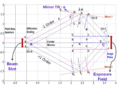
2.2 Reduction Talbot Specific Derivations
Using the nomenclature shown in Fig. 2.5, important relationships between the set
up parameters are derived for the reduction Talbot design such as diffraction angle, beam
size, and mirror tilt angle with output parameters such as interfering angle, pattern pitch,
exposure field size, and optical path differences across the field. Beam divergence is
excluded in these calculations.
In Fig 2.5, the first order diffraction angle is denoted as θ, which can be calculated
from illuminating wavelength (λ) and grating pitch (pgrating) as follows
[image:50.612.112.563.349.678.2]
(2.22)
The mirror tilt is denoted as α and the angle between the normal of mirror and the
diffraction order impingent upon it is denoted as β. The relationship between θ, α, and β
can be calculated from the triangle KDE1 as
(2.23)
The beam size is defined as |AC|, which is also equal to |E1L|. Using the law of
sines for E1LG1 triangle
| |
| |
| |
(2.24)
and from (2.24), the relationship between the beam size and its projection along the tilted
mirror can be defined as
| | | | | | | | (2.25)
The interfering angle ( can be calculated from BIF2 triangle as
(2.26)
By using law of sines on E1MG1 triangle, and noting that |HJ| = |G1M|
| |
| |
| |
(2.27)
and from (2.27), the relationship between the exposure field size |HJ| and its projection
along the tilted mirror can be defined as
From (2.28), by using (2.25) for |E1G1|, we can derive the relationship between
the exposure field size and beam size as given in equation (2.29). The field size defined
here actually corresponds to the field length that is in perpendicular direction to the lines.
The field height at the wafer plane will be the same as the input beam height impingent
upon the grating,
| | | | | | | | (2.29)
From (2.29), it can be observed that if mirrors are not tilted (α=0°), exposure field is
equal to the beam size. As the mirror tilt is increased, exposure field gets larger than the
beam size.
The interference pattern pitch is determined by the source wavelength (λ), the
refractive index of the interfering medium (n) and the interfering angle as
(2.30)
The left and right handedness is preserved in the Talbot design. There exists a location at
the image side where two orders completely overlap with each other, which can be
interpreted as the “focal plane” of the IL system. At this location, each point in the image
plane is resulted from the same point source diffracted from the grating. This alleviates
the spatial coherence requirements, if operating at the focal plane [101].
On the other hand, temporal coherence plays a critical role for large field IL
printing. This strongly relates to the spectral width of the excimer laser and its coherence
length. The reduction in image contrast is a result of the “beating” phenomenon. The
corresponding to each wavelength away from each other; as moved away from the field
center. Eventually, summation of these intensity values will wash away the fringes and
contrast will reduce to zero. Some type of wavelength dispersive optical elements such
etalons, diffraction gratings, or prisms can be introduced in the resonating chamber in
order to narrow down the spectral line to picometer levels [101].
Even with line narrowing, the high contrast region is still on the order of few
millimeters. The beating frequency, which defines useful image area, is related to the
source temporal coherence length and set up parameters. Lowering the beating frequency
increases the useful imaging area and increases the beating period, L. If mirrors in the
Talbot design are not tilted, wavelength dependence on pattern pitch is eliminated and the
system becomes achromatic [101].
For chromatic IL systems, temporal coherence length (lc) of the laser is very
important. It depends on the mean wavelength (λ) and the source bandwidth (Δλ) as [21]
⁄ (2.31)
A 193 nm laser source with a spectral width of 0.5 pm will have a coherence length of
about 75 mm. Considering the maximum field size defined in ITRS is 26 mm by 33 mm,
this coherence length might suffice for large field applications. However, there will be
2.2.1 Effect of OPD on field size
Aside from beating, another factor that reduces the contrast in reduction Talbot
design with tilted mirrors is the optical path difference (OPD) between two diffraction
orders. It can easily be understood by looking at the problem in Fourier perspective [108],
[image:54.612.115.549.219.430.2]as shown in Fig. 2.6.
Figure 2.6: Effect of optical path difference (OPD) on interference of correlated wave
groups (modified from[108]).
When the mirrors are tilted, +1 and -1 orders will travel different path lengths.
The difference will increase as the distance away from the field center is increased. If a
source point diffracting from the grating is assumed to be composed of several wave
groups, as long as the OPD between the orders is less than the temporal coherence length,
correlated wave groups will interfere with each other at the image plane. If the OPD is
plane to interfere at the same time and their ability to constructively and destructively
interfere will be much reduced [108].
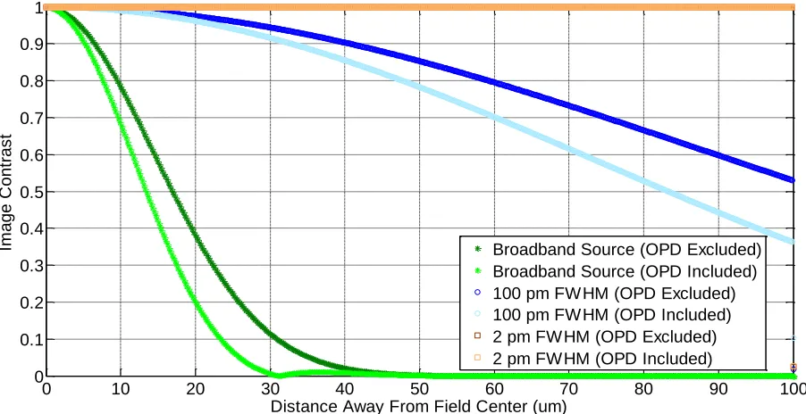
Fig. 2.7 shows the degradation of image contrast when moving away from field
center both due to beating and OPD. For large IL fields, need for a line narrowed laser is
evident from the figure. OPD increases the rate of contrast degradation in addition to the
beating effect. The theoretical derivation of OPD for reduction Talbot design based on set
up parameters is given in Appendix A. It should be noted that the mirror tilt has a strong
[image:55.612.109.560.318.550.2]effect on OPD.
Figure 2.7: Effect of OPD and source bandwidth (i.e. beating) on image contrast
degradation across the field for 193 nm ArF laser. Three different source bandwidths are
considered: broadband, 100 pm FWHM, and 2 pm FWHM.
0 10 20 30 40 50 60 70 80 90 100
0 0.1 0.2 0.3 0.4 0.5 0.6 0.7 0.8 0.9 1
Distance Away From Field Center (um)
Im age C ont ras t
2.3 Line Edge Roughness (LER)
LER is defined simply as the sidewall deviations of a printed line from a straight
line fit [109]. There are several contributors to LER such as chemical/optical shot noise,
random nature of acid diffusion, development process, and concentration of acid
generator/base quencher [18, 19, 110]; but, they can be divided into two categories as:
(1) Chemical properties and processing of the resist related, and
(2) Aerial image related (containing optical properties of the mask and stepper).
It can be measured as a single 3σ value; however, power spectral density (PSD)
is a better metric to distinguish the contribution of different roughness frequencies on the
overall LER [19, 98]. The specifications for LER is usually about 5% of the nominal CD
value; however, LER values of 4 nm and larger are very common [111].
ITRS defines the LF LWR requirements, as shown in Table 2.2 [32]. By 2015, LF
LWR of less than 1.8 nm is demanded from the process. Such low LER/LWR values are
extremely difficult to achieve with state of the art resist/processing techniques.
Table 2.2: 2011 Edition ITRS LWR requirements (generated from data of [32])
Production year 2011 2013 2015 2017 2019 2021
DRAM hp (nm) 36 28 23 18 14 11
Low frequency LWR (nm, 3σ) 2.8 2.2 1.8 1.4 1.1 0.9
In reference [110] a proposed framework for LER/LWR modeling is given as in
related contributors, and the bottom group consists of optical effects, mask roughness and
others that do not belong to the first group [110].
As far as resist-internal LER sources are concerned, the first one is the stacking of
finite size molecules, which gives a white noise spectrum. However, the amplitude can be
ignored because its contribution is mainly in high frequency range which is filtered out in
the processing. Random absorption of photons gives a white noise spectrum, which also
![Figure 1.2: Lithography exposure tool potential solutions for MPU and DRAM [32].](https://thumb-us.123doks.com/thumbv2/123dok_us/41973.3614/26.612.110.535.71.354/figure-lithography-exposure-tool-potential-solutions-mpu-dram.webp)
![Figure 1.3: Process flows for DE, DP, and SP approaches [32].](https://thumb-us.123doks.com/thumbv2/123dok_us/41973.3614/27.612.113.538.163.397/figure-process-flows-dp-sp-approaches.webp)
![Figure 1.8: Different IL setups utilized in literature (reproduced from [85]).](https://thumb-us.123doks.com/thumbv2/123dok_us/41973.3614/34.612.139.502.70.362/figure-different-il-setups-utilized-literature-reproduced.webp)
![Figure 2.6: Effect of optical path difference (OPD) on interference of correlated wave groups (modified from[108])](https://thumb-us.123doks.com/thumbv2/123dok_us/41973.3614/54.612.115.549.219.430/figure-effect-optical-difference-interference-correlated-groups-modified.webp)