Abstract—Spike timing dependent plasticity (STDP) forms the basis of learning within neural networks. STDP allows for the modification of synaptic weights based upon the relative timing of pre- and post- synaptic spikes. A compact circuit is presented which can implement STDP, including the critical plasticity window, to determine synaptic modification. A physical model to predict the time window for plasticity to occur is formulated and the effects of process variations on the window is analysed. The STDP circuit is implemented using two dedicated circuit blocks, one for potentiation and one for depression where each block consists of 4 transistors and a polysilicon capacitor. SpectreS simulations of the back-annotated layout of the circuit and experimental results indicate that STDP with biologically plausible critical timing windows over the range 10µs to 100ms can be implemented. Also a floating gate weight storage capability, with drive circuits, is presented and a detailed analysis correlating weights changes with charging time is given.
I. INTRODUCTION
ignificant research over the last two decades has been undertaken on studying biological neural networks. Specifically this research has focused on how neural networks learn and adapt to their ever changing environment together with the translation of this into biologically inspired hardware neural networks [1-2]. A neural network (NN) consists of interconnecting neurons, with each neuron connecting to another via a synapse. Within the human brain there are in excess of 1011 neurons, with each one having up to 103 synaptic connections [3].
In a NN, the effect that one neuron has upon another will vary depending upon input stimuli and synaptic weight. The synapse is responsible for adaption and learning within a NN [4], through long term potentiation (LTP) or long term depression (LTD), depending on the temporal ordering of the pre- and post-synaptic spikes. Additionally weight modification can also be a short term potentiation (STP) or a short term depression (STD).
Hebb’s theory [5] describes how the synaptic weight is allowed to change based upon the inputs and outputs of each neuron within the NN. A further development of the Hebbian learning concept was the introduction of spike timing dependent plasticity (STDP) in 1983 [6]. STDP is concerned with increasing or decreasing the weight of a synapse based upon the relative timings of pre- and post-synaptic spikes. In biology two STDP functions are commonly reported and referred to as symmetric and asymmetric [4, 6-12]. In this paper we focus on asymmetric STDP as this type of plasticity is known to occur more frequently in biological NN, [4, 7, 11-12]. It is also worth noting that the exponential functions commonly depicted, are not a pre-requisite for STDP but rather a mathematical convenience. What is important however is the relative timings between pre and postsynaptic spikes as this temporal ordering dictates whether potentiation or depression occurs [46, 47]. In asymmetric STDP, weight potentiation (a pre-post spiking event) occurs if a pre-synaptic spike precedes the post-synaptic spike and this leads to LTP; ∆ts is positive. Likewise, the weight is decreased if a post-synaptic spike occurs prior to a pre-synaptic spike, giving rise to LTD (a post-pre spiking event, ∆ts is negative). The critical timing window [7, 18] typically occurs over the range 10-100msec and outside of this window, no potentiation or depression will occur [7, 14-20]. The critical timing window is implemented in this work and is programmable.
It has been shown that STDP can be implemented in hardware, and while the majority of these circuits are biologically plausible, their footprints are large [21-30] requiring up to and, in some cases, exceeding thirty MOSFETs. Other solutions require dedicated microprocessors. A key requirement of hardware neural networks (HNN) is that they are scalable and therefore the designs for neurons, synapses and synaptic modification circuits must be compact, low-powered, while at the same time maintain biological plausibility.
It is proposed here that an STDP circuit with critical time window can be implemented using two dedicated circuit blocks each consisting of 4 MOS transistors, and a polysilicon capacitor. The paper is organized as follows; in section II an overview of theoretical operation of the compact STDP circuit is presented. Section III presents experimental and simulation results undertaken in AMS 0.35µm CMOS process and SpectreS in the Cadence environment respectively. All simulations are conducted on back-annotated layouts, thus incorporating all parasitic elements. A discussion of results relating to the circuit properties is presented in section IV and conclusions drawn in section V.
II. CIRCUIT OPERATION
This section provides an overview of the operation of the proposed STDP weight potentiation and depression circuits. Also
A Compact Spike-Timing-Dependent-Plasticity Circuit for Floating
Gate Weight Implementation
A. Smith, L. McDaid and S. Hall
II.A WP and WD Circuits
The WP circuit is presented in Fig. 1(a) of negative charge stored on the floating gate ( equivalent capacitance CFG. The weight increase occurs
the WP block except that the pre and post spike input terminals are swapped. The WD circuit by removing charge on the FG during a post
Fig. 1 (a) WP and (b) WD circuit
The WP and WD circuits each consist of 3 NMOSTs, M Transistor Mreset is used to ensure that, V
and VPre are high, Mreset is off and will not The initial conditions when no pre- or post by Mleak and C is discharged.
Consider a pre-post spiking event where VTMpre is the threshold voltage of Mpre. When a rate determined by voltage Vleak. Voltage in order to cause the synaptic weight to be and Vwi, are connected and Vwi is pulled up to The synaptic weight will be increased, while
The WP output buffer is constructed using two CMOS inverters with 3 MOSFETs are sized so as to produce the following operation; if inverter then the output from the second inverter,
CMOS inverter, then the output from the second inverter is held at ground. determines how much charge is injected and stored on the FG.
→ min τcg. Finally for a post-pre spiking event of when the presynaptic occurs.
The operation of the WD block is similar to that of the WP block
weight. The WD output buffer is constructed using a single CMOS inverter with 1(b). The inverter MOSFETs are sized so as to produce the following operation; voltage, the output of the buffer is pulled down to
output is 0V. For the case of pre-post spiking, the pre update of the synaptic weight. It should be noted that if
then ∆w = 0 because both the WP and WD circuits will be ‘on’ during this event causing node This is consistent with biophysical experiments where it has been reported [
pre- and post-synaptic neurons is inherently delayed by axons or dendrite latencies and thus the actual strongest and weakest synapse efficacy does not occur at the absolute temporal difference (
(a). The circuit will cause an increase of the synaptic weight by increasing the amount the floating gate (FG) of a non-volatile memory device. This
. The weight increase occurs during a pre-post spiking event. The WD circuit the WP block except that the pre and post spike input terminals are swapped. The WD circuit
ng a post-pre spiking event.
ircuit block with FG device and driver buffer circuit. Voltages indicated are relative to ground.
consist of 3 NMOSTs, MPre, MPost and Mleak, a PMOST, M Vwi and Vwd are pulled low in the absence of VPost and V will not significantly affect Vwi or Vwd. The operation of the WP c
or post- synaptic spikes occur are that Vwi, Vpre and Vpost
post spiking event where a pre-synaptic spike (VPre), increases VC to its maximum value (= When the pre-synaptic pulse ends, C starts to discharge via M
Voltage Vleak thus controls the timing window in which a post to be increased. When the post-synaptic spike (VPost) occurs
is pulled up to VC -VTMpost(Vwi); VTMpost(Vwi) is the threshold voltage associated with M , while Vwi is greater than the trigger voltage of the output buffer
The WP output buffer is constructed using two CMOS inverters with 3.3V and 10V VDD rails, as shown in F
MOSFETs are sized so as to produce the following operation; if Vwi is greater than the trigger voltage of the first CMOS inverter then the output from the second inverter, VCG, will be pulled up to 10V. If Vwi is below the trigger voltage of
then the output from the second inverter is held at ground. The pulse-width, determines how much charge is injected and stored on the FG. As ∆ts→∆ts min, τcg → max τcg
pre spiking event no update of the synaptic weight occurs since V The operation of the WD block is similar to that of the WP block, with post-pre spiking
WD output buffer is constructed using a single CMOS inverter with 3.3V and -10V supply . The inverter MOSFETs are sized so as to produce the following operation; when Vwd
voltage, the output of the buffer is pulled down to -10V. If Vwd is less than the threshold voltage of the inverter, then the post spiking, the pre-synaptic spike causes VC and Vwd to be pulled low and there is It should be noted that if ∆ts = 0 (a pre- and post-synaptic spike occurring at the same time)
w = 0 because both the WP and WD circuits will be ‘on’ during this event causing node
biophysical experiments where it has been reported [50, 51] that synaptic communication between synaptic neurons is inherently delayed by axons or dendrite latencies and thus the actual strongest and weakest
does not occur at the absolute temporal difference (∆ts = 0).
The circuit will cause an increase of the synaptic weight by increasing the amount his device is represented by its The WD circuit is identical to that of the WP block except that the pre and post spike input terminals are swapped. The WD circuit decreases the synaptic weight
and driver buffer circuit. Voltages indicated are relative to ground.
, a PMOST, Mreset and a MOS capacitor, C. and VPre respectively. When Vpost The operation of the WP circuit is now outlined.
are low, node VC is pulled low
its maximum value (= 3.3V-VTMpre): to discharge via Mleak, and VC decreases at ndow in which a post-synaptic spike must occur occurs, the nodes with voltages VC the threshold voltage associated with Mpost. is greater than the trigger voltage of the output buffer.
rails, as shown in Fig. 1(a). The is greater than the trigger voltage of the first CMOS is below the trigger voltage of the first width, τcg, and magnitude of VCG
cg. Similarly as ∆ts→∆ts man, τcg
II.B Critical Timing Window
The critical timing window (CTW) is crucial in biology because it determines the time window over which synaptic modification can occur and is typically 20-25ms for potentiation and depression [7, 9]. However, in hardware the computational speed is greatly accelerated, with average spike train frequencies in the MHz range. We therefore implement an equivalent timing window of 20-25µs in this work although, as will be shown, the window can be programmed to accommodate a wide temporal range. We define here, the critical timing window, tcw, as the time it takes for VC to fall from 90% to 10% of its initial value for both the WP and WD blocks. The rate at which the sub-threshold current reduces VC is set by Vleak and the aspect ratio of Mleak, SMleak. The sub-threshold current, Ileak is constant for VDS = VC > 3kT/q;
= − 1
!
" (1)
where Vt is the threshold voltage of Mleak, q is the charge of an electron, k is the Boltzmann constant and T is absolute temperature. The sub-threshold slope parameter, m = 1 + Cd /Co with Cd being the depletion layer capacitance, Co is the capacitance of the oxide per unit area and µeff is the effective channel mobility. The dynamic operation of the capacitor charging is governed by d# = − $
%&', with Ileak given by Eqn.(1). Performing the integration with voltage limits, 0.9VM
and 0.1VM gives equation (2) which can be used to determine the critical timing window, tcw: VM (= 3.3V-VTMpos) is the maximum value of VC. The window can be adjusted using Vleak according to:
#()= 0.8%$- (2)
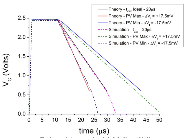
Substituting equation (1) into (2) and rearranging allows a value for Vleak to be calculated for the required tcw. In this study, tcw is chosen to be 20µs, giving Vleak =410mV.
The important effects of process variation upon the critical timing window are now considered. Process variation can affect most parameters of the MOSFET and these can conveniently be represented by the transconductance factor (β) and threshold voltage, Vt [31-43]. Subthreshold MOSFETs are particularly sensitive to process variation because of the exponential relationship between drain current and gate voltage (equation 1). The threshold voltage is also strongly related to several device parameters which are prone to variation during the fabrication process.
For Mleak operating in subthreshold, only Vt is considered, [35, 38, 43-44] as this incorporates variations in both off-current and subthreshold slope, as shown in equation (3), for an n-channel device, where Na is the acceptor doping concentration, tox the oxide thickness, ./ the Fermi potential, Φ1 the work function difference, Qt the trapped oxide charge density, Co the oxide capacitance and ε0, εs, εox are the permittivity of free space, relative permittivity of silicon and silicon dioxide respectively.
'23= #455786 9:5=;56 <+ 2./+ Φ1+@$7! (3)
The variation in '2= '23± ∆'2where Vt0 is the nominal threshold voltage for the AMS process, Vt0 = 0.48, and ±∆Vt is the change in Vt due to process variations. For the AMS process ∆Vt = ±17.5mV. A simple model for the effect of process variation on tcw, can therefore be written as:
∆#() =%=4D E 3.C-$
FG H!=±∆!I
(4)
Fig. 2 tcw variation (max, min and ideal) for Vleak = 400mV.
The effects of process variation on tcw is presented later where it will be shown (Fig. 19) that this variation can be offset by adjusting the learning duration.
III. RESULTS AND DISCUSSION
Simulation and experimental results for the WP block under post-pre spiking conditions are presented in section III.A. Simulated results for the WD block under post-pre spiking conditions are presented in section III.B In both sections III.A and III.B, Vleak is set to 410mV, C is 100fF (4.7µm x 4.7µm) and SMleak = 1 giving tcw = 20µs from equation (5). Additional parameters for the circuit are; WMpre = LMpre = 0.5µm, WMreset = LMreset = 0.5µm, WMpost = 0.4µm LMpost = 0.35µm.
III.A WP Results
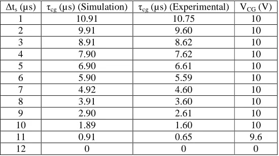
Fig. 3(a) presents simulation and measured results of a post-pre spiking event, where the pre-synaptic spike occurs 5µs after the end of the post-synaptic spike, ∆ts = 5µs. In this case no weight update occurs. This is because C is initially discharged with VC = 0V due to the occurrence of the post spike before the pre spike. Results are now presented in Fig. 3(b), Fig. 4 and Table 1, for a series of pre-post spiking events where the time difference, ∆ts, between pre- and post- synaptic
Fig. 3 – (a)
Fig. 4 (a) Pre
(a) Post-Pre Spiking Event - ∆ts = -5µs (b) Pre-Post Spiking Event - ∆t
Pre-Post Spiking Event - ∆ts = 7µs (b) Pre-Post Spiking Event - ∆ts = 11µs ∆ts = 1µs
In Fig. 4(a), ∆ts is increased to 7µs, again VCG is pulled high to 10V. However τcg is reduced compared to ∆ts =1µs, τcg is
now 4.92µs (simulated) and 4.60µs (measured). The reduction in τcg occurs because Vpost coincides with the linearly decreasing VC. Voltage Vwi now tracks the decreasing VC, until, eventually Vwi is pulled below the trigger voltage of the first CMOS inverter, while Vpost is still high, Fig. 4(a). Finally in Fig. 4(b) ∆ts = 11µs further reduces τcg to 0.91µs and 0.65µs for simulation and measured respectively. The magnitude of VCG is slightly reduced to 9.6V. This corresponds to the minimum weight update ∆w = ∆wmin.
Table 1 presents the results of increasing ∆ts on τcg for both simulation and experimental results. Table 1 indicates that once ∆ts≥ 12µs then no update in the synaptic weight takes place as VCG≈ 0 due to Vwi being less the threshold voltage of the first CMOS inverter when Vpost is high. The results presented in Table 1 represented the upper left hand quadrant of the STDP curve presented later in Fig. 6.
∆ts (µs) τcg (µs) (Simulation) τcg (µs) (Experimental) VCG (V)
1 10.91 10.75 10
2 9.91 9.60 10
3 8.91 8.62 10
4 7.90 7.62 10
5 6.90 6.61 10
6 5.90 5.59 10
7 4.92 4.60 10
8 3.91 3.60 10
9 2.90 2.61 10
10 1.89 1.60 10
11 0.91 0.65 9.6
[image:6.595.161.436.222.376.2]12 0 0 0
Table 1 Effect of positive ∆ts on τcg and VCG
III.B WD Results
As the WD circuit block is identical to the WP circuit with the exception of the application of Vpre and Vpost its operation is also identical. Fig. 5(a) presents simulation and measured results of a pre-post spiking event, where the post-synaptic spike occurs 5µs after the end of the pre-synaptic spike, ∆ts = 5µs. In this case no weight update occurs. Table 2 present the simulation results for a series of post-pre spiking events upon the WD circuit. |∆ts| is once again increased from 1µs to 15µs. Referring to Fig. 5(b), ∆ts = -7µs; as Vpost is pulled high C is charged to voltage VM = 2.43V. As Vpre goes low, C discharges (initially) linearly via Mleak. When Vpre goes high, nodes VC and Vwi are connected such that Vwi≈ 1.70V. A weight decrease is triggered as VCG is pulled down to -10V. Vpre goes low, both Vwi and VCG are pulled back to 0V, ending the synaptic weight update. This is consistent with the theoretical operation outlined previously.
Fig. 5 – (a)
Fig. 6 is a plot of τcg against ∆ts which
from 1µs to 15µs, τcg decreases from 11.31µs to
decreased from -1µs to -15µs τcg decreases from 11.31µs to function since τcg∝ ∆w, where Qinjα∆w.
(a) Pre-Post Spiking Event - ∆ts = 5µs (b) Post-Pre Spiking Event ∆ts =
∆ts (µs) τcg (µs) (Simulation) VCG (V)
-1 11.31 -10
-2 10.92 -10
-3 10.18 -10
-4 9.19 -10
-5 8.14 -10
-6 7.15 -10
-7 6.16 -10
-8 5.15 -10
-9 4.14 -10
-10 3.12 -10
-11 2.06 -10
-12 0.96 -9.6
-13 0.53 -9.6
-14 0 0
Table 2 Effect of negative ∆ts on τcg and VCG
which represents the full STDP curve, shown as the insert.
decreases from 11.31µs to ≈1µs (simulation), from 10.75µs to ≈0.65µs (measured).
decreases from 11.31µs to ≈0.5µs (simulation). This behaviour is characteristic of the STDP w. Note -τcg indicates a reduction in the synaptic weight.
= -7µs
represents the full STDP curve, shown as the insert. Note that as ∆ts is increased ≈0.65µs (measured). Similarly as ∆ts is
Fig. 6 STDP curve from simulation and experimental results. Insert
IV. PHYSICAL
The STDP circuit is to be used with FG devices, therefore we next consider the sensitivity of the weight charge injection to the FG, in relation to the STDP curve presented in Fig.
the change in the associated weight; Qinj
where K =1.5410 N "7
"78 O ;P K/'
, R
effective mass of an electron in the insulator and
be noted that the constants A, B are strictly for tunneling from a metal contact but are similar to the case of injection from a semiconductor [49] and serve our purpose for illustrating the model and method.
Fig. 7 presents the cross-section of a FG device constructed using a poly
onto the FG, Qinj, can be found from consideration of the current in the thin tunneling oxide, t derive a model to allow the determination of
Fig. 7 Equivalent capacitor diagram of FG device, C
of the tunneling oxide. VCG and VFG are the voltages applied to the control gate and coupled onto the FG respectively.
constructed using polysilicon and MOS capacitors. Q
STDP curve from simulation and experimental results. Insert Asymmetric STDP Curve
PHYSICALMODELLINGOFWEIGHTSTORAGE
The STDP circuit is to be used with FG devices, therefore we next consider the sensitivity of the weight charge injection to relation to the STDP curve presented in Fig. 6 and charging time. The charge injected onto the FG
α∆w. The charge is injected by the Fowler-Nordheim mechanism [48].
S/: KT4 UW V78X R 6.8310[9"78
"7 .V
\/ '/], m
o is the mass of an electron at rest, m
effective mass of an electron in the insulator and .V is the barrier height for injection from semiconductor to oxide. It should B are strictly for tunneling from a metal contact but are similar to the case of injection from a semiconductor [49] and serve our purpose for illustrating the model and method.
section of a FG device constructed using a poly-silicon and MOS , can be found from consideration of the current in the thin tunneling oxide, t
ation of Qinj (∆w) and the associated potential of charge stored on the FG, V
Equivalent capacitor diagram of FG device, CFG; CFG = (Cpoly-1+Cox-1)-1 where Cpoly is the capacitance of the interpoly oxide, C
are the voltages applied to the control gate and coupled onto the FG respectively.
constructed using polysilicon and MOS capacitors. Qinj represents the charge stored on the FG and Qrem represents the charge removed from the FG, both due
to FN tunneling.
Asymmetric STDP Curve
The STDP circuit is to be used with FG devices, therefore we next consider the sensitivity of the weight charge injection to and charging time. The charge injected onto the FG Qinj represents
Nordheim mechanism [48].
(5) is the mass of an electron at rest, mox is the
semiconductor to oxide. It should B are strictly for tunneling from a metal contact but are similar to the case of injection from a and MOS capacitor. The charge injected , can be found from consideration of the current in the thin tunneling oxide, tox over a time step, ∆t. We now
w) and the associated potential of charge stored on the FG, V∆w.
is the capacitance of the interpoly oxide, Cox is the capacitance
The capacitively coupled voltage, VFG capacitive coupling coefficient, defined as
it is assumed that there is no parasitic charge in the oxide or initially stored on the FG. is the surface potential at the oxide-semiconductor interface. The field at
equation (6) (see appendix for derivation).
The associated change in potential is calculated by finding the difference between successive steps of field:
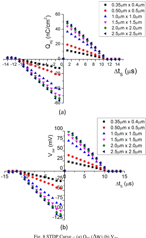
The charge per unit area injected onto the FG for the duration of the pulse width Fig. 8 presents plots of (a) Qinj against
tunneling area. The increment of charge injected decreases for increasing electric field.. Similarly as ∆ts is decreased below
The results indicate that Qinj (and V∆w
Increasing the device tunneling area causes a shift in the STDP curve. Specifically this is a shift in the magnitude of the charge injected/removed for the same ∆t value.
The effect of process variation (PV) on the STDP curves is now cons
FG which falls across tox is shown in Fig. 7, and given by capacitive coupling coefficient, defined as ^ = $_7`
$78a$_7`. The electric field in the oxide, Eox is given
it is assumed that there is no parasitic charge in the oxide or initially stored on the FG. VFG is the potential of the FG and semiconductor interface. The field at successive time steps,
(see appendix for derivation).
T4baO= R cde fg#278hV$=+ UW78VbXij O
The associated change in potential is calculated by finding the difference between successive steps of field: '∆) #4T4k T4k > 1
The charge per unit area injected onto the FG for the duration of the pulse width ∆tis then found as
against ∆ts and (b) V∆w against ∆ts. Fig. 8 (a) presents the STDP curve for increasing tunneling area. The increment of charge injected decreases for increasing ∆t because the stored charge serves to reduce the
[image:9.595.181.415.306.686.2]is decreased below -1µs, the amount of charge removed is also decreased.
Fig. 8 STDP Curve – (a) Qinj(∆w) (b) V∆w
∆w) tracks τcg due to the similar shape of the Qinj (V∆w)
Increasing the device tunneling area causes a shift in the STDP curve. Specifically this is a shift in the magnitude of the
∆t value.
The effect of process variation (PV) on the STDP curves is now considered. Fig. 9 shows the effect of PV upon the output , and given by '/l ^'$l, where α is the
is given as T4<m ;6
278 , where
is the potential of the FG and .n time steps, ∆t, can be found from
(6)
The associated change in potential is calculated by finding the difference between successive steps of field:
(7) then found as ∆o ∝ pbqr 3'∆) . (a) presents the STDP curve for increasing t because the stored charge serves to reduce the
is also decreased.
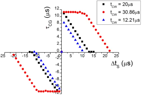
characteristics of the STDP circuit, τcg against ∆ts. The plot concurs with the earlier statement that PV can either increase or decrease tcw. The effect of this is to cause a shift in the ideal τcg against ∆ts curve. If PV causes tcw < tcwideal (20µs) the curve is shifted to the left. Conversely if tcw > 20µs the curve is shifted to the right.
Fig. 9 τcg v ∆ts STDP curves showing effect of process variation (max, min and ideal)
The effect of PV is to vary the amount of charge (hence potential of charge) injected/removed from the FG. For tcw < 20µs
∆w (V∆w) curve is shifted to the left. Conversely if tcw > 20µs ∆w (V∆w) curve is shifted to the right. Specifically there is no overall change in the magnitude of ∆w, Qinj. Rather there is a shift in the magnitude of the charge injected/removed for the same ∆ts value. This does not affect the overall operation of the STDP circuit in that it still follows the STDP rule. However, the amount of charge injected can be compensated for by altering the learning duration.
V. CONCLUSION
Compact STDP circuit blocks have been proposed, which can control weight increase and decrease within a hardware neural network. Simulation and experimental results of the WP circuit are presented which indicate that for a post-pre spiking event, no update of the synaptic weight occurs. A pre-post spiking event will however cause the synaptic weight, which is represented as charge on the FG of the synapse, to be increased. The amount, by which the synaptic weight is changed, ∆w, is determined by the duration that Vwi is greater than 1.2V and by the magnitude of VCG. The maximum weight, ∆wmax is obtained when VCG has a pulse width of ≈11µs and a constant magnitude of 10V. The minimum weight, ∆wmin, prior to Vwi being less than 1.2V is achieved when VCG has a pulse width of 0.9µs and magnitude of 9.6V.
Furthermore, the critical timing window within which synaptic modification takes place can also be controlled with voltage, Vleak. The key issue of the significant influence of process variations for devices operating in subthreshold has been modeled. We show that process variations do not adversely affect the learning dynamics because the weight changes depend on the temporal difference within the STDP window. Also changes in charging/discharging duration can be compensated for within the learning algorithm. Additionally a model correlating charge alterations within the FG as a function of the charging/discharging duration was presented and this relationship was extended to show the dependency of the weight changes on the temporal difference between pre and post synaptic spikes.
ACKNOWLEDGMENT
The work was funded by the Engineering and Physical Sciences Research Council, UK, project reference EP/F05551X.
APPENDIX
Equation 6 is derived as follows. We start with the FN Equation:
S/:= 3ss278= KT4 UW V78X (A.1)
sW78
s2 =
O s2=8
s78
s2 (A.2)
hence
S/:T4 = 3#4sWs278 (A.3)
Separate variables:
S/:T4&# = 3#4&T4= KT4 UW V78X &# (A.4)
3#4hW O
78t4DUv78uPX&T4= &# (A.5)
$=278
h w T4 U
V W78X &T4
W78xyz
W78b = w &#
2baO
2b (A.6)
Where t(i+1) – t(i) = ∆t, the time step. Integrating, putting in limits and re-arranging gives de g#$=hV278+ UW78VbX = {W V
78xyz| (A.7)
And finally,
T4k + 1 = R }de ~g##KR
4 3+ {
R T4k|
O
(A.8)
REFERENCES
[1] G. Indiveri, E. Chicca and R. Douglas, “A VLSI array of low-power spiking neurons and bistable synapses with spike-timing dependent plasticity,” IEEE. Trans. Neural Networks, vol. 17, no. 1, pp. 211-221, 2006.
[2] C. Diorio, P. Hasler, B. A. Minch and C. A. Mead, “A single transistor silicon synapse”, IEEE Trans. Electron Devices, vol. 43, no. 11, pp. 1972-1980, 1996.
[3] D. H. Goldberg, G. Cauwenberghs and A. G. Andreou, “Probabilistic synaptic weighting in a reconfigurable network of VLSI integrate-and-fire neurons”, Neural Networks, vol. 14, pp. 781-793, 2001.
[4] L. F. Abbott and S. B. Nelson, “Synaptic plasticity: taming the beast”, Nature Neuroscience supplement, vol. 3, pp. 1178-1183, 2000. [5] D.O. Hebb. The Organisztion of Behaviour. Wiley 1949.
[6] W.B. Levy and O. Steward, “Temporal contiguity requirements for long-term associative potentiation/depression in the hippocampus,” Neurosience, vol. 8, no. 4, pp. 791-797, 1983.
[7] G.Q. Bi and M.M Poo, “Synaptic modification in cultured hipocampl neurons: Dependence on spike timing, synaptic strength and postsynaptic cell type,” J. Neuroscience, vol. 18, pp. 10462-10472, 1993.
[8] M.Nishiyama, K. Hong, K. Mikoshiba, M.M. Poo and K. Kato, “ Calcium stores regulate the polarity and input specificity of synaptic modification,” Nature, vol. 408, pp. 584-588, 2000.
[9] M. Tsukada, T. Aihara, Y. Kobayashi and H. Shimazaki, “ Spatial analysis of spike-timing-dependent ltp and ltd in the ca1 area of hipocample slices using optical imaging,” Hippocampus, vol. 15, no. 1, pp. 104-109, 2005.
[10] H. Tanaka, T. Morie, and K. Aihara, “A CMOS spiking neural network with symmetric/asymmetric STDP function,” IEICE Transcations on Fundamentals, vol E92-A, no. 7, pp. 1690-1698, 2009.
[11] G.Q. Bi and M.M Poo, “Synaptic modification of corrolated activity: Hebbs postulate revisited,” Annu. Rev. Neurosci, vol. 24, pp. 139-166, 2001 [12] N. Caporale and Y. Dan, “Spike timing-dependent plasticity: A Hebbian learning rule,” Annu. Rev. Neurosci, vol. 31, pp. 25-46, 2008
[13] I. B. Levitand and L. K. Kaczmarek, The Neuron – Cell and Molecular Biology, 3rd Edition, Oxford University Press, 2002
[14] D. Purves, G. J. Augustine, D. Fitzpatrick,. L. C. Katz, A. LaMantina, J. O. McNamara and S. M. Willians, Neuroscience, 2nd Edition, Sinauer
Associates Inc, 2001.
[15] N. Rebola, B. N. Srikumar and C. Mulle, “Activity-dependent synaptic plasticity of NDMA receptors”, J. Physiol, vol. 588, no. 1, pp. 93-99, 2010. [16] S. Song, K. D. Miller and L. F. Abbott, “Competitive Hebbian learning through spike-timing-dependent synaptic plasticity”, Nature Neuroscience, vol.
[17] P. J. Dew and L. F. Abbott, “Extending the effects of spike-timing-dependent plasticity to behavioral timescales”, PNAS, vol. 103, no. 23, pp. 8876-8881, 2006.
[18] R. C. Froemke, D. Debanne and G. Q. Bi, “Temporal modulation of spike-timing-dependent plasticity”, Frontiers in Synaptic Neuroscience, vol. 2, no. 1, pp. 1-16, 2010.
[19] K. A. Buchanan, and J. R. Mellor, “The activity requirements for spike-timing-dependent plasticity in the hippocampus”, Frontiers in Synaptic Neuroscience, vol. 2, no. 11, pp. 1-5, 2010.
[20] Z. F. Mainen and T. J. Sejnowski, “Reliability of spike timing in neocortical neurons”, Science, vol. 268, pp. 1503-1506, 1995.
[21] S J. Schemmel, K. Meier and E. Mueller, “ A new VLSI model of neural microcircuits including spike timing dependent plasticity,” IEEE International Joint Conference on Neural Networks 2004, vol. 3, pp. 1711-1716, 2004.
[22] J. Schemmel, K. Meier and E. Mueller, “Implementing synaptic plasticity in a VLSI spiking neural network model,” IEEE International Joint Conference on Neural Networks 2006, pp. 1-6, 2006.
[23] K. Cameron, V. Boonsobhak, A. Murray and D. Renshaw, “Spike timing dependent plasticity (STDP) can ameliorate process variations in neuromorphic VLSI,” IEEE Transactions on Neural Networks, vol. 16, no. 6, pp. 1626-1637, 2005
[24] A. Bofill-i-Petit and A. F. Murray, “Synchrony detection and amplification by silicon neurons with STDP synapse,” IEEE Transactions on Neural Networks, vol. 15, no. 5, pp. 1296-1304, 2004
[25] Y. Hayashi, K. Saeki, and Y. Sekine, “A synaptic circuit of a pulse-type hardware neuron model with STDP,” International Congress Series, vol. 1301, pp. 132-135, 2007.
[26] K. Saeki, R. Shimizu and Y. Sekine, “Pulse-type hardware neural network with two time window STDP,” ICONIP 2008, Lecture Notes In Computer Science, vol. 5507/2009, pp. 877-884, 2009.
[27] M. M. Khan, D. R. Lester, L. A. Plana, A. Rast, X. Jin, E. Painkras and S. B. Furber, “SpiNNaker: Mapping nerual networks onto a massively-parallel chip multiprocessor,” International Joint Conference on Neural Networks 2008, pp.2850-2857, 2008.
[28] X. Jin, M. Lujan, L. A. Plana, S. Davies, S. Temple and S. B. Furber, “Modeling spiking neural networks on SpiNNaker,” Computing In Science and Engineering, vol. 12, no. 5, pp. 91-97, 2010.
[29] X. Jin, A. Rast, G. Galluppi, S. Davies, and S. B. Furber, “Implementing spike-timing-dependent plasticity on SpiNNaker neuromorphic hardware,” World Congress on Computational Intelligence 2010, pp. 2302-2309, 2010 Markram, H, “The blue brain project,” Nat Rev Neurosci. vol. 7, pp. 153-160, 2006.
[30] Druckmann, S. et al., “A Novel Multiple Objective Optimization Framework for Constraining Conductance-Based Neuron Models by Experimental Data,” Frontiers in Neuroscience, vol. 1, no. 1, 2007
[31] Kozloski, J. et al., “Identifying, tabulating, and analyzing contacts between branched neuron morphologies,” IBM Journal of Research and Development, Vol 52, Number 1/2, 2008
[32] David C. Potts, “Statistical Analog Circuit Simulation: Motivation and Implmentation”, Advances in Analog Circuits, InTech, 2011.
[33] Yuhua Cheng, “The influence and modeling of process variation and device mismatch for analog/RF circuit design”, Proceedings of the 4th IEEE International Caracas Conference on Devices, Circuits and Systems 2002M
[34] .J.M. Pelgrom, A.C.J. Dunimaiker and A.P.G. Welbers, “Matching Properties of MOS Transistors”, IEEE Journal of Solid State Circuits, vol. 24, no. 5, pp. 1433-1440, 1989.
[35] M.J.M. Pelgrom, H.P. Tuinhout and M. Vertregt, “Transistor matching in analog CMOS applications”, IEDM, pp. 915-918, 1998. [36] M.T. Terrovitis and C.J. Spanos, “Process Variability And Device Mismatch”, First International Workshop on Statistical Metrology, 1996
[37] P.G. Drennan and C.C McAndrew, “Understanding MOSFET mismatch for analog design”, IEEE Journal of Solid State Circuits, vol. 38, no. 3, pp. 450-456, 2003.
[38] P.R. Kinget, “Device mismatch: An analog design perspective”, ISCAS 2007, pp. 1245-1248, 2007.
[39] R. Jaramillo-Ramirez, J. Jaffari and M. Anis, “Variability aware design of subthreshold devices”, ISCAS 2008, pp. 1196-1199, 2008.
[40] H. Kosina, M. Nedjalkov and S. Selberherr, “Theory of the Monte Carlo method for semiconductor device simulation”, IEEE Transactions on Electron Devices, vol. 47, no. 10, pp. 1898-1908, 2000.
[41] H. . Hung and V. Adzic, “Monte Carlo simulation of device variation and mismatch in analog integrated circuits”, NCUR 2006, 2006.
[42] J. B. Shyu, G.C. Temes and F. Krummenacher, “Random error effects in matched MOS capacitors and current sources”, IEEE Journal of Solid State Circuits, vol. sc-19, no. 6, pp. 948-955, 1984.
[43] J. B. Shyu, G.C. Temes and K. Yao, “Random error in MOS capacitors”, IEEE Journal of Solid State Circuits, vol. sc-17, no. 6, pp. 1070-1076, 1982 [44] B. Zhai, S. Hanson, D. Blaauw and D. Sylvester, “Analysis and mitigation of variability in subthreshold design”, ISLPED 2005, pp. 20-25, 2005 [45] S. N. Mozaffari and A. Afzali-Kusha, “Statistical model for subthreshold current considering process variation”, ASQED 2010, pp. 356-360, 2010 [46] R. Kempter, W. Gerstner and J.L. van Hemmen, “Hebbian learning and spiking neurons”, Phys. Rev. E, vol. 59, pp. 4498-4514, 1999.
[47] W. Gerstner, R. Kempter, J. L. van Hemmen, and H. Wagner, “A neuronal learning rule for sub-millisecond temporal coding”, Nature, vol. 386, pp. 76-78, 1996.
[48] R.H. Fowler and L. Nordheim, “Electron emission in intense electric fields”, Proceedings of the Royal Society of London A, vol. 119, pp. 173-181, 1928
[49] Z. A. Wienberg, “On tunneling in metal-oxide-silicon structures”, Journal of Applied Physics, vol. 53, no. 7, pp. 5052-5056, 1962
[50] P. D. Roberts and C. C. Bell, “Spike timing dependent synaptic plasticity in biological systems”, Biological Cybernetics, vol. 87, no. 5-6, pp. 392-403, 2002.
[51] B. Lu, W.M. Yamada, and T. W. Berger, “Asymmetric Synaptic Plasticity Based on Arbitrary Pre- and Postsynaptic Timing Spikes Using Finite State Model”, Proceedings of International Joint Conference on Neural Networks, Orlando, Florida, USA, August 12-17, 2007