Chambers, B. and Tennant, A. (2005) A smart radar absorber based on the
phase-switched screen. IEEE Transactions on Antennas and Propagation, 53 (1 (par). pp.
394-403. ISSN 0018-926X
https://doi.org/10.1109/TAP.2004.838795
[email protected] https://eprints.whiterose.ac.uk/
Reuse
Unless indicated otherwise, fulltext items are protected by copyright with all rights reserved. The copyright exception in section 29 of the Copyright, Designs and Patents Act 1988 allows the making of a single copy solely for the purpose of non-commercial research or private study within the limits of fair dealing. The publisher or other rights-holder may allow further reproduction and re-use of this version - refer to the White Rose Research Online record for this item. Where records identify the publisher as the copyright holder, users can verify any specific terms of use on the publisher’s website.
Takedown
If you consider content in White Rose Research Online to be in breach of UK law, please notify us by
A Smart Radar Absorber Based on the
Phase-Switched Screen
Barry Chambers
, Senior Member, IEEE,
and Alan Tennant
, Member, IEEE
Abstract—Although conventional (i.e., passive) radar absorbers are widely used for modifying the radar cross-section (RCS) of current military platforms, such absorbers may not have adequate performance to satisfy future requirements. Active absorbers, however, offer the potential to overcome the so-called Rozanov performance limit and to enable additional smart functionality such as monitoring damage, adaptive control of RCS or target appearance, identification-friend-or-foe, and absorb-while-scan. This paper outlines the concept and basic properties of a novel type of active radar absorber, the so-called phase-switched screen (PSS). The basic PSS topology is then modified so as to enable it to operate as a smart radar absorber when used together with an external sensor and feedback control loop. System implementation issues and the optimum choice of design parameters for a range of operational scenarios are discussed, and theoretical predictions are supported by measured performance data.
Index Terms—Electromagnetic scattering, modulation, radar absorbing material, radar cross-section.
I. INTRODUCTION
A
LTHOUGH conventional (i.e., passive) radar absorbers are widely used for modifying the radar cross-section (RCS) of current military platforms, such absorbers may not have adequate performance to satisfy some future require-ments. For example, a passive radar absorber, once designed and manufactured, has fixed characteristics that are bounded by the electrical thickness at the lowest desired operating wavelength, following the so-called Rozanov limit [1]. Hence if the threat for which the absorber was designed changes, then either reduced performance against the new threat must be accepted or the material must be replaced by a better one. Active absorbers, however, offer the potential to overcome the Rozanov limit and to enable additional “smart” functionality such as monitoring damage, adaptive control of RCS or target appearance, identification-friend-or-foe, and absorb-while-scan [2].Rozanov and earlier authors have shown that there are limita-tions to the performance of a particular absorber configuration and clearly these must apply to both passive and active absorbers since both obey the same laws of physics. However, although an active absorber, in one particular electrical configuration,
is Rozanov-limited, it has the ability to change to a different configuration, which then has a different associated Rozanov limit. Hence an active absorber has the property that the sum of
Manuscript received February 3, 2003; revised May 11, 2004.
The authors are with the Department of Electronic and Electrical Engi-neering, University of Sheffield, Sheffield S1 3JD, U.K. (e-mail: [email protected]).
Digital Object Identifier 10.1109/TAP.2004.838795
itsinstantaneousbandwidths at a given reflectivity level is po-tentially larger than the Rozanov limit for the original passive absorber.
In general, passive and active absorbers rely on either destruc-tive interference or the conversion of incident energy into heat; recently, however, a new type of active “absorber” has been pro-posed, the so-called phase-switched screen (PSS). Rather than absorbing the incident energy as heat, the PSS reflects it and spreads it over a very wide bandwidth using phase modulation. If this is done correctly, very little reflected energy will lie within the receiver bandwidth and thus the PSS exhibits the same be-havior,so far as the receiver is concerned,as would an actual absorber. Although we have reported on a number of planar and conformal PSS configurations [3]–[12], in this paper we will consider only that based on a planar Salisbury screen in which the normal resistive sheet has been replaced by a layer whose conductance can be changed periodically with time in accor-dance with some externally applied electrical or optical stim-ulus. In the context of the discussion that follows, a smart ab-sorber is defined as one that combines the attributes of incident field sensing, feedback, and electromagnetic reconfiguration. In the case of the active Salisbury screen configuration, the key to achieving smartness lies in replacing the perfectly conducting backplane by one that is “leaky.” In this paper, we consider how this concept may be used with a PSS rather than with the other types of active radar absorber discussed previously [2], [13]–[15].
Although several approaches may be used to explain the con-cept and basic properties of the PSS, here we will use that based on a transmission-line analog (TLA) of the absorber structure. This is valid for both continuous-wave and pulsed incident sig-nals since in general the duration of an incident radar pulse is very long compared with the wave transit time through the ab-sorber structure and the time for one-half cycle of the switching waveform used to control the active layer in the absorber. An analysis of the PSS based on the spectral approach is given in [9].
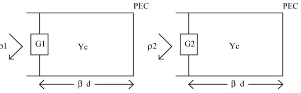
II. BASICTHEORY OF THESINGLE-LAYERPSS
The transmission-line analog of the single-layer PSS is shown in Fig. 1. It consists of a short-circuited length of transmission line with characteristic admittance and propagation constant , across whose input terminals is placed a conductance , defined as
(1)
Fig. 1. Transmission-line analog of the PSS in its two states.
where is theONtime and is the time period for one cycle of the waveform used to control the state of . Depending on the incident polarization and angle of incidence , is given by either for parallel polarization or for perpen-dicular polarization, where is the characteristic admittance of free-space. For either polarization, is given by . Thus, the input admittance of the PSS can assume one of two states—either or —given by
(2)
These result in reflection coefficients and , which are related to and by
and (3)
where or for parallel or perpendicular polarization, respectively. Since and are arbitrary, then
and are generally complex.
For the PSS to behave like a perfect microwave absorber at a particular frequency, then the reflection coefficient , when averaged over time , must be equal to zero, i.e.,
(4)
For the case of ideal square-wave switching, this gives
(5)
which leads to the general admittance relation for the PSS. Thus, from (3) and (5) we have:
(a) parallel polarization
(6)
(b) perpendicular polarization
(7) In the simplest case when , (6) and (7) become
and (8)
or, when written in terms of the switched conductances and :
(a) parallel polarization
(9)
(b) perpendicular polarization
(10)
If the incident frequency is such that , then and (9) and (10) simplify to
and (11)
respectively. Since the time-averaged reflection coefficient is zero, the PSS behaves like a perfect absorber at , as expected. When , will not in general be equal to zero but for the special case when and , it is easy to show that varies as . The more general case for oblique incidence is discussed elsewhere [8].
Hence, when , (11) gives the required relationship between the resistances of the PSS active layer in its two states, i.e.,
(12)
where , , and .
Equation (12) was derived independently for active radar ab-sorbers in [4], but it has been reported previously in connection with diode-switched reflection phase shifters [16]. Although not mentioned in the literature, (12) also applies to the passive Sal-isbury screen, since it relates the two possible values of front sheet resistance which give a particular reflectivity null depth.
, and the time-averaged value of as expected, since the “on” time was chosen to equal T 2.
As mentioned above, when , then varies as . Thus the bandwidth of the PSS is somewhat narrower than that of the Salisbury screen [9], and this behavior may be explained by considering the influence of multiple reflections inside the PSS structure. When and , the incident wave is only reflected from either the front or the back face of the PSS and no multiple reflections can occur. For other combinations of and , however, some of the wave incident on the front face of the PSS can always penetrate into its interior, thus giving rise to multiple reflections which will change the frequency characteristics. In the limiting case, when then the frequency characteristics of the PSS become identical to those of the ideal Salisbury screen.
As we have seen, at resonance (i.e., ), the effect of switching between values and , as related by (11), mimics the reflectivity characteristics of a passive layer having a sheet resistance equal to . Hence it should be possible to adjust the effective sheet resistance by varying the “on” time in each switching cycle. The relationship between and is given by [4]
(13)
Thus the PSS may be configured to act as a reflector or as a variable absorber simply by changing the duty cycle of the switching waveform applied to the active layer.
III. EVOLUTION OF THESMARTPSS STRUCTURE
For the PSS to be made smart, it is necessary to modify its structure so as to facilitate two key requirements: incident field sensing and electromagnetic reconfiguration. Specifically, what we have in mind is a structure based on the PSS that has the ability to sense the frequency of an incident wave and to auto-matically place a reflectivity null of chosen depth onto that fre-quency so as to modify the target’s electromagnetic appearance to the incident wave. As mentioned before, the first requirement, that for incident field sensing, may be facilitated by making the PSS backplane “leaky” and by incorporating some form of fquency measuring element into the structure. The second re-quirement can be fulfilled by increasing the number of active layers in the PSS, thereby enabling simultaneous null depth and position control.
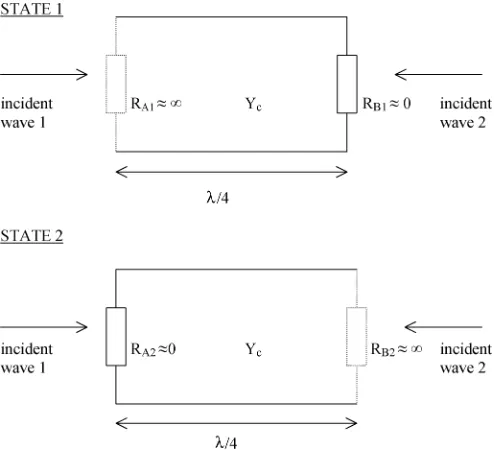
The first stage in the evolution of the smart PSS was the realization that the backplane could also be made active. The resulting bidirectional PSS (BPSS), shown in Fig. 2, is effec-tive against illumination from either side of the structure and could thus be used in applications where the latter is electrically thin (e.g., a missile fin). In operation, the two active layers are switched in antiphase so that during a particular half-cycle of the switching waveform, , , whereas during the next, , , and so on. Then, irrespec-tive of the value of , the BPSS will have the same apparent reflectivity when viewed from either side (see [10, Fig. 4]).
[image:4.594.305.552.64.289.2]In a previously reported implementation of a self-tuning radar absorber [2], [12], [13], sensing of the incident frequency was
Fig. 2. Bidirectional phase-switched screen in its two operating states.
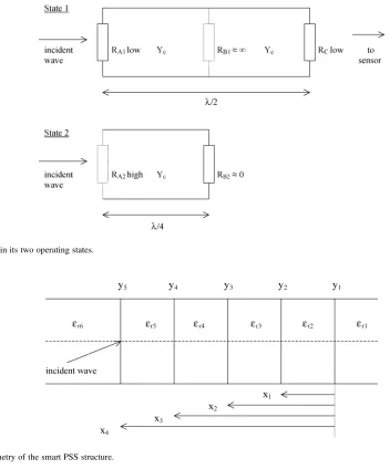
achieved by adding a tunable 2 resonator section behind the absorber backplane (which was partially transparent). Although effective, this resulted in a structure that was 3 4 thick. When applying this technique to the PSS, however, it was realized that the 4 thickness of the PSS is only used for half the time (i.e., when the active front layer resistance . When , the structure behind the active front layer can be used as one-half of the 2 resonator section, as shown in Fig. 3(a). This results in a total structure thickness of only 2 but does require so as to ensure that a small sample of the incident signal can pass through the 2 resonator section and be detected. Since the general structure of the smart PSS, as shown in Fig. 3, is more complex than that of the single-layer PSS, shown in Fig. 1, (12) now relates the input resistances of the smart PSS in its two states, rather than the two values of the active layer resistance. Working in terms of rather than , for simplicity, and are now related by
(14)
where represents the loading of the PSS structure caused by the sensor at the output end of the 2 resonator section. Since must be positive, this places restrictions on the values of the quantities appearing in (14), but in practice the latter will be
satisfied if (e.g., )
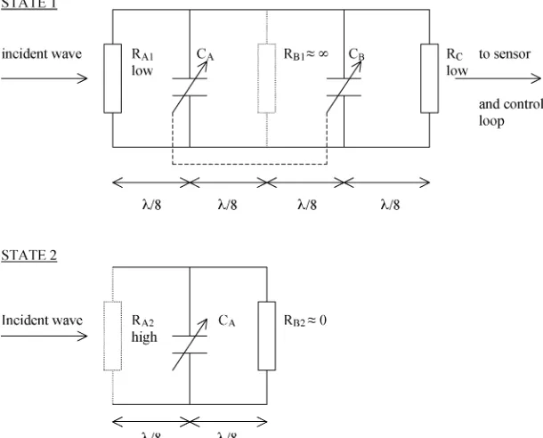
In summary, therefore, the final smart PSS structure is 2 thick at the incident frequency and operates alternately in one of two states. In State 1, shown in Fig. 3(a), the resistance of the active front layer is typically a few and the active layer defining the PSS backplane has a high resistance (several tens of k ). For simplicity, the value of the back resistive layer
[image:4.594.334.552.531.599.2]Fig. 3. Smart PSS in its two operating states.
Fig. 4. Layer geometry of the smart PSS structure.
Q factor and insertion loss are determined by the value of . In State 2, shown in Fig. 3(b), is switched to a high value, determined from (14), and is set low . In this state, is left at its original value so as to ensure that transmission through the structure is low.
In the next section, we present a general analysis of the smart PSS structure and then use this to verify its reflection and trans-mission characteristics versus frequency.
IV. GENERALTHEORY OF THESMARTPSS
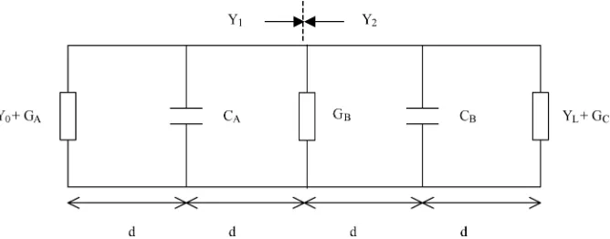
[image:5.594.141.452.65.289.2]In this section, the smart PSS structure shown in Fig. 3 is generalized to include provision for reactive tuning elements. The resulting structure, shown in Fig. 4, is composed of five distributed sheet admittances , sandwiched between six dielectric layers, the first and last of which are assumed to be semi-infinite regions. The microwave reflection and transmis-sion coefficients of this dielectric stack for arbitrary incidence angles and polarizations are readily obtained using multilayer stepping theory [17]. This involves the repeated use of the gen-eral transformer relationships between the incident, reflected, and transmitted wave amplitudes at the interface between the
Fig. 5. Admittance sheet sandwiched between two dielectric layers.
th and th layers, as shown in Fig. 5. The required equations for perpendicular incident polarization are
[image:5.594.317.534.494.626.2]and
(16)
and those for parallel incident polarization are
(17)
and
(18)
where is the admittance of an impedance (R or C) sheet placed between the th and th layers in the stack is the location of the th interface, and and are the angles of incidence and refraction at the th interface. The characteristic admittances of the th and th layers in the stack and will be determined by the layer parameters and together with the values of and . Equations (15) and (16) or (17) and (18) are used iteratively to find and at the front of the stack (i.e., the PSS front face) from arbitrarily chosen starting condi-tions at the back of the stack, namely, , (i.e., the sensor is matched).
The structure reflection coefficient is then defined in terms of and as
(19)
and the transmission coefficient through the structure is given by
(20)
To determine the time-averaged reflectivity of the PSS, (19) is used to determine for the structure in its two states. These are then combined using (5), i.e.,
Reflectivity dB (21)
where
(22)
Similarly, the time-averaged insertion loss of the 2 res-onator is given by
Insertion Loss dB
[image:6.594.311.551.68.244.2](23)
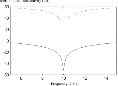
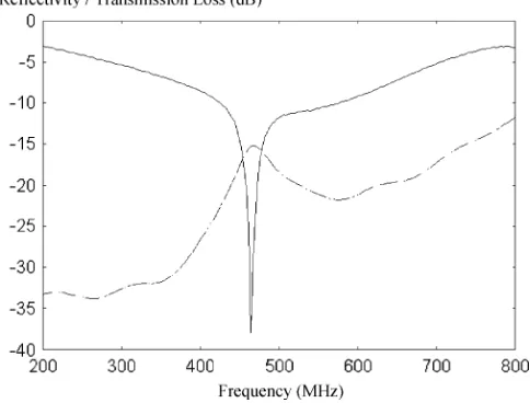
Fig. 6. Reflectivity and insertion loss characteristics of fixed-tuned smart PSS R = R = 10 ,R = 1 M,R = 28 380 ,R = 1 , d = 7:5mm insertion loss, reflectivity.
As a check on the validity of the above theory, (21)–(23) were used to calculate the frequency characteristics of an ideal fixed-tuned smart PSS structure in free-space which was 15 mm thick (i.e. 2 at 10 GHz with spacer ) and with
, , , , and
. As can be seen from Fig. 6, the curves of reflectivity and insertion loss have the desired characteristics, with a deep reflectivity null and minimum insertion loss both occurring at the desired frequency. In the next section, we consider how best to tune the smart PSS and the optimum choice of (and hence ).
V. SYSTEMASPECTS
A. Smart PSS Tuning
Fig. 7. Tunable smart PSS structure in its two operating states.
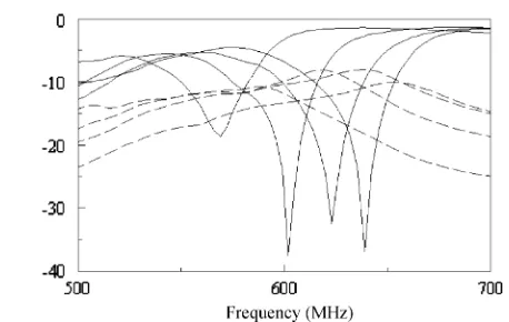
Fig. 8. Tuning and tracking characteristics of smart PSS C = C = 0 fF, solid lines are forC = C = 50; 100;and200fF, respectively.
resonator now being in length. When , two fea-tures in the curves are apparent. First, the reflectivity null and minimum insertion loss frequencies do indeed track correctly, but the second resonance point in the insertion loss curve has moved much closer to the fundamental resonance point. This has occurred since the tuning capacitors are at the ideal posi-tions for tuning the resonator at its second harmonic, rather than at the desired fundamental frequency. This should not cause any problems, however, since the two resonances are still well sep-arated for any values of capacitance that are likely to be used in practice.
The above discussion has assumed that the incident wave is normal to the PSS front face. For the case of oblique incidence, however, correct frequency tracking between the PSS and the resonator will still occur since the electrical length of both struc-tures is defined similarly in terms of . A discussion of how the
Fig. 9. Behavior of smart PSS in absorb-while-scan mode solid lines are for C = C = 50fF, C = 0fF, C = 100fF.
PSS should be switched so as to be effective against both inci-dent polarizations simultaneously is given in [8].
B. Absorb-While-Scan Mode of Operation
In Section V-A, we considered the behavior of the smart PSS when the two tuning capacitors and had the same value. In a given situation, once the PSS reflectivity null has been tuned onto a threat frequency , it is possible to keep fixed (so as to keep the reflectivity null at ) and to tune the resonator
independentlyby changing the value of , as shown in Fig. 9. By this means, the smart PSS structure may be used to search for a second threat frequency while simultaneously dealing with the first; this mode of operation is termedabsorb-while-scan.
If a second threat frequency of higher priority is found when , the PSS reflectivity null may be retuned to this by
[image:7.594.308.550.353.529.2]Fig. 10. Calculation of resonance conditions for absorber and resonator sections of the smart PSS structure.
be determined using the transverse-resonance technique [18]. Starting with the equivalent circuit of the smart PSS in State 1, as shown in Fig. 7, the resonator is assumed to be terminated at its input by a parallel combination of and and at its output by a parallel combination of and , as shown in Fig. 10. Then we may equate the local admittances and seen on either side of some arbitrary reference plane within the resonator. This leads to a general equation that gives the resonant frequency
, for known values of and (since in general ). When the reference plane is positioned at the center of the resonator, we obtain
(24)
where
(25)
(26)
and .
may then be substituted back into (24) to find the value of two new identical capacitors and , which will again tune the resonator to . It is the new capacitor that is then used to position the PSS reflectivity null at the new threat frequency
.
As an example, if , ,
, , and mm, then from
[image:8.594.316.551.230.401.2](14), . Let the initial threat frequency GHz; then from (24), the PSS absorber and resonator sec-tions can be tuned to this by setting . If a new threat now occurs at frequency GHz, the resonator will sense this when is still set to 10 fF (so that the PSS null is still at ) and is then set to 50 fF. Subsequently, the PSS absorber null can then be reset to deal with by setting and to 33.65 fF. This process can be repeated as often as de-sired, but is only effective against a relatively slowly changing threat scenario. The technique cannot be used to synthesise a broadband absorber characteristic, e.g., giving a 20 dB reflec-tivity performance at say 100 spot frequencies “simultaneously” because each frequency can only be visited for 1/100 of the available time and hence the time-averaged performance over the total bandwidth is degraded by a factor of 100.
Fig. 11. Dependence of smart PSS resonator insertion loss on coupling resistanced = 15mm,f = 10GHz,Z = 376:7 .
C. Choice of 2 Resonator Coupling Resistances
It is necessary to consider the optimum value for the 2 resonator coupling resistances for several reasons. First, this will have an effect on the resonator Q factor and insertion loss, but secondly, it will also have important implications for system implementation, when the smart PSS is used in conjunction with a detector and feedback control loop.
Fig. 11 shows the variation of minimum resonator insertion loss with coupling resistance as calculated using (23). The corresponding unloaded Q-factor may be calculated from [18]
(27)
A further consideration is that of the relative signal magni-tudes received by a radar, via backscatter from a PSS-covered target, and by the PSS sensor, via transmission through the struc-ture. The signal received at a monostatic radar via backscatter from a PSS-covered target having a radar cross-section is given approximately by
(28)
Fig. 12. Experimental lumped circuit analog of fixed-tuned smart PSS structureC =dc blocking capacitor,T L = 80mm length of RG402 coaxial cable (Z = 50 ), rfc=radio frequency choke,R = R =BAP64PIN diode,R = 1:2 (nominal).
Fig. 13. Measured transmission characteristics of PSS resonator in switched and unswitched states,R represented by PIN diode withI = 5 mA,R = 1:2 (nominal) R diode off, R diode switched with 50% duty cycle square wave.
then the signal received by the PSS sensor from the radar is given by
(29)
where is the gain of the PSS sensor antenna and is the transmission loss through the PSS, as given by (20).
In practice, it is required that . Hence from (28) and (29)
(30)
The upper limit on the transmission loss through the smart PSS structure dB may now be established from (30) and some results are shown in Table I.
Fig. 14. Synthesized reflectivity ( ) and transmission loss ( ) characteristics of transmission-line analog of fixed-tuned smart PSS structure, = 0:5 T. State 1: front diodeI = 5mA, back diodeI = 0. State 2: front diodeI = 50 A, back diodeI = 5mA.
From Table I, it can be seen that a reasonable choice for might be 40 dB and hence from Fig. 11, our previous choice of is appropriate. From (27), this implies an un-loaded resonator Q of about 30, which should be adequate in practice. A higher value of Q could of course be obtained by decreasing the value of , but this would not only increase the resonator insertion loss and hence require careful reconsid-eration of the results predicted from (30) but might also lead to a more stringent design of the feedback control loop, which might have implications for the system response time. This is an area for future consideration.
VI. EXPERIMENTALAPPARATUS ANDMEASUREDRESULTS
[image:9.594.306.548.327.511.2]Fig. 15. Experimental lumped circuit analog of smart PSS structureC =dc blocking capacitor,VC = BB833varactor diode, rfc = radio frequency choke, R = R = BAP64PIN diode,R = 1:2 (nominal).
operating in free-space. In the case of the smart PSS, the struc-ture requires a total of four active layers, and so before commit-ting ourselves to the large expenditure required for building such a complex large-area structure for free-space operation, it was decided to try and confirm some of the theoretical predictions discussed above using lumped-circuit analogues of the smart PSS structure operating at ultrahigh frequency. The switched re-sistive layers were each represented by a Philips BAP64 silicon PIN diode and the 4 spacers were constructed from 80 mm lengths of RG402 semirigid coaxial cable . An Agilent 8714B vector network analyzer was used to simulate an incident plane wave and the smart PSS detector.
Before carrying out reflection and transmission measure-ments on the fixed-tuned PSS structure shown in Fig. 12, a test was made to confirm the behavior of the resonator section as predicted by (23). With fixed at 1.2 and the PIN diode representing unbiased, the forward current through the PIN diode representing was increased until a clearly defined resonance curve was obtained. This occurred for values of greater than about 2.5 mA but, as expected, larger values of produced higher resonator Q factors and insertion losses. In a practical large-area PSS panel, there would need to be a tradeoff between these resonator properties and power con-sumption, as represented by diode ; accordingly, was fixed at 5 mA and the PIN diode representing was driven by a square-wave voltage waveform having a 50% duty cycle (i.e., ). From Fig. 13, it can be seen that as predicted, the measured resonator insertion loss increases by approximately 6 dB when the state of changes from being permanently high (i.e., diode off) to being switched alternately high and low by the square-wave bias.
Correct switching of the smart PSS structure between States 1 and 2 requires a dual output pulse generator whose outputs are complementary but of unequal magnitude and dc shift; because such a generator was not available to us, the transmission and re-flection characteristics of the smart PSS structure were synthe-sized in a computer using (21) and (23) and measured complex transmission and reflection data for the two states of the struc-ture when appropriate dc currents flowed through the two diodes. This approach is valid since in practice the diode response time is very much shorter than the switching period . For consistency, the forward current for each diode in its low resistance state was set at mA and a series of reflection and transmis-sion measurements were taken for various values of for the
Fig. 16. Synthesized reflectivity( )and transmission loss( ) charac-teristics of tunable smart PSS structure Varactor diode bias varied in 1 V steps from 5 to 8 V, other conditions as for Fig. 15.
diode representing in its high resistance state. On processing this data, it was found that optimum smart PSS performance was obtained for high A and the resulting PSS charac-teristics are shown in Fig. 14. These confirm the basic behavior of the smart PSS structure since the reflectivity null frequency is almost exactly coincident with the bandpass filter center fre-quency. Although not shown here, other data were taken with
low mA and these gave very similar results.
[image:10.594.325.554.253.398.2]in free-space under both open- and closed-loop conditions [15] and this work will be reported elsewhere.
REFERENCES
[1] K. N. Rozanov, “Ultimate thickness to bandwidth ratio of radar ab-sorbers,”IEEE Trans. Antennas Propag., vol. 48, pp. 1230–1234, 2000. [2] B. Chambers, “A smart radar absorber,”Smart Mater. Struct., vol. 8, pp.
64–72, 1999.
[3] A. Tennant, “Reflection properties of a phase modulating planar screen,” Electron. Lett., vol. 33, pp. 1768–1769, 1997.
[4] B. Chambers, “Characteristics of modulated planar radar absorbers,” Electron. Lett., vol. 33, pp. 2073–2074, 1997.
[5] A. Tennant and B. Chambers, “Experimental phase modulating planar screen,”Electron. Lett., vol. 34, pp. 1143–1144, 1998.
[6] , “Experimental two-layer adaptive phase-switched screen,” Elec-tron. Lett., vol. 37, pp. 1379–1380, 2001.
[7] , “Bistatic scattering from cylindrical phase switched screens,” Electron. Lett., vol. 37, pp. 1507–1509, 2001.
[8] P. N. Kaleeba, A. Tennant, and J. P. Ide, “Characteristics of phase-switched screens at oblique incidence,” inProc. AMTA 2001, Boulder, CO, pp. 177–182.
[9] B. Chambers and A. Tennant, “Influence of switching waveform char-acteristics on the performance of a single layer phase-switched screen,” IEEE Trans. Electromagn. Compat., vol. 44, pp. 434–441, Aug. 2002. [10] , “General analysis of the phase-switched screen, part 1: the single
layer case,”Proc Inst. Elect. Eng. F—Radar Sonar Nav., vol. 149, pp. 243–247, 2002.
[11] A. Tennant and B. Chambers, “An experimental dual-polarized phase switched screen,”Electron. Lett., vol. 39, pp. 119–121, 2003. [12] , “Experimental broadband single layer PSS using reactive
impedance switching,”Electron. Lett., vol. 39, pp. 121–122, 2003. [13] B. Chambers, “Internal monitoring of the frequency response of a
dy-namically-adaptive radar absorbing material,”Electron. Lett., vol. 32, pp. 1711–1712, 1996.
[14] , “Dynamically-adaptive radar absorbing material with improved self-monitoring characteristics,”Electron. Lett., vol. 33, pp. 529–530, 1997.
Barry Chambers(SM’99) received the B.Eng. degree in electrical engineering and the Ph.D. and D.Eng. degrees from the University of Sheffield, U.K., in 1964, 1968, and 2002, respectively.
In 1968, he joined the Department of Electrical Engineering, University of British Columbia, Vancouver, ON, Canada, as a postdoctoral Teaching Fellow and was appointed Assistant Professor there in 1969. In 1971, he returned to the University of Sheffield, where he is now Professor of communication engi-neering and Head of the Communications and Radar Group. His current research interests include evolutionary optimization techniques, synthesis and applica-tions of nanocomposite polymer materials with novel electromagnetic prop-erties, electromagnetic wave scattering, low observable techniques and tech-nology, smart electromagnetic structures, and automated microwave metrology. He has published more than 170 scientific journal and conference papers and has contributed to three books.
Dr Chambers is a Fellow of the Institution of Electrical Engineers, where he has served on the Professional Group Committees for Antennas and Propagation and for Radar, Sonar and Navigation. He is currently a member of the Institution of Electrical Engineers’ Professional Network Technical Panel for Antennas and Propagation.
Alan Tennant(M’03) received the B.Eng. degree in electronic engineering and the Ph.D. degree in medical physics from the University of Sheffield, U.K., in 1985 and 1992, respectively.