Rochester Institute of Technology
RIT Scholar Works
Theses
Thesis/Dissertation Collections
7-1-1989
PMOS CCD
Mary J. Marek
Follow this and additional works at:
http://scholarworks.rit.edu/theses
This Thesis is brought to you for free and open access by the Thesis/Dissertation Collections at RIT Scholar Works. It has been accepted for inclusion
in Theses by an authorized administrator of RIT Scholar Works. For more information, please contact
Recommended Citation
Approved by:
PMOS CCD
by
Mary J. Marek
A Thesis Submitted
in
Partial Fulfillment
of the
Requirements for the Degree of
MASTER OF SCIENCE
in
Electrical Engineering
Prof.
Lynn F. Fuller
(Thesis Advisor)
Pro f .
N_am_e_I_l_l_e_g=--ib_l_e
_
Pro f .
N_am_e_I_l_l_e_g:::::..J.._"b_l_e
_
Prof.
--:-=---:----:---:-::---:-:---(Department Head)
DEPARTMENT OF ELECTRICAL ENGINEERING
COLLEGE OF ENGINEERING
ROCHESTER INSTITUTE OF TECHNOLOGY
ROCHESTER, NEW YORK
PMOS CCD
I,
Mary
J.
Marek,
hereby
grant permissionto
the Wallace Memorial
Library
ofRIT to
reproducemy
thesis in
whole orin
part.Any
reproduction will not
be for
commercial use or profit.PREFACE
The purpose of this work
is
to create a CCDarray
usinga
fabrication
process compatible with RIT's standard pMOSFETfabrication
process. The actual fabrication of aCCD,
in
its
simplestform,
follows
the already established metaloxide silicon
(MOS)
processing
procedure.However,
asingle-level metalized gate CCD requires extremely close
spacing
between electrodes.By
using a special technique todefine
the electrodes,eliminating
the photolithographiclimitation of 10 microns
linewidths,
the fabrication of theCCD could proceed through this modified PMOS process. The
digital PMOS structures were layed out with the 10 micron
design rule. No attempt was made to minimize
feature
sizeof the CCD array, geometries were made large to test the
fabrication concepts with the hopes of
producing
a workingdevice.
With the success ofproducing
a working device newareas of development will open with
improvements
in
theoriginal device design
by
expanding
its
complexity
andcapability.
This work was made possible through the assistance of
many people
in
the MicroelectronicsEngineering department,
in
particular Dr. Lynn Fuller. John Gardnerdeveloped
the"shadow-mask"
technique at RIT as a 5th year micro
electronic student and the
Factory
processed the wafers.PMOS CCD ARRAY
by
Mary
J. MarekElectronic Research
Laboratories,
Eastman KodakCompany
Rochester,
New YorkABSTRACT
Charge Coupled Devices are
being
usedin
opticalimaging
devices,
shift registers, digitallogic
and suchsignal processing components as variable
delay lines,
transversal filters and signal correlators. The
following
work
is
focused on the design and fabrication of a CCDTABLE OF CONTENTS
Page
List of Tables v
List of Figures vi
List of Symbols viii
1 . Introduction 1
2. Liturature Review
2
3
.Theory
74. Device Construction . . . i 21
4. 1 CCD
array
214. 2 Three-Phase clock circuit 27
5
. Fabrication33
5
. 1Processing
33
5.
2
Simulation36
5.3
Layout 436.
Results 486.1 Fabrication 48
6
.2
Circuit 576
. Conclusion69
7. References 7
0
Appendix A
-Spice simulation program
listing
and resultsAppendix B
-Process cross-sectional
diagrams
Appendix C
-Completed process sheets
Appendix D
-SUPREM simulation program
listings
-iv-LIST OF
TABLES
Page
1. Master-Slave J-K
flip-flop
with PR and CLR29
2.
SUPREM Predictions for Transistor and CCD 423.
Comparison of Fabrication Results with SUPREMPredictions for the CCD 55
4.
Comparison of Fabrication Results with SUPREMLIST OF FIGURES
Page
1.
Schematic
of a three phase CCD3
2 .
Energy
band and block charge diagrams 133.
AC charge fluctuationsin
an MOS capacitor 14 4. Diode cutoff method for electricalinput
24 5.Current-Sensing
technique 2 66
. Master-Slave J-KFlip-flop
277. NOR gate realization of Master-Slave J-K f
28
8.
NOR gateimplementation
of J-K ff with PR & CLR30
9. Schematic forintegrated
circuit3-phase
clock31
10 - Three-phase Clock
Timing
Diagram 3211 . Shadow-etch Technique 35
12. pMOSFET cross sections for SUPREM simulation
38
13. CCD cross sections for SUPREM simulation38
14 . Digital pMOS Structures 43
15: J-K
Flip-flop
Layout 441
6
. CCD Layout45
17:
Chip
Layout 461
8
. Fabricated CCD 49
1
9
. Fabricated JKflip flop
4 920
. CCD electrodes50
21. pMOS structures and diffusions 51
22.
Cut through diffusion and pnjunction
5223
. SEM's of diffusion electrode 53-vi-LIST OF FIGURES
-continued
Page
25
. Offchip
supportcircuitry
63
26.
Input gate and outputdiode
-1
64
27. Input gate and output
diode
-2
65
2
8
. Input gate and output diode-3
66
29
. Output with probes off pads 67LIST OF SYMBOLS
Vt MOS gate-to-source threshold voltage
Vfb Flat
band
voltager\
Charge transfer efficiencye Charge transfer
inefficiency
Q
Steady
stateminority
carrierdensity
Qss Fixed oxide charge
density
Qsig
Signal chargedensity
ofminority
carriersVg
Applied gate voltageq Electronic charge magnitude 1.60E-19 C
Nd
Doping
density
in
donors/cm3
Ko Si02 dielectric constant
3.9
Ks Silicon
dielectric
constant 11.8e0
Permittivity
offree
space8.85
x 10A-14 F/cmd Thickness of the silicon-dioxide layer
Xd Depletion region width
L Center-to-center electrode
spacing
eox
Permittivity
of Si023.453
x 10A-11 F/mes
Permittivity
of Si 1.045 x 10A-10 F/mf
Chargedensity
Po
Resistivity
of siliconn, Silicon
intrinsic
carrier concentration1.45E10/cm3
KT/q
0.0255V;
K: Boltzmann constant8
.62E-5eV/
Us
intrinsic
potential0F
Fermi potential of the semiconductor-viii-1.0 INTRODUCTION
The purpose of this work
is
to create a CCD using aprocess compatible with RIT's pMOS fabrication process.
This will
include
discussions of CCDtechnologies,
theory
ofdevice
operation, design of the CCD and digital supportcircuitry, and the test results of the fabricated circuit.
The characteristics of the CCD
have
been selected tobe
those that best
fit
the pMOS processtechnology
usedin
theMicroelectronics Fabrication Lab. The CCD
is
an eightbit,
three-phase single level metal surface channel device. The
tools used to assist
in
the disign and fabrication of thecircuit are available on RIT's Vax computer system. The
results presented
in
this paper were obtained fromdevices
2.0
LITERATURE REVIEWA
Charge-Coupled
Deviceis
basically
a lineararray
ofclosely
spaced MOS capacitors. Thestoring
andtransferring
Of charge occurs between potential wells at or near the
surface of the silicon. The potential wells are
formed
by
pulsing
the MOS capacitorsinto
a state of deep-depletionby
a multiphase clock voltage. The potential wells exist for a
finite
length
oftime,
the thermal relaxation time of theMOS capacitors, which
is
dependent
on the construction andprocessing
of the array. The CCDis
adynamic
devicein
which charge can
be
stored for times shorter than thethermal relaxation time of the CCD's capacitors. The
introduction
of minority-carriers reduces the depth of thewells. Charges transfer from wells under one electrode to
wells under the adjacent electrode
because
of surfacepotential changes due to clocking. If one well
is
biased
into
deep-depletion,
creating
a potential well forminority
carriers, and the same
bias
is
applied to an adjacentelectrode, the potential wells overlap, and any charge
stored under the
first
electrodeis
now shared with thesecond electrode, thus the term "charge-coupled
device".
When the
bias
is
removed from thefirst
electrode,
thecharge
is
transferred completely under the second. If themoving
array
of potential wellsis
established. Thismethod
sequentially
shifts packets of minority carrierssupplied from an
input
diode
through thedevice.
No
significant amount of thermal charge accumulates
in
aparticular well
because
the charges are continuallybeing
clocked out.
Figure 1 shows a linear
array
of MOS structures on ann-type semiconductor where every third electrode
is
connected to the same gate or clock voltage. The three
phase structure
is
symmetrical so the direction of chargeflow
is
determined
by
the clock-phase sequence. A voltagedifference
is
appliedin
which the metalis
negative withrespect to the semiconductor and
is
large
enough to causei
-v, -v,
^
or
Tlr
I
J
(a)
-__J
-v,
-v, -v,
r-*11 ' 11*ir-11 ' i ' ' "
??? ? ??
-v,
-vt -v,
"i-u.r"i-L.r-"i_j
(b)'
"-ran 3LC -ii
T
*tr
-i r
I I n
r-i j
???
(c)
[image:13.558.76.453.196.616.2]depletion.
This
voltageis
greaterin
magnitude than thethreshold voltage,
Vt,
the voltage which causes aninversion
layer
to form at the Si-Si02interface.
The semiconductoris
held
at zero potential and the Vi's are taken as positivenumbers. The edge of the depletion region
is
indicated
by
the
dashed
line.
Figure1(a)
shows a voltage -V2 applied toelectrodes
1,
4,
and7,
and a voltage -VI, where/V2/
>/Vl/,
applied to the other electrodes. Positive charge hasbeen
injected
into
the device under electrodes 1 and7.
Totransfer these charges to the right, a voltage -V3
is
applied to electrodes
2,
5,
and8,
shownin
Figure 1(b).The potential wells under these electrodes
initially
goesdeeper than the electrodes under which charge
is
stored, andthe charge tends to move-over or spill, under these
electrodes. Figure
1(c)
shows gates2,
5,
and 7 returned tothe resting potential, and the charge now resides one-third
of a stage to the right. Charge
is
transferredin
thismanner progressively
along
thedevice.
Theoverlapping
clock pulses are often referred to as push-clocks.
Three separate mechanisms cause the
free
charge to movefrom one well to another; self-induced
drift,
thermaldiffusion,
andfringing
field
drift.Self-induced
drift,
acharge-repulsion effect,
is
only
important
atrelatively
large
signal-charge densities. Itis
thedominant
mechanismin
the transfer of thefirst
99%
of charge signal andis
devices
operating
with alarge background
charge, or"fat-zero".
Thermal
diffusion
resultsin
an exponentialdecay
of charge under thetransferring
electrode. Thedecay
has
a time constant thatincreases
as the square of thecenter to center electrode spacing.
Fringing
field
drift
can
help
speed up the charge transfer process considerably.The
fringing
field
is
the electric fieldin
the direction ofcharge propagation
along
the channel. This field will varywith
distance
along
the gate with the minumum occuring atthe center of the
transferring
gate. The magnitude of thefringing
fieldincreases
withincreasing
oxide thickness andgate voltage and
decreases
withincreasing
gate length anddoping
density.In surface channel devices charges can be lost from the
into
fast
interface
states at the Si-Si02interface.
While the
filling
rate of these statesis
proportional tothe number of
free
carriers, theemptying
ratedepends
only
upon the
energy
level of theinterface
stage. Theinterface
states can fill much faster than
they
can empty, sothey
retain some of the signal charge and release
it
into
trailing
signal packets. This type of loss can be minimizedby
continually propagating a small zero-level charge, or fatzero, through the
device,
which tends tokeep
the slowerstates filled so
they
do
not have tobe
filled
by
the signalcharge.
next
is
referred to as the charge transfer efficiency, r\.The
fraction
left
behind per transferis
the transferloss,
or transfer
inefficiency,
denoted
by
, so ther\
+6=1.
Because
r\
determines
howmany
transfers canbe
madebefore
the signal seriously
distorts,
it
is
a veryimportant
performance parameter. The maximum achievable value for n
is
limitedby
howfast
thefree
charge can transfer betweenadjacent gates and how much of the charge gets trapped at
3.0
THEORYConsider an
ideal
p-channelMetal-Oxide
Semiconductor(MOS)
capacitorconsisting
of a n-type siliconlayer,
asilicon dioxide
layer,
and an aluminum gate. When a voltageis
applied to the metal plate with respect to thesemiconductor, the charge and potential
distribution
aredetermined
by
the solution ofLaplace's
and Poisson' sequations :
A--
=0
in
theoxide,
^7
= ---in the silicon.
(3.1)
&V-
dxf-fee*
If a positive d.c. voltage
is
applied to the metalplate,
free
electrons will accumulate at the silicon/silicondioxide
interface.
The capacitoris
in
the accumulationstate. A small a.c. signal applied to the metal electrode
in
addition to the positive d.c. potential will causedisplacement
current to flowin
the oxide and the number ofaccumulated electrons at the
interface
will changein
response to the a.c. signal. The time required for the
accumulated electrons at the
interface
to respond to thea.c. signal will be
in
the order of^
= Kse. Thecapacitance of the MOS structure per unit gate area
in
theC = -** = Cox.
(3.2)
If a small negative voltage
is
applied to the metalplate, positive charge
has
tobe
induced
in
the n-typesemiconductor. This positive charge
is
obtainedby
fixed
ionized
donors
which are exposeddue
to the electrons thathave
been
pushedaway
from
theinterface
by
the negativevoltage at the metal plate. Since the semiconductor has a
fixed
amount ofdonor
impurities
per unit volume, a regionis
createdbelow
theinterface
whichis
free
of mobileelectrons and
is
positively
charged, with a chargedensity
D = qNd
C
cm-3(3.3)
This region
is
the depletion region or space-charge region.The capacitor
is
in
the depletion state. The potentialdistribution
inside
the depletion region can be obtainedby
solving
Poisson' s equation::-&-T
Integration of this equation with
boundary
conditions:V=0,
and
dV/dx=0
at X = Xd givesV = -
with the origin for X at the
interface.
The quadraticpotential distribution
illustrates
that the banddiagram
in
the semiconductor
is
notconstant,
it
follows
the potentialdistribution. The potential at the
interface,
called thesurface potential
is
vs = -
at-<3-6>
The electric
field
at theinterface
is
Es = _
dtf,
=~-j^xd.Using
thecontinuity
of the D-field across theinterface
Dox = Dsemi Eox = (Ks/Ko)Es
&'""-&*-*"
The voltage at the metal plate
is
droppedpartly
across theoxide and partly across the semiconductor:
Vg
= Vox + VsSubstituting
in
expressions for Vox and Vs givesthe
gateV3
-^rdxd
+ -%kA-(3-8)
If a small a.c. signal
is
added to the negatived.c.
voltage, the width of the
depletion
region will changein
response to the a.c. voltage. The gate voltage changes as
the depletion width changes.
AVg
= -&&-dAXd + -&^~XdAXd.(3.9)
Since the charge
in
the metal plateis
equalin
magnitude tothe charge
in
the semiconductor, the variation of the chargein
the metal plateQ
is
AQ
= qNdAXd.(3.10)
Therefore,
where Cd = Kse
/Xd
is
the capacitance of the depletionregion. The gate capacitance can be expressed as a function
of the applied d.c. voltage
in
the depletion state asCg
=-^-^
(3.12)
The Fermi level
is
constant throughout thesemiconductor,
because the semiconductoris
drawing
nod.c.
current,
due
to theinsulating
property
of the oxidelayer.
The electron and
hole
concentrationsin
a semiconductor arerelated to the Fermi potential,
0P,
and theintrinsic
potential,
U8
, throughn = n^er and
p = n^eu
(3.13)
where 4*$= -qEi and#F= -qEf. As the surface potential
increases,
thehole
concentration alsoincreases.
In thedepletion state, the electron and hole concentration
in
thedepletion region
is
negligibly small compared to the donorconcentration. Therefore we could assume 0= qNd
in
thedepletion region.
However,
as the surface potentialincreases
further,
thehole
concentration at the surfacebecomes comparable to the donor density. This layer of
holes
at theinterface
is
called theinversion
layer,
andthe MOS
is
in
aninversion
state. The point at which thehole
concentration at theinterface
is
equal to the donordensity
in
the substrateis
called the onset ofstrong
inversion.
Thehole
concentration at the surfaceis
Ps=
nLeD
Charge
neutrality
holdsin
thesubstrate,
far
from
theinterface,
andnbolt=
nie = Nd
(3.15)
At the onset of
strong
inversion
((bfT^s)
interface
=(ifs
-(6P) substrate.(3.16)
Taking
the potentialin
the substrate as the reference,Vs
interface
= Vs =20p
(3.17)
where 0F=
-(kT/q)
In(Nd/nL
)
.Increasing
the gate voltagefurther results
in
an exponentialincrease
of thehole
concentration at
the
interface
with the surface potential,while the surface potential
increases
quadratically
with thewidth of the depletion region.
Therefore,
once theinversion
layeris
formed,
any furtherincrease
in
thenegative charge
in
the metal plate causedby
anincrease
in
gate voltage
is
counterbalanced with theincrease
of theholes
in
theinversion
layer while the width of thedepletion
regionis
almost constant. The width of thedepletion
layer at this pointis
givenby
xdw=
[
(2Kse^)
VqNd]
The
holes
in
the inversion layer comefrom
the thermalgeneration of electron-hole pair generation
in
thedepletion
region, and
diffusion
currentfrom
the
bulk,
which arerather slow processes.
Therefore,
when a small a.c. signal(a)
<o
(c)
K
s~
Accumulation
(^
>0)Depletion / small \
Onsetof inversion <v-rT)
wt. <V\)
+C?t
o
(b)
Ionized donors
iL!
(d)
Holes l+<?
(0
Holes
. 4Ionizeddonors
\ t
y^+
-Q
"vvivl x
(*) (h)
[image:23.558.119.461.86.630.2]is
added the the d.c. potential applied to the metal plate,the number of
holes
in
theinversion
layer
cannot changein
response to the a.c. signal. This results
in
a constantcapacitance of the MOS structure
in
theinversion
state,except at very low
frequencies,
below 100 Hz or so, wherethe a.c. signal
is
slow enough for holes to respond, and thegate capacitance approaches the oxide capacitance. The preceding description of the MOS capacitor
is
summarized
in
Figures 2 and3.
Figure2
shows the energy band and block chargediagrams
describing
the static stateof an
ideal
n-type MOS capacitor. Figure3
shows the acQ AC AC!
\
|-G
8-ao
M O s
HH
-AQl
M O S IV,
HHh
(a)
C0
CS
(b)-AQ
AG
-AGI
|AG
(c) <<n
Figure
3:
AC charge fluctuationsin
anMOS
capacitor.114]
[image:24.558.71.488.182.615.2]charge
fluctuations
under the variousdc
biasing
conditionscorresponding
to(a)
accumulation,
(b)
depletion,
(c)
inversion
atvery
lowfrequencies,
and(d)
inversion
athigher
frequencies.
Equivalent
circuit models are shownbelow the
block
chargediagrams
for accumulation anddepletion.
The gate voltage at the onset of
strong
inversion
is
called the threshold voltage,
Vth,
of the MOS capacitor.Vth = Vg(Vs =
2fy
=2%
+ "*^*&te-- or(3.18)
Vth = 26- -9*~
* Ccy.
where
Qg
=-^4Kse0 qNd^p
is
the chargein
the depletion regionper unit surface area.
The discussion has so far
has
assumed that the banddiagram
in
the semiconductoris
constant or flat when thegate voltage
is
zero. In actual MOS structures, a certainvoltage, called the flat-band voltage,
has
tobe
applied tothe metal electrode to cause the flat-band condition
in
thesemiconductor. The flat-band voltage
is
causedby
the workfunction difference
0MS
between the metal electrode and thesemiconductor, the fixed positive charge Qss at the
silicon-silicon dioxide
interface,
mobileions
in
the oxide,and
interface
or surface state traps at the surface of thein
the
fabrication
process. Theflat-band
voltagedue
to thework
function
difference and trappedions
in
the oxideis
Vfb =
0MS
8
(3.19)
To
incorporate
the non-zeroflat-band
voltagein
thepreceding equations
Vg
can be replacedby
Vg
-Vfb.
The behaviour of an MOS capacitor
in
a transient state deviates somewhat from the steady state. The operation of acharge-coupled
device
operating
under pulse excitationsdepends on the generation and maintanance of a depletion
region under the MOS capacitors which act as transfer
electrodes. The potential of these electrodes must be kept
at a potential greater than the turn on potential. If a negative voltage greater than the threshold
voltage
is
applied to the metal electrode, the freeelectrons will be pushed away from the
interface
and a depletion region willbe
formed at theinterface.
Theinversion
layer will notbe
formed yet because the thermalgeneration of electron-hole pairs requires a certain time to
supply
the holes requiredin
the inversionlayer.
Thisnonequilibruim condition, where there
is
a deficit ofminority
carriersis
referred to asdeep
depletion.
Becauseof the absence of the inversion layer
in
deep
depletion,
thenegative charge
in
the metal electrodehas
tobe
balanced
with the
ionized
acceptorions
in
the depletion region only.Therefore,
the width of thedepletion
regionis
larger
thanthat of the equilibrium value
depletion
region width. Thecapacitance per unit area can
be
obtainedsimilarly
to thatfor the depletion state, with the same result:
cg
=<
ai
+
"cd
r'(3-20)
The
difference
is
that the capacitanceis
decreased becauseof the
deficit
ofminority
carriers which causes a widerdepletion width.
Deep
depletion
canbe
considered as theextension of depletion
beyond
the threshold voltage, with awider depletion width. The maximum depletion width
is
related to the
doping
of the silicon substrate. Therelationship between the gate voltage and the surface
potential
in
deep
depletionis
given by:Vg
= Vs + -]^|2Kse0qNdVs.
Coy
When
flat
-band voltageis
takeninto
account, this equationbecomes
Vg
-Vfb = Vs + ---
A
2Kse0qNdVs.(3.21)
Coy.
These equations illustrate that a different surface
potential can
be
obtained for the same gate voltageby
As time goes on, electron-hole pairs are generated
thermally
and the generatedholes
are collected at theinterface
while the electrons flow out to the substrate.Let Qs
be
the charge per unit surface area due to the smallnumber of
holes
at tie . nterfacebefore
the steady stateis
reached. The charge at the metal electrode -Q
is
counterbalanced
by
Qs and qNdXd:-Q =
(Qs
+qNdXd) .
(3.22)
The surface potential
is
the same asin
the depletionstate. The electric field
in
the silicon-dioxide layeris
given
by
Eox =
-,----(Qs + qNdXd) .
(3.23)
|Co-o
So the gate voltage becomes
vg
.vfb . -&. +
^dixd
+^JA.^.
(3.24)
Combining
the expressions for Eox and Vs givesVg
-Vfb = -- +/U^Sg^d\/s_ + Vs>
{325)
Solving
this equation for the surface potential, Vs:Vs = V + Vo
-(Vo*" +
2Wo)/z-(3.26)
where
V =
Vg
-Vfb - *
and Vo =
-&^$AH
The surface potential
is
afunction
of the gate voltageand charge stored under
it.
The surface potentialis
lowered when
holes
are collected at the surfacein
anenergy
well. Holes can
be
added to the energy well formed underthe electrode with high voltage until the surface potential
in
the wellbecomes
equal to the surface potential under theadjacent electrode with low voltage. The energy well
is
filled when
Vs(VH,Qsat)
=Vs(VL,0)where VH and VL are the high and low voltages of the clocks,
and Qsat
is
the charge stored when the wellis
full.
As wasshown
in
Figure3
(b)
the MOS capacitor canbe
representedby
a series combination of the oxide capacitance and
depletion
capacitance. The holes collected at the
interface
chargethe parallel combination of Cox and Cd. The surface
potential
change,
VsJ
due to the electroniccharge,
Qs,
at theavs = --s
.
(3.30)
where
Cd
is
a function of the surface potential. Thisequation
illustrates
thelowering
of the surface potentialin
the presence ofholes
at the surfaceby
capacitancecharging.
4.0
DEVICECONSTRUCTION
4.1
CCD ARRAYThe configuration of the
device
designedis
basically
that of a multigate IGFET. The device consists of
input
andoutput sections
having
the source-gate and drain-gateconfiguration of an IGFET. The device designed
is
an8-bit
three phase
CCD,
thereforeit
has 24 gates or transferelectrodes between the electrodes for
input
and output. Thetransfer electrodes are 40 microns
long
and260
micronswide. The
device
design as described below was adopted forease of
fabrication
andis
not optimized for performance orstability.
To design and fabricate a CCD several characteristic
elements of CCD's must be chosen:
1)
the type of charge^coupling gate structures2)
the means for channel confinement3)
surface vs. buried channel4)
substratedoping
andconductivity
5)
input
circuit6)
output circuitThe possibilities available for each component will
be
listed
below,
followedby
an explanation of the selectedCharge-Coupling
StructuresThe
five
mostimportant
charge-coupling
gate structuresare:
1)
Single
layer
metal2)
Doped
(single
layer)
polysilicon3)
Polysilicon-aluminum
gates4)
Triple-polysilicon gate structures5)
Anodized aluminumSingle
level
metal gates represent the simplest CCDfabrication process. The first CCD's were made with single
level metal gates. The critical
step
in
making devices withsingle level aluminum electrode structures
is
the etching ofthe gaps between the electrodes. The gaps must not exceed a
few micrometers, so that the potential wells can couple
efficiently without
producing
any
performancedegrading
potential barriers. The gaps are made small enough for the
gap potentials to
be
completely controlledby
the electrodepotentials.
Channel Confinement
The three different ways
by
which the width of the CCDchannel can
be
defined are:1)
A thick field oxide2)
Diffusion channel stops3)
polysilicon field shieldThe thick
field
oxideis
used to prevent parasitic channels.This approach
is
most compatible with p-channeldevices
madeon low
resistivity
substrates, no additional processingis
introduced.
Surface vs. Bulk
Channel
The surface channel offers simpler processing and more
conventional
on-chip
MOS circuits. It also provides highercharge
handling
capability
per unit area, but at the priceof
fat
zero operation. No changeis
requiredin
RIT's basicpMOS process to
fabricate
a surface channel device.Choice of Substrate
Most surface-channel CCD's have been made on a
substrate with <100> orientation to minimize the
interface-state
trapping
losses. The choice of substratedoping
or resistivityis
related to the tradeoff betweenfrequency
response and charge transfer efficiency. Devicesmade with low substrate
doping
have
largerfringing
fields
resulting
in
better transferefficiency
athigher
clockfrequencies. At low clock
frequencies,
the higherdoped
substrates are better since edge effect
trapping
is
reduced.Input Circuit
The three
input
techniques commonly used are:1)
Dynamic injection3)
Potential equilibrationThe
diode
cutoff techniqueis
illustrated
below.
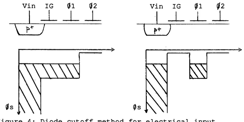
Vin IG
01
02
Vin IG01
02
uu
un
XSSS
Figure 4: Diode cutoff method for electrical
input.
An
input
voltage,Vin,
is
applied to theinput
diode,
andthe
input
gate,IG,
is
pulsed on to a large voltage. Thisforms
a transmission gate or switch such that the area underIG and
01
is
filled with charge to the same potential levelas the source, a level determined
by
theinput
diode asshown
in
the left potential diagram of the figure. Theinput
gateis
then turned off as shownin
the rightpotential diagram of the figure. The charge under the
input
gate
is
pushed backinto
the source and the signal chargeis
trapped under
01.
For a surface-channel CCD theinput
charge can
be
approximated as:Qsig
= AVs (Cox +Cd)
[image:34.558.70.469.111.311.2]where: AVs
is
the change of the surface potentialdue
to theinput
signal on the sourceCox
is
the channel oxide capacitance under gate2,
and
Cd
is
thedepletion
capacitance. The signal chargeis
non-linearly
related to theinput
voltage through thenon-linear
depletion-layer
capacitance of the silicon. If the output stage of the CCDhas
a depletion layercapacitance which
is
matched to that of theinput
node, goodoverall
linearity
can be obtained.However,
thereis
aninherent
non-linearity
in
the charge-to-voltage conversionwith this
input
technique.The
primary
advantages of this technique areits
simplicity and speed. This
input
method tends to beindependent
of the clock frequency. The primarydisadvantages
are that the excess charge stored under IGspills unpredictably
into
the receiving well when theinput
gate turns off,
giving
rise to excess noise and excess non-linearity. Also the signal chargeis
sensitive tovariations
in
the threshold voltage Vt under01
whichis
related to the flatband voltage Vfb.
Output Circuit
Three methods are available for the
detection
of chargesignals at the output:
1)
Current sensing3)
Nondestructive sensingCurrent
sensing
of the output of a CCD consists ofmeasuring
the current
flowing
in
the drain of aCCD,
as shownbelow.
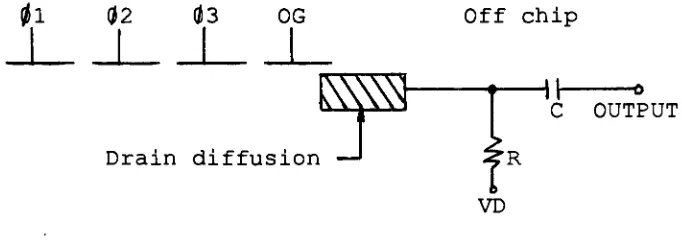
Il
02
03
OG Offchip
ion
I
1
II-C OUTPUT
Drain diffusa
Figure
5:
Currentsensing
techniqueVD
The current results from charge signals coupled to the
drain diffusion
by
the output gate electrode. The outputsignal takes the form of a current spike at a relatively
high capacitance terminal. The method provides a very
linear detection scheme.
[image:36.558.105.446.137.257.2]4.2
THREE-PHASE
CLOCK CIRCUITOne
way
ofrealizing
the clocked J-Kflip-flop
is
with two S-R
flip-flops
connectedin
a master-slavearrangement as shown
in
Figure 6.,
V
S"MASTER"
R
P
S"SLAVE"
R J
r
J
y
^lOCK ~*
y
v
y
Q,
h^_
Figure
6:
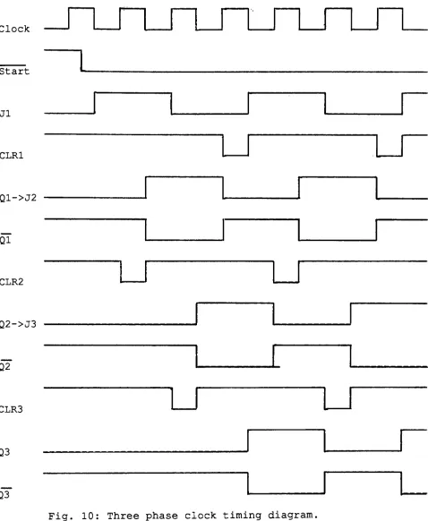
Master-Slave J-K flip-flop.The state change of the master takes place on the
leading
edge of the clock pulse, and the state change of the slave
follows on the
trailing
edge. The change of stateis
initiated
by
the clock pulse and neverby
a changein
J orK.
Any
changesin
the J and Kinputs
must occur betweenclock pulses.
The circuit,
implemented
using NOR gatesfor
pMOSClock.
Figure 7: NOR gate realization of Master-Slave J-K ff.
Changes
in
the J and Kinputs
occur when the clockis
"H"(-15v)
, and the datalatches
through when the clock goes to"L"
(15v)
. Since there are somany
transistorsin
thiscircuit, a circuit analysis program
SPICE,
version2G.5,
wasused to model the electrical behavior of these transistors.
The spice model parameters used are for the
intended
fabrication sequence, and have been extracted from
previously
fabricated
pMOSFETs. Alisting
of the analysisprogram, with the resulting voltages
corresponding
to thenodes
indicated
in
thefigure,
is
givenin
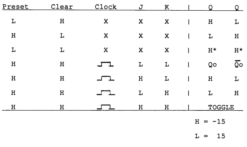
Appendix A.Additional
inputs
such as preset(PR)
and clear(CLR)
can
be
used to set theflip-flop
to statesindependent
ofthe clock. A "L"
applied to the clear
input
will reset theflip-flop
toQ="L",
and a "L" applied to the presetinput
will set the
flip-flop
to Q="H". Theseinputs
override theclock and J-K
inputs.
Thatis,
a "L" applied to the CLRinput
will reset theflip-flop
regardless of the values ofJ,
K and the clock. Under normal
operating
conditions, a "L"should not
be
simultaneously
applied to CLR and PR. When theCLR and PR
inputs
areboth
held
atlogic
"H"(or not
connected) the
J,
K,
and clockinputs
operatein
the normalmanner. The
following
table summarizes the next stateconditions.
Preset Clear Clock
L
H
L
H
H
H
H
H
L
L
H
H
H
H
X
X
X
J K
Q
Q
X X H L
X X L H
X X H* H*
L L Qo Qo
H L H L
L H L H
H H TOGGLE
H = -15
L =
15
Table
1:
Master-Slave J-K ff with PR and CLR.The figure on the
following
pageillustrates
the NORgate realization of the master-slave clocked J-K
flip-flop
with clear
(CLR)
and preset(PR)
inputs.
The CLRinput
is
used
in
constructing the overlapping3-phase
clockcircuitry
[image:39.558.57.462.253.494.2]^\
ClockFig
8: NOR gate implementation of J-K ff with PR and CLR.The preset and clear
inputs
can be accomplished withthe addition of six extra gates:
X14,
X15,
X16,
X17,
X18 andXI
9
to the J-Kflip-flop
already
presented. These gates areadded
into
the "slave"S-R
flip-flop
two between gates X5and X7 and two between gates X6 and X8. An
inverter
is
addedbetween the CLR and PR
inputs
before
going
into
gates X7 andX8,
respectively, so that theseinputs
willbe
active lowinputs.
Thisis
the complete circuit that constitutes theJ-K
flip-flop,
designed using NOR gates forfabrication
using the standard pMOS process.
This circuit
is
too complicated to simulate with theSPICE program. Because of the amount of
feedback
in
thecircuit, SPICE has a hard time reaching convergence. A
timing
diagram mustbe
generatedby
specifing
logic
valuesat the various
inputs
and outputs of the gatesto
analyzethis sequential network.
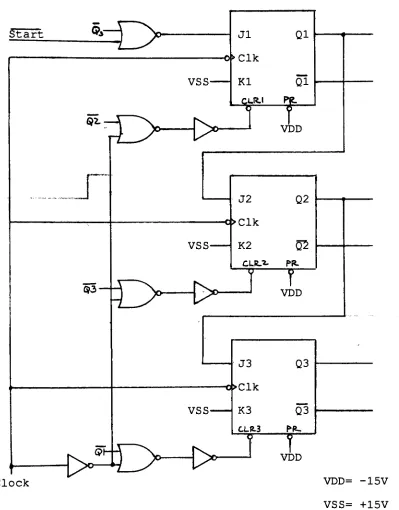
Three
of these J-K flip-flops canbe
puttogether,
along
with some additional circuitry to form anoverlapping
3-phase
clock.Start
Qs
Clock
Q-l
T
Q3-^
vss-Jl
OClk
Kl
Ql
Ql
S^L
{>
VDD
VSS-J2 Q2
OClk
K2 Q"2
CLKJi- PR. T7
{>
VDDT
vss-J3 Q3
>Clk
K3 Q3
CLR.3
PR--o
T
VDDVDD= -15V
VSS= +15V
[image:41.558.88.487.114.624.2]The
timing
diagram
for this circuitis
asfollows:
Clock
Start
Jl
CLR1
Q1->J2
Ql
CLR2
Q2->J3
Q2
CLR3
Q3
Q3
Fig. 10: Three phase clock
timing
diagram. [image:42.558.41.519.91.673.2]5.0
FABRICATION
5.1
PROCESSING
The
fabrication
sequence started with the growth of a2800
angstrommasking
oxide on6
N-type <100>3.5
ohm-cmwafers. Windows were opened
in
the oxide and boron wasdiffused
todefine
theinput
and outputdiodes,
the clockbusses
to the electrodes and the source anddrains
of thedigital
structures. The masking oxide was etched away andre-grown to
approximately
3100
angstroms, windows wereopened to define the gates. A 700 angstrom gate oxide was
grown
in
dry
02
on wafers1-3,
and a 1000 A gate oxide wasgrown on wafers 4-6. Contact windows were etched
in
the gateoxide. The wafer was coated with a thick layer of aluminum,
and the electrode structures were fabricated using the
shadow mask technique. This technique allows the device to
be fabricated using the pMOS process with added steps to
account for the extra metal
layer.
The process requiresfive masks;
diffusion,
thin oxide, contact cut,first
levelmetal (called POLY
in
this process), and secondlevel
metal.For a detailed summary of the process refer to Appendix C.
The single-level metalized gate CCD requires
extremely
close spacing between the electrodes so that their
depletion
regions overlap. The minimum electrode separation must
be
place. A minimum
feature
size restriction of 10 micronshas
been
established as a result of the use of silverhalide
masks at RIT. This dimension parameter
is
critical for theproper alignment of
device
geometries. This restriction wasovercome
by
using
a shadow-mask technique to achieve theelectrode separations.
The
first
level
of metal was deposited through theevaporation of 2 aluminum pellets for a 3000 angstrom film
in
a CVC evaporation system.Every
other electrodein
thearray
is
defined
with photoresist on this thick layer ofmetal. metal
is
then etched to clear, and thendeliberately
over-etched to form shadowed areas around thegates. .The
controllability
of this procedureis
goodproviding, the resist chosen
is
correctly
spun and baked toensure adhesion. There
is
somesolubility
of the resistitself
although theonly
effect of thisis
tomarginally
modify
the anticipated gap size. Resistdrooping
in
theoverhang
areasis
not a problem when aluminumis
chosen asthe gate metal. Another factor
in
the degree ofshadowing
choosen which must
be
consideredis
the lateral migration ofthe second level metal when
it
reaches the substrate. Foraluminum this
is
typically
3000
angstroms, andis
a functionof the evaporation conditions. Because of this lateral
migration
it
is
necessary to choose an underetchingdimension which
is
greater than the gap whichis
finally
required. The metallization procedure
is
completedby
thedeposition
of a second aluminiumfilm
over the entire wafer.The remaining
device
features aredefined
in
a subsequentphotoresist application
forming
theintermediate
gates,separated from metal
1
gatesby
a narrow shadowed gap. Thephotoresist
is
then removed,taking
the overlying film ofaluminum with
it;
thisis
commonly called a "float off"technique. Solvent access to the photoresist
is
guaranteedby
virtue of the overhang, and the unwanted metal over theresist
is
lifted offin
an ultrasonic acetone soak. Theresult
is
a linear array of electrodes, with the seperationsbetween them
determined
by
the degree of overetch.Using
this technique
it
is
possible to fabricate single levelmetal structures with spacings as close as one
half
of amicron. This lower
limit
is
imposed
to allow for thelateral surface migration of aluminum
during
the secondmetal
deposition,
which could short thedevice.
Figure 11shows this metallization sequence.
Photoresist
L Aluminium r
^^^^^t^^M?
(o)
Over-etch
Second
,deposition
Narrow gaps
'Shadowetch'
5.2
FABRICATION
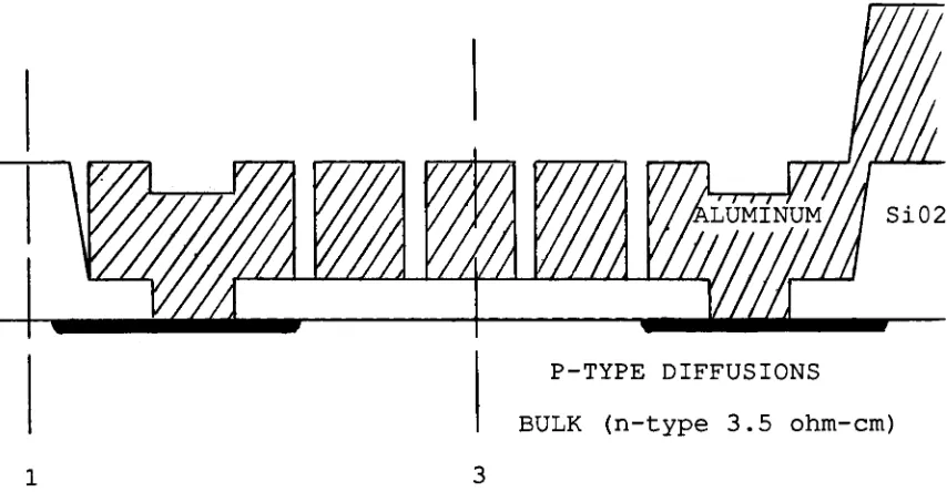
SIMULATIONA sequence of cross-sectional views of the CCD and a
pMOS transistor as the wafers go through the process
is
given
in
Appendix B. SUPREM (StanfordUniversity
ProcessEngineering
Models program) was used to analyze thefabrication
process.There are three specific regions of
interest,
where theoxide
thickness,
junction
depths anddoping
profiles shouldbe
calculated. In region one where the thick oxide occurs,information
about the diffusion of dopantsin
the Si02 canbe found. This
information
will reveal whether or not theoxide grown was thick enough to successfully
keep
thediffusion of
impurities
from reaching the silicon. Regionone also gives the thick oxide device threshold voltage. An
analysis of region two yields the projected final drain and
source diffusion
junction
depths as well as their sheetresistances. Region three provides
information
about thegate oxide thickness and the expected amount of phosphorous
pile up under the gate of the MOSFET at the Si-Si02
interface,
which allows simple projected threshold voltagecalculations. SUPREM's calculation
is
a very simple onewhich only involves the surface
doping
and surface statedensity,
so the value can only be considered as abest
casefigure. Complete SUPREM output listings
analyzing
theseregions are contained
in
Appendix D.Figure
12 on thefollowing
page shows a cross-sectionof a pMOS transistor and Figure
13
shows a cross-section ofthe CCD used to model the fabrication process. The next
three pages summarize each of the process steps and the
information
presented after each of these steps for thethree regions shown
in
eachfigure.
The predicted values given
by
SUPREM from thesesimulations are
listed
in
Table2,
following
the regionP-TYPE DIFFUSIONS
BULK (n-type
3.5
ohm-cm)1
2
3
Figure 12: pMOSFET cross sections for SUPREM simulation.
P-TYPE DIFFUSIONS
BULK (n-type
3.5
ohm-cm)1
3
Figure 13: CCD cross sections for SUPREM simulation.
(1)
Field oxide or cross-over region(2)
Drain or source diffusion region(3)
Gate region [image:48.558.58.500.77.295.2] [image:48.558.61.488.354.576.2]SUPREM-1
Field
oxide cross-sectional cut simulationStep
1: Do thediffusion
mask oxide growth.Leave the oxide on where the diffusions will
be
in
in
order to look at the oxide masking capabilityof the oxide.
Step
2
Step
3
Step
4Step
5
Step
6:Step
7Do the diffusion
into
the Silicon Dioxide.Do an oxide growth to
help
remove the boron skin.Etch off all the oxide grown.
Re-grow the thick field oxide over the area where
the diffusion was masked.
Field oxide re-growth thickness
Leave the regrown oxide to determine the change
in
the
field
oxide thicknessduring
the thin gateoxidation.
Do the gate oxide
in
dry
02.Set up the special purpose model to calculate the thick field oxide
device
threshold voltage.The gate material
is
aluminum, the bulk contactis
on thebackside,
and the surface statedensity
is
QSS=1.0ell.Field oxide thickness after gate oxidation
Thick oxide
device threshold
voltagebefore
sinter
Do a
drive
in,
in
a neutral ambient for the lengthof time that was used for the sinter, assume that the sinter reduces the value of the surface state
density
to QSS=1.0el0.Thick oxide
device
threshold voltage afterSUPREM-2
Diffusion
cross-sectional cut simulationStep
1: Do the diffusion mask oxide growth.Diffusion
mask oxide thicknessStep
2:
Etch the oxide where the diffusions willbe.
Step
3:
Do the diffusionsinto
the Silicon.Mid diffusion junction depth
Mid
diffusion
sheet resistanceStep
4: Do an oxide growth tohelp
remove theboron
skin.Oxide growth
during
diffusionPost diffusion
junction
depthPost diffusion sheet resistance
Step
5:
Etch the oxide grown at the end of the diffusion step.Step
6:
Re-grow the thick field oxide over thediffusion.
Leave the re-grown oxide to
find
the field oxidethickness after the thin gate oxidation.
Oxide re-growth over diffusion
Diffusion
junction
depth after re-growthDiffusion sheet resistance after re-growth
Step
7: Do the gate oxidein
dry
02.Diffusion junction depth after gate oxidation
Diffusion sheet resistance after gate
oxidation
Field oxide thickness over diffusion after
gate oxidation.
Step
8:
Do a drivein,
in
a neutral ambientfor
thelength
of time that was used for the sinter
Thick oxide device threshold voltage after
sinter
SUPREM-3 Gate oxide cross-sectional cut simulation
Step
1: Do the diffusion mask oxide growth.Leave the oxide on where the diffusions will be
in
in
order to look at the oxide maskingcapability
of the oxide.
Step
2:
Do the diffusioninto
the Silicon Dioxide.Step
3:
Do an oxide growth tohelp
remove the boron skin.Step
4: Etch off all the oxide grown.Step
5: Re-grow the thick field oxide over the area wherethe diffusion was masked.
Field oxide re-growth thickness
Step
6:
Etch the regrown oxide to define the thin gate oxide regions.Step
7: Do the gate oxidein
dry
02.Set up the special purpose model to calculate the
thick field oxide device threshold voltage.
The gate material
is
aluminum, the bulk contactis
on thebackside,
and the surface statedensity
is
QSS=1.0ell.Gate oxide thickness
Thin oxide device threshold voltage
before
sinter
Step
8:
Do a drivein,
in
a neutral ambient for the lengthof time that was used for the sinter, assume that
the sinter reduces the value of the surface state
density
to QSS=1.0el0.Thin oxide device threshold voltage after
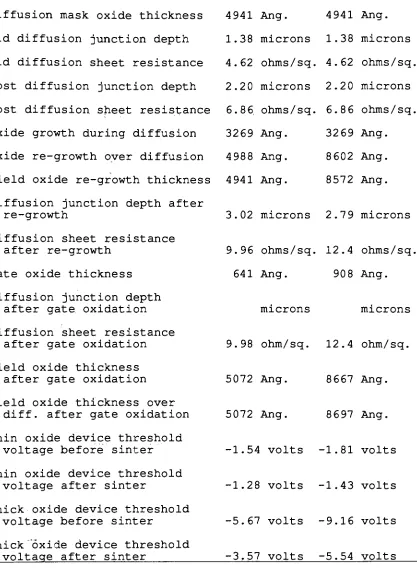
Quantity
Transistor CCDDiffusion mask oxide thickness
Mid
diffusion
junction
depthMid
diffusion
sheet resistancePost
diffusion
junction
depthPost
diffusion,
sheet resistanceOxide growth
during
diffusionOxide re-growth oyer diffusion
Field oxide re-growth thickness
Diffusion
junction
depth afterre-growth
Diffusion sheet resistance
after re-growth
Gate oxide thickness
Diffusion
junction
depthafter gate oxidation
Diffusion sheet resistance after gate oxidation
Field oxide thickness
after gate oxidation
Field oxide thickness over
diff. after gate oxidation
Thin oxide
device
thresholdvoltage before sinter
Thin oxide device threshold
voltage after sinter
Thick oxide device threshold
voltage
before
sinterThick oxide
device
thresholdvoltage after sinter
4941 Ang.
1.38
microns4.62 ohms/sq.
2.20
microns6.8
6
ohms/sq.3269
Ang.498 8 Ang.
4941 Ang.
4941 Ang.
1.38 microns
4.62 ohms/sq.
2.20
microns6.8 6
ohms/sq.3269 Ang.
8602 Ang.
8572 Ang.
3.02
microns2.79
microns9.96
ohms/sq. 12.4 ohms/sq.641 Ang. 908 Ang.
microns microns
9.98 ohm/sq. 12.4 ohm/sq.
5072 Ang.
5072 Ang.
8667 Ang.
8697 Ang,
-1.54 volts -1.81 volts
-1.28 volts -1.43 volts
-5.67 volts -9.16 volts
-3.57 volts -5.54 volts
Table
2:
SUPREM PREDICTIONS FOR TRANSISTOR AND CCD SHOWN IN FIGURES 12 AND 13. [image:52.558.76.493.56.625.2]5.3
LAYOUTThe
digital
pMOS structures needed to construct the J-Kflip flop
are a threeinput
NOR gate, a twoinput
NOR gateand an
inverter,
. The geometries and alignmentfor
thediffusion,
oxide, metal and contact cut layers placedin
?
~"l
1
1
i
'1
1
?
1
i
1
?
['
1
[image:53.558.44.519.125.632.2]proper position together to form these three structures
is
shown
in
Figure 14. The length of the upper gatesin
allthree structures
is
Lu =60Um,
the width of the upper gatesis
Wu = lOUm. The lower gate lengths are L = lOUm. Thelower width of the NOR gate structures
is
W =lOUm,
andfor the
inverter
W = 30Um.Making
the structures all thesame height facilitates connecting the Vdd and Vss buss
lines. The arrangement of these elements along with the
proper interconnections of the gates to form the J-K
flip-flop
is
shown in Figure 15.>5T
CL&-Figure 15: J-K
flip flop
layout.A program called
ICE,
Integrated CircuitEditor,
wasused to create this artwork to generate the masks for each
of the four layers. A
listing
of the process file usedin
the design which defines the paramaters required
by
ICE todevelop
the layoutis
included at the end of this section. [image:54.558.62.500.50.498.2]Illustrated
in
thefollowing
figure
is
the CCDlayout
03
,-,
3
P
3
P-
i iD ?
-
P
>kHfc
?! D n d n D D
w
m
D D D DD
D ?
Ob
<2>2-Figure 16: CCD Layout.
The yellow
patterning
represents the extra metal masklayer,
called POLY
in
this process, used todefine
every otherelectrode. This
is
the metal layer that getsslightly
overetchedbefore
the second layer of metalis
applied.With the addition of a few extra gates and the proper
interconnections,
the three J-Kflip-flops
form theoverlapping
three phase clock circuit tosequentially
pulse [image:55.558.54.501.97.391.2]circuit connected out to 12 pads for probing. A J-K
flip
flop
is
located
in
the upperleft
hand
corner, and a CCDarray
in
the lowerleft
corner.Figure 17:
Chip
Layout [image:56.558.50.510.145.564.2]TEST_CHIP
chip
width = 4000chip height = 4000 10 layers
layer metal 0 anti regions
plot 1 graphics 1
layer oxide 1 anti regions
0 0 150-800
plot 2 graphics 2
layer graphics 0 anti regions plot 3 graphics 3
layer diff 1 anti regions 0 0 150 BOO
plot 4 graphics 4
layer extra 0 anti regions plot 5 graphics 5
layer emitter 1 anti regions 0 0 150 800
plot 6 graphics 6
layer cc 1 anti regions
0 0 150 800
plot 7 graphics 7
layer
poly
1 anti regions 0 0 150 800plot 8 graphics 8
layer Implant 1 anti regions
0 0 150 800
plot 9 graphics 9
layer metal2 1 anti regions
0 0 150 800
plot 10 graphics 10
angle 0 space angle 0 space
angle 0 space
angle 0 space angle 0 space angle 0 space
angle 0 space
angle 0 space
angle 0 space
angle 0 space angle 0 space
angle 0 space angle 0 space angle 0 space angle 0 space
1 color 1 pen 3 fill 0
2 color 2 pen 2 fill 0
3 color 3 pen 4 fill 0
4 color 4 pen 4 fill 0 5 color 5 pen 5 fill 0
6 color 6 pen 6 fill 0
7 color 7 pen 1 fill 0
8 color 8 pen 7 fill 0 9 color 1 pen 5 fill 0
10 color 2 pen 3 fill 0
11 color 3 pen 3 fill 0
12 color 4 pen 4 fill 0
13 color 5 pen 5 fill 0
6.0
RESULTS6.1
FABRICATIONThe actual fabrication parameters can
be
compared withthe SUPREM predictions. The results are
listed
in
Tables3
and 4 at the end of this section. Table
3
compares thepredictions
for
the
CCD,
whichhad
a targeted gate oxidegrowth of
1000
A. Table 4 compares the predictions for thedigital structures, which
had
a targeted gate oxide growthof
700
A. The run was splitbecause
a700
A gate oxideis
optimum for transistor structures,
but
the thicker1000
Agate oxide gives a smaller ratio of
gap
width to oxidethickness for
better
charge transfer performance of the CCD.Measurement of the parameters from the wafers compared
reasonably well with the predictions, with the exception of
the diffusion parameters. The diffusion sheet resistance on
the thick gate oxide wafers
is
to high to yieldworking
devices.
Testing
also showed that the1000
A gate oxidegrowth caused the,, diffusions to spread to
far,
increasing
the sheet resistance, and the transistors acted as resistors
and never turned on. The thick and thin oxide
device
threshold voltage measurements were not made
before
andafter sintering.
'The
after sinter values couldnormally be
obtained from the test chips
included
on the wafer,however,
the
metal mask ofthe
testchip
did
not alignto
the otherlayers.
The
results obtainedfrom
fabrication can serve asa
baseline
for
future
processes.The
nexttwo
figures
are photographs of one of the CCD!'
iqurr 1 8 : Kabi i cat od CCD
[image:59.558.100.455.111.646.2]structures and one of the J-K
flip
flops
fabricated.The
electrodegap
length
andinter-electrode
spacing
ona typical
device
is
illustrated
in
the photo below. A 1336Xmagnification gives a conversion ratio of .7486
Um/mm,
measurements off the photo show an electrode width of 1.9in
and a
gap
length
of0.1 2 in.
Converting
to Um gives a:^iSfe"*1
x "Ul,r^x
^^
=36.6
Umgate width
nJM&Xtas
x .CL&Uix
2SSd^
=2.3
Umelectrode
iv\rt\ in gap
Figure
20:
CCD electrodes [image:60.558.59.501.199.607.2]These
dimensions
were typical across the wafers,showing
good
repeatability
of the shadow mask technique.Shown below are some of the
digital
pMOS structures.An E-beam
has
been
applied to thediffusion
regions, shownin
the upperleft
photograph,
causing
electrons tobe
sweptacross
the
electricfields
of the metallurgicaljunctions,
"highlighting"
the
diffused
regions.Figure
21:
pMOS structures anddiffusions.
,: [image:61.558.39.520.187.622.2]The
next photograph shows where the wafer was cleaved,across a source
diffusion.
By
applying an electronbeam,
the metallurgical
junction
depth
into
the waferis
shown.This
depth
canbe
measured off the photograph,taking
into
account that the tilt of the wafer with respect to the beam
is
45,
The
junction
depth
is
approximately
3.5
Um.Figure
22:
Cut through diffusion and pnjunction,
[image:62.558.34.518.68.665.2]The next two SEM*s were taken on the CCD. A
diffusion
opening
to an electrodeis
shown. A closeup
of a metalline
making
the transition from the thick oxide to the gateelectrode
is
shownin
the square and the closeup
insert.
[image:63.558.44.517.65.644.2]The
following
![Figure 2: Energy band and blockcharge diagrams.[14 ]](https://thumb-us.123doks.com/thumbv2/123dok_us/110515.10340/23.558.119.461.86.630/figure-energy-band-and-blockcharge-diagrams.webp)
![Figure3:ACcharge fluctuations inanMOS capacitor.114]](https://thumb-us.123doks.com/thumbv2/123dok_us/110515.10340/24.558.71.488.182.615/figure-accharge-fluctuations-inanmos-capacitor.webp)