International Journal of Innovative Technology and Exploring Engineering (IJITEE) ISSN: 2278-3075, Volume-9 Issue-2, December 2019
Abstract: This paper concentrates on the design of DC multiplier for solar photovoltaic application. The main aim of this paper is to boost up the voltage from solar panel without using transformer and to track maximum power using maximum power point algorithm. The system design includes solar panel, snubber circuit, switching circuit, coupled inductor, opto isolator, voltage multiplier, microcontroller and load. Normally boost converter is used in conjunction with solar PV to boost the output voltage from panel. But the boost converter can be able to increase the input voltage to a limited value. In other, converter transformers are used. Hence core loss, magnetic loss and copper loss will occur. To overcome these losses and also to achieve isolation coupled inductor can be used. Thus proposed system overcomes the core loss, magnetic loss, copper loss and also helps to achieve the isolation between the circuits by using the coupled inductor. By using voltage multiplier, the boost converter can able to increase the input voltage beyond the rated value. Simulations are done in MATLAB/Simulink platform. It forms the voltage multiplier for renewable energy application to boost the DC voltage.
Index Terms: Photovoltaic system, Boost Converter, MPPT Algorithm, Snubber Circuit, Coupled inductor, Microcontroller and Voltage multiplier.
I. INTRODUCTION
The demand for electricity will keep on expanding as long as total population increases and people keep on requesting a higher standard of living. The challenge lies in giving this electricity from dependable and reasonable sources while keeping up regard for the surrounding. Thermal power and other fossil fuel based energy sources are currently available resource in production of electricity. But additionally it also causes some unfortunate consequences on the surrounding. While it is clear that renewable energy is an alternate energy source in production of electricity.
Renewable energy as of now faces a few disadvantages on its track to become the sole source to generate electric power. Solar energy is mainly depend on the geographic location and it is one of the major drawback of it. For instance, the best areas to reap solar energy lie in the desert locales of earth's surface. The photovoltaic solar energy is used to convert the irradiation into electrical energy and supplies all electrical loads. There are different topologies
Revised Manuscript Received on December 05, 2019.
A.Jeyashree, Assistant Professor, PSG Institute of Technology and Applied Research, Coimbatore, Tamil Nadu, India
P.Sathish Kumar, Assistant Professor, Sri Shanmugha College of Engineering and Technology, Sankari, Salem Tamil Nadu, India
A.Imtiyas, Assistant Professor, Vivekananda College of Engineering for Women, Namakkal, Tamil Nadu, India
and design for embedding converters are introduced to improve the efficiency of the existing system[1-4]. However,
the majority of the energy consumers don't dwell in these parched locales. The alternate of solar energy is wind energy, but it’s also depending on the geographic location. The voltage regulation is also vital parameter to transfer energy for wearable electronics application using inductor sizing [5-6].
The main objective of this paper is to boost up the voltage from solar panel without using transformer and to track maximum power using maximum power point algorithm. The exciting system consists of isolation transformer and voltage doubler. The efficiency of the conventional system is 94% only. But in proposed system the efficiency is 98% because of using voltage multiplier and coupled inductor. Here MPPT algorithm (P & O algorithm) is used to track maximum power from solar panel at different irradiation [7-8]. An isolated coupled inductor coordinated DC-DC converter with a snubber circuit to lessen the voltage spike on switches. The low turn's proportion is accomplished by diminishing the extent of the coupled inductor, accordingly improving effectiveness.
II. PROPOSEDTOPOLOGY
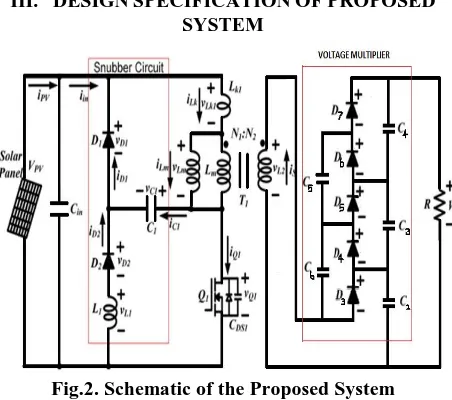
Figure 1 represents the layout of the proposed topology. It comprises of a dc source, boost converter and load. Here the solar panel acts as an input DC supply. The output of the solar panel is fed to the boost converter. The boost converter consists of snubber circuit at primary side and voltage multiplier at secondary side. The dc-dc converter boosts up the voltage. The boosted dc voltage is given to the resistive load. The pulses are generated using microcontroller. The input of the microcontroller is 5V (2-5). Opto-isolator is to give detachment between low dimension gate circuit and the abnormal state power circuit.
Design of A Novel DC Multiplier for Solar PV
Energy Applications
Fig.1. Block Diagram of Proposed System III. DESIGNSPECIFICATIONOFPROPOSED
[image:2.595.57.283.270.470.2]SYSTEM
Fig.2. Schematic of the Proposed System
For the proposed system, the design procedure for voltage multiplier with respect to solar PV application is shown below
i).Solar Panel Specification:
Table No.1. Specification of Solar PV Panel
S.No Parameter Values
1. Maximum Power 200 Watts
2. Open Circuit Voltage, Voc 34.1 Volts
3. Short Circuit Current, Isc 8.81 Amps 4. Voltage at Maximum
Power Point, Vmp
30.2 Volts 5. Current at Maximum Power
Point, Imp
8.06 Amps
6. No. of Parallel String 10
7. Series Connected Module Per String
1
The design procedure and the values are calculated using the operation of the proposed circuit for voltage multiplier circuits.
ii). Duty Cycle:
iii).Turns Ratio:
iv). Design of Coupled Inductor:
v).Snubber Capacitor:
vi). Snubber Inductor L1:
International Journal of Innovative Technology and Exploring Engineering (IJITEE) ISSN: 2278-3075, Volume-9 Issue-2, December 2019
Voltage Multiplier:
The input voltage from the transformer is boosted according our simulation requirement. The explanation for the voltage multiplier circuit is analyzed below. The basic voltage multiplier circuit is shown with necessary equations.
The output voltage across VC1 and VC2. Assume, the capacitor C1 and C2 are discharged initially. For positive half cycle, the figure is shown below
Then the voltage across the capacitor is By applying KVL, VC1= +Vm
For negative half cycle, the figure is shown below
Then the voltage across the capacitor is By applying KVL, VC2 = +Vm
BY applying KVL to entire loop shows, Vout = VC1+VC2 = 2Vm
In this model, the voltage is doubled and thus the output voltage is boosted according to the capacitor location and the diode arrangement and act as a voltage multiplier. Thus, the coupled inductor and capacitor plays a vital role in boosting the voltage to the higher value for solar photovoltaic application [9]. This type of inductor sizing is also employed for AC applications [10].
IV. SIMULATIONRESULTS
The voltage multiplier is simulated and connected to output of the panel is connected to the coupled inductor. The
simulation results are obtained by using MATLAB/Simulink platform.
Fig.3. Simulation of Proposed System
Fig.5. Gate Pulse from MPPT
Fig.6. Output Voltage
Fig.7. Load Current
Table No. 2. Simulation Results Parameter Values in
Conventional Converter
Values in Proposed Converter
Solar Voltage Vpv
24 V 24 V
Operating Frequency
50 kHz 50kHz
Output Voltage Vo
200 V 260 V
(Voltage Doubler is used)
( Voltage Multiplier is
used) Maximum
Input Power
200 W 200 W
Efficiency 96% 98%
V. CONCULSION
Thus the photovoltaic system output is enhanced using the power conversion topologies. The voltage of the solar panel is boosted up without using the transformer and the maximum power point is tracked using the MPPT algorithm. The simulation results show that the usage of voltage multiplier with boost converter lead to boost up the input voltage beyond the rated value with increased efficiency. Due to the absence of transformer the losses are avoided and the isolation between the circuits is achieved by using the couple inductor. It has been demonstrated that the proposed control conspire perform sensibly well and the goal of voltage boosting is achieved.
REFERENCES
1. Christopher D. Lute. “An Improved Dc-Dc Converter for Photovoltaic
Power System Applications” The Board of Trustees of the Colorado School of Mines.
2. P. Denholm, et al., “Bright future: solar power as a major contributor to
the U.S. grid,” IEEE Power & Energy Magazine, vol. 11, no. 2, pp. 23-32, Mar. /Apr. 2013.
3. M.G. Villalva, et al., “Comprehensive Approach to Modeling and
Simulation of Photovoltaic Arrays,” IEEE Trans. Power Electron., vol. 24, no. 5, pp. 1198-1208, May 2009.
4. A.Imtiyas, P.Sathish Kumar, U.Shyamala Devi. “Induction motor driven
water pump fed by solar photovoltaic array using boost converter” International journal of mechanical engineering and technology (IJMET) 2018, pp: 336-347.
5. Mofan Tian, Xu Yang, Yang Chen, Laili Wang. “A Cable Type
Packaging for Voltage Regulation and Energy Transport in Wearable Energy Harvesting Systems”. IEEE Transaction on Power Electronics. Vol-34 Aug 2019, 7116-7120.
6. Shih-Kuen Changchien, J.F. Chen, Tsorng-Juu Liang, Lung-Sheng
Yang. “Novel High Step-Up Dc-DC Converter for Fuel Energy
Conversion System” IEEE Transactions on Industrial
Electronics 57(6):2007 - 2017 · July 2010.
7. N. Mhiri, K. Ammous, A. Alahdal, H. Ghulman, and A. Ammous,
[image:4.595.62.272.62.422.2] [image:4.595.61.271.462.728.2]International Journal of Innovative Technology and Exploring Engineering (IJITEE) ISSN: 2278-3075, Volume-9 Issue-2, December 2019
8. Nesrine Mhiri, Abdulrahman Alahdal, Hamza Ghulman, AnisAmmous
“A Novel Analog Circuit Design for Maximum Power Point Tracking of Photovoltaic Panels” Advance in Power Electronics, Sep 2017.
9. Yong-Seng Wong 1,2, Jiann-Fuh Chen 1,*, Kuo-Bin Liu 2 and Yi-Ping
Hsieh. “A Novel High Step-Up DC-DC Converter with Coupled Inductor and Switched Clamp Capacitor Techniques for Photovoltaic Systems”. MDPI March 2017.
10. Shih-Ming Chen, Tsorng-Juu Liang, Lung-Sheng Yang, J.F. Chen. “ A
Boost Converter with Capacitor Multiplier and Coupled Inductor for AC
Module Application” IEEE Transactions on Industrial
Electronics 60(4):1503-1511 · April 2013.
AUTHORSPROFILE
Jeyashree A currently working as a Assistant Professor in the Department of Electrical and Electronics Engineering at PSG Institute of
Technology and Applied Research,
Coimbatore. She completed BE (2011-2015) in the Department of Electrical and
Electronics Engineering and ME
(2015-2017) in the area of Power Electronics and Drives. She have supervised B.E (EEE) Projects for students working in the field of Power Electronics and Drives, Photovoltaic Energy and System Modeling using MATLAB. She was acting as a Life Member of ISTE and IAENG.
.
Sathish Kumar P currently working as a Assistant Professor in the Department of Electrical and Electronics Engineering at Sri Shanmugha College of Engineering and Technology, Salem. He completed B.E (2006-2010) in the Department of Electrical and Electronics Engineering and M.E (2010-2012) in the area of Power electronics and Drives. He supervised B.E (ECE) Projects for students working in the field of control system.