White Rose Research Online URL for this paper: http://eprints.whiterose.ac.uk/81644/
Version: Accepted Version
Article:
Mironov, BE, Freeman, HM, Brown, AP et al. (6 more authors) (2015) Electron irradiation of nuclear graphite studied by transmission electron microscopy and electron energy loss spectroscopy. Carbon, 83. 106 - 117. ISSN 0008-6223
https://doi.org/10.1016/j.carbon.2014.11.019
eprints@whiterose.ac.uk https://eprints.whiterose.ac.uk/
Reuse
Unless indicated otherwise, fulltext items are protected by copyright with all rights reserved. The copyright exception in section 29 of the Copyright, Designs and Patents Act 1988 allows the making of a single copy solely for the purpose of non-commercial research or private study within the limits of fair dealing. The publisher or other rights-holder may allow further reproduction and re-use of this version - refer to the White Rose Research Online record for this item. Where records identify the publisher as the copyright holder, users can verify any specific terms of use on the publisher’s website.
Takedown
If you consider content in White Rose Research Online to be in breach of UK law, please notify us by
Electron irradiation of nuclear graphite studied by transmission
electron microscopy and electron energy loss spectroscopy
B. E. Mironov1,*, H. M. Freeman1,*, A. P. Brown1, F. S. Hage2, A. J. Scott1, A. V. K. Westwood1, J. -P. Da
Costa3, P. Weisbecker4, R. M. D. Brydson1,2,
1
Institute for Materials Research, Univ. Leeds, Leeds, UK, LS2 9JT
2 SuperSTEM, STFC Daresbury Laboratories, Daresbury, UK, WA4 4AD
3
Univ. Bordeaux, BSA, Laboratoire de l’Intégration du Matériau au Systéme, UMR 5218 CNRS-IPB – Université de Bordeaux,33405 Talence, France
4
CNRS, Laboratoire des Composites Thermo Structuraux, UMR 5801 CNRS- Herakles- CEA - Université de
Bordeaux, 33600 Pessac, France
Abstract
Structural and chemical bonding changes in nuclear graphite have been investigated
during in-situ electron irradiation in a transmission electron microscope (TEM); electron
beam irradiation has been employed as a surrogate for neutron irradiation of nuclear grade
graphite in nuclear reactors. This paper aims to set out a methodology for analysing the
microstructure of electron-irradiated graphite which can then be extended to the analysis of
neutron-irradiated graphites. The damage produced by exposure to 200 keV electrons was
examined up to a total dose of approximately 0.5 dpa (equivalent to an electron fluence of 5.6
x 1021 electrons cm-2). During electron exposure, high resolution TEM images and electron
energy loss spectra (EELS) were acquired periodically in order to record changes in structural
(dis)order and chemical bonding, by quantitatively analysing the variation in phase contrast
images and EEL spectra.
1 Introduction
τver 80% of the UK’s current nuclear reactors are graphite-moderated Advanced Gas Cooled Reactors (AGR) or Magnox reactors [1]. In addition to moderating the energies of
neutrons in the fission process, the graphite core provides structural support, contains the fuel
and control rods and allows for coolant flow. The graphite blocks are subject to high levels of
neutron irradiation resulting in chemical and physical property changes, which in turn affect
neighbouring reactor components. The lifetime of such reactors is therefore primarily limited
*
by the performance of the irreplaceable graphite within the working reactor, so an accurate
measure of its condition is essential for economic success and plant safety.
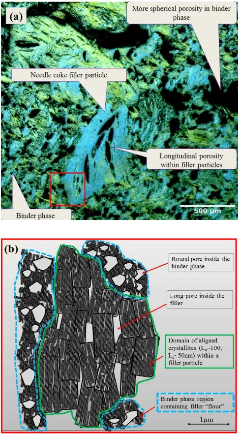
Figure 1 (a) Polarised light micrograph of pile grade A (PGA) nuclear graphite showing the main constitutive elements, with the outlined area in red corresponding to (b), a schematic of short range features within the filler particle (outlined in green) and binder phase (h outlined
in blue).
Nuclear graphite is a synthetic material produced from pitch and petroleum coke particles,
with a high degree of crystallinity following thermal treatment at high temperatures
(graphitization) [2]. When the graphitization process is complete, two main features can be
distinguished: the majority filler particles and a minority binder phase, both of which are
formed by domains of aligned individual crystallites and appear as a single colour in a
[image:3.595.71.315.112.553.2]ranging from Mrozowski cracks between crystallites (50 nm -10 m) to micro- and macro-
pores around domains and particles (Figure 1) [3].
For over 70 years, a considerable body of evidence has been assembled to understand the
behaviour of irradiated graphite [2,4–6]. The bulk properties of damage features have been
thoroughly investigated and theoretical models of induced structural changes derived [7].
Although this has allowed property changes in the irradiated bulk to be partly understood and
accounted for in current and future graphite based reactor designs, the mechanisms of such
processes at the nanoscale still remain uncertain. This work investigates the effect of electron
irradiation on nuclear grade graphites within a transmission electron microscope (TEM) in an
attempt to understand the fundamental processes involved in radiation damage.
Early work, by Mitchel et al. (1965), investigated the effects of electron irradiation
through stored energy release following irradiation at high temperature [8]. In 1972 the
effects of electron irradiation to graphite were examined by Ohr et al. for the first time, who
reported a displacement threshold accelerating voltage of below 120 kV [9].
1.1 Irradiation of nuclear graphite
Throughout this paper we will compare the effects of neutron and electron irradiation
therefore it is important to understand the key differences between the two. The atomic
displacement rate of the carbon atoms in the graphite is measured in displacements per atom
(dpa) and is dependent on the kinetic energy of the incident particle [2]. According to
calculations by Thrower and Mayer [10] a 1 MeV electron and neutron produce an average of
1.6 and 500 atomic displacements respectively. It is generally understood that cascades of
atomic displacements are the most common route for large scale structural disturbances and
models have been developed to calculate the number of atoms involved in cascade events
resulting from different incident energies [11].
When mimicking the effects of neutron irradiation damage with electron irradiation in the
TEM, it is important to account for both the higher dose rate of electrons compared to
neutrons in a nuclear reactor (greater by about 104) and the reduced displacements per atom
from electrons due to the lower mass [12]. Electron irradiation causes point defect damage
whereas the higher mass and lower dose rate of neutrons causes cascade damage. However, the relatively wide spacing of graphite’s basal planes results in a low density of the cascade events, and the low neutron dose rates (10-7 dpa s-1) and high temperatures (~450 °C) in the
nuclear reactor allow damage to partially anneal out between cascade events [13–15].
coalesce into clusters and gradually deform the crystal lattice ultimately resulting in both
chemical and physical changes. Damage accumulation at temperatures below 200 °C
increases the Wigner energy of the graphite, due to a lack of atomic diffusion [16]. It is
widely agreed that single vacancies become mobile at 100 – 200 °C whereas interstitial atoms
become mobile at temperatures of 500 °C [17]. Thus only at higher temperatures such as
those in the Gen IV graphite moderated Very High Temperature Gas Reactors (> 300 °C)
does stored energy dissipation occur by diffusion driven atomic re-ordering and the problem
is addressed in the short term. Longer term exposure to a high temperature environment (>
400 °C) however, gives rise to creep and dimensional change [18–20].
The key observed changes in nuclear grade graphite as a result of neutron irradiation are
micro-crack closure resulting from expansion in the c-direction and dimensional change from
irradiation induced creep, both of which depend on the overall level of initial crystallinity
[16,21]. Dimensional change is determined in a number of ways, such as directly measuring
specimens before and after irradiation, using X-ray diffraction to assess crystallite behaviour,
and measuring changes in cracks and porosity with electron and light microscopy and
small-angle neutron scattering [18,19,22]. The fundamental dimensional changes are known to
involve crystallographic expansion in the c-direction and contraction in the a-direction [3].
Initially, the expansion is largely accommodated for in cracks and pores created during the
manufacturing process; Mrozowski cracks arise from the anisotropy in graphite thermal
expansion coefficients and lie perpendicular to the c-direction hence the initial
accommodation of expansion, so that the initial macroscopic response is a net shrinkage in
the a-direction [23]. Upon further irradiation and once the cracks and pores are fully closed,
irreversible net macroscopic expansion occurs. The transition between contraction and expansion is referred to as ‘turnaround’ [24,25].
Transmission electron microscopy is an established tool for characterising both electron
and neutron irradiated graphite [15,26]. There are however, very few detailed TEM-EELS
studies on nuclear graphites but a significant volume of work on graphitizing and
non-graphitizing carbons [27,28]. In this work we will focus on quantitative analysis of atomic
lattice imaging and EEL spectroscopy to elucidate the nanoscale changes that occur in
2 Experimental Details
2.1 Sample preparation
Virgin Pile Grade A (PGA) graphite sourced from the University of Manchester was
chosen for inspection. PGA is a medium to coarse grain anisotropic nuclear graphite of
typical density 1.74 g cm-3. The anisotropy of this particular graphite comes from the
tendency of the needle-like grain particles in the filler to align in the extrusion direction
during the manufacturing process. Samples were crushed using an agate pestle and mortar
and mixed with acetone before being dispersed onto a holey carbon-coated copper TEM grid
(3mm diameter; Agar Scientific Ltd). The analysed areas had a thickness less than 0.3 times the mean free path for inelastic scattering ( ).
2.2 Microscope conditions
TEM investigations were performed on an FEI CM200 field emission TEM operated at
197 kV with a tip extraction bias of 3.21 kV routinely providing an electron flux of
approximately 4.24 x 10¹⁸ electrons cm-2 s-1 and an EELS energy resolution of 0.7–0.8 eV,
measured as the full width at half-maximum (FWHM) of the ZLP. For EELS, the microscope
was operated in diffraction mode with the smallest selected area aperture inserted, giving a
circular projection of approximate diameter 150 nm, a collection semi-angle of 1.6 mrad and
a convergence semi-angle of approximately 0.8 mrad, (corresponding to the magic or
orientation independent angle [29]). Digital images and energy loss spectra were captured
using a Gatan Imaging Filter (GIF) 200 with a 1 megapixel slow scan CCD array. Data from
the array (i.e. images and spectra) were processed using Gatan’s Digital Micrograph
software.
Unless stated otherwise, all experiments were performed at room temperature where the
localised heating effect from the electron beam was considered to be negligible due to the
high thermal conductivity of graphite [30]. In-situ electron irradiation damage at higher
temperatures was investigated using a Gatan TEM heating holder.
2.3 Determination of dose
Throughout this paper we will refer to electron and neutron irradiation in three ways:
fluence refers to the number of electrons or neutrons that intersect a unit area; flux is the
fluence rate; and dose is the energy transferred at a given fluence. The dose, D (in dpa), is
calculated using Equation 2.1 where J is the electron fluence and d is the displacement cross
d J
D
Equation 2.1The displacement cross section varies with electron energy and displacement threshold
energy. Referring to figure 18 from Oen (1965) [31] we measure a displacement cross section
value of 16.25 barns for an electron energy of 200 keV and a displacement threshold energy
of 20 eV [32]. The value of displacement threshold energy has not yet been agreed upon
within the literature, with values ranging from 15 – 30 eV, resulting in a significant variation
in d and the resultant dose estimates [14,21,26,32].
During EELS experiments, the intensity of the beam was varied considerably for the
acquisition of low loss and core loss spectra resulting in an inconsistent electron flux. For the
acquisition of low loss spectra the beam was spread over a large area to give a low intensity
(so as to avoid saturating the ccd) resulting in a near-negligible flux; when collecting the core
loss however, the beam was focused over a smaller area giving a much higher intensity,
comparable to the intensity during imaging. The change in fluence was accounted for by
measuring the electron flux at the two acquisition intensities and recording the time spent at
each; the cumulative fluence was then determined and converted to dpa.
3 Results and Discussion
3.1 TEM
Four areas of thin (<50 nm) PGA graphite were subjected to an average electron fluence of
4.2 x 10¹⁸ electrons cm-2 s-1 (2.4 x10⁻⁴ dpa s-1). Images of the basal planes and electron energy
loss spectra were recorded periodically throughout. The micrographs and their corresponding
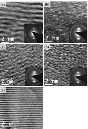
selected area electron diffraction (SAED) patterns shown in Figure 2 are typical of the
damage produced by a 200 kV electron beam. In particular, the tortuosity (or curvature) of
the (002) planes can be seen to increase, the spacing increases, and the lattice fringe length
decreases. These results suggest the breakup of the graphitic structure into nanocrystalline
regions with increasing dose, which in the high dose limit produce an amorphized structure.
These micrographs are comparable to those obtained by Karthik and Kane [21] and Muto
[33] who also investigated the effects of electron irradiation in nuclear graphite.
For comparison, Figure 2 (e) shows the effect of performing the same procedure at 400 °C.
Interestingly, significantly less alteration of the atomic structure is observed, suggesting that
damage is continuously annealed out at these temperatures. Further work is in progress to
provide qualitative analysis, understanding the exact mechanisms of defect creation remains
an area for investigation. A contrast change in a phase contrast TEM micrograph may not
necessarily relate to a change in atomic position but may instead be due to a change in
thickness or defocus. While every effort was made to ensure that images were acquired at
Scherzer defocus, awareness of the issues associated with contrast reversal is highly
important when analysing these disordered structures [34].
Diffraction patterns were also recorded at regular intervals during electron beam exposure
and the spacing of (002) spots were measured using intensity profiles in Digital Micrograph.
Figure 3 shows an increase in interplanar spacing of 10% following electron irradiation of
0.31 dpa, as measured from the diffraction patterns. The arcing of the diffraction spots was
also measured to assess the misalignment of layers induced during electron irradiation. To
extract this information the SAED patterns were intensity normalised and the full width at
half maximum (FWHM) of each diffraction arc was measured using a Graphite Anisotropy
Analysis Program (GAAP) provided by A. A. Campbell at the University of Michigan [35].
GAAP measures the intensity around a ring at the (002) radius the Gaussian curves are fitted
to the intensity plots and the FWHM determined. The data are presented in Figure 4 and
show a 40° increase in arcing of (002) diffraction spots following 0.86 dpa of electron
Figure 3 Change in interplanar spacing with respect to electron dose as measured from the spacing of (002) spot spacing in a series of SAED patterns. Error bars represent analytical error following the analysis of three damage series. Dose error = ± 6.4%
[image:10.595.80.513.429.670.2]TEM micrographs were also analysed, using software provided by the ‘PyroMaσ’ research group, to quantify the change in atomic arrangement following electron irradiation
[36]. Based on analysis of (002) lattice fringes, the software provides information on fringe
length, tortuosity and orientation using Fourier transform filtering and a level curve tracking
algorithm [37]. Although the algorithm detects fringes even if they exceed the image
boundaries, they cannot be accounted for when performing measurements since the true
length and tortuosity cannot be determined. Application of the software to ordered and
(electron irradiation induced) disordered areas is displayed in Figure 5 with the extracted data
presented in Figure 6, 9 and 10. The lack of fringe detection (outlined in white over a filtered
micrograph) for ordered structures is emphasized in Figure 5 (c) where only a third of the
planes are detected. The orientation maps of these micrographs (Figure 5 (d) and (h)) show
localised changes in the orientation of neighbouring planes where red indicates no relative
change, yellow/green indicates a clockwise misorientation and purple/blue indicates an
anticlockwise misorientation (as illustrated in the chart next to Figure 5 (h)). Statistical
analysis of these orientation maps can provide additional insights into the nanostructure,
including estimates of coherence lengths parallel and perpendicular to the fringes, together
with the mean misorientation of the fringes at larger distances. In principle, the software is
also capable of producing three dimensional models from a two dimensional electron
micrograph by comparison and refinement with molecular dynamics simulations [38]. The
PyroMaN image analysis technique will be applied to other structures and collaborations with
Figure 5 HRTEM images before (a-d) and after (e-h) 200 kV electron beam exposure for 5 minutes with electron flux 4.2 x 10¹⁸ electrons cm-2 s-1 (2.4 x 10⁻⁴ dpa s-1 ± 6.4%) (equating to 1 dpa). Images (a) and (e) show the raw HRTEM images, (b) and (f) the filtered HRTEM images, (c) and (g) illustrate the detection of (002) fringes within the HTREM, and (d) and (h) are orientation maps of the original HRTEM images.
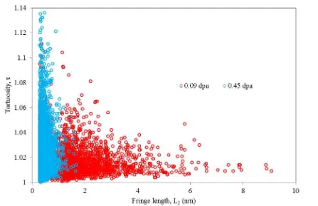
Data extracted from the fringe detection algorithm illustrated in Figure 5 (c) and (g)
of a fringe to its direct end-to-end length). Figure 6, shows that for low doses where the
structure is still ordered, the tortuosity of each detected fringe is relatively low, with over
75% having a tortuosity of 1 – 1.03 and a fringe length which is relatively high, extending to
8.9 nm. However when the structure becomes disordered following electron irradiation, the
tortuosity increases significantly, with highs of nearly 1.14, and the (002) fringes break up
[image:13.595.79.526.206.495.2]into shorter lengths, 98% of which are below 1 nm in length.
Figure 6 Comparison of fringe length and tortuosity data for the same region of interest having received low (red) and high (blue) electron irradiation doses.
A second-order (i.e. pairwise) statistical analysis of the orientation maps provides
information about the relative orientation of neighbouring fringes. Referring to the schematic
in Figure 7, the angles of planes to the vertical axis ( 1) were measured every 0.033 nm (pixel
resolution) from the origin for a set of radii (r) up to a maximum of 4 nm. Data at each angle ( ) were then plotted on a graph of mean orientation difference ( ) versus distance to determine the average opening angle for the 4 nm domain as shown in Figure 7. The mean
misorientation of the fringes corresponds to the plateau of the plots [39]. For example, the
plot taken at 0.7 dpa plateaus at max = 8.7° for both = 0° and 90° (the two extremes of ).
The plateau is reached by the = 0° data before the = 90° data implying there is a quicker loss of orientation in the a-axis ( = 0°) and domains are wider in the c-axis ( = 90°). This
exposure to produce a series of orientation maps and a plot of orientation angle against
electron dose (Figure 8). As expected it suggests that the relative orientation of planes
increases with electron irradiation, but appears to plateau at high doses, suggesting there is a
misorientation limit, potentially associated with the unstable transition from strained sp2
bonding to sp3 interlayer bonding. Although both data sets plateau at different values of ,
[image:14.595.100.485.203.406.2]they exhibit a similar trend suggesting there is a degree of short range homogeneity.
Figure 7 Change in mean orientation difference with distance from origin (r) at = 0° and = 90° following an electron dose of 0.7 dpa ± 6.4 %. The coherence lengths can be defined as the distance at which 90% of the value of the plateau is reached for the diagrams at 0° and 90° [39].
Figure 8 Change in mean orientation difference plateau, max, with electron irradiation for
[image:14.595.95.472.505.716.2]3.2 EELS
The bulk + valence plasmon peak in the low loss region of the spectrum was analysed; the position of the peak being determined by taking the first derivative of the spectrum. The
widely agreed value for the bulk plasmon peak position of highly oriented pyrolytic graphite
(HOPG) in the literature is 27 eV [40–43] (for comparison, the corresponding value for
amorphous carbon is 23 eV). As illustrated in Figure 9, the plasmon peak energy for PGA
graphite is consistently lower than that of HOPG. This may be due to the misorientation of
the specimen’s c-axis relative to the normal of the incident beam [44], in combination with
the choice of the spectrometer collection angle [14,45]. During the experiments the position
of the plasmon peak appears unchanged, or perhaps slightly decreases, as a function of dose
[image:15.595.90.510.325.538.2]to within experimental error.
Figure 9 Change in plasmon peak position with dose. Data are averaged over two regions of electron transparent (002) oriented PGA graphite. The error bars reflect the experimental variance. Dose error = ± 6.4%
A representative set of EELS C K-edge spectra as a function of electron irradiation is
presented in Figure 10 (a)-(d). The * peak maximum of all spectra was calibrated to 285 eV,
and C K-edge spectra were acquired every 90-100 seconds along with the corresponding low
loss peak which was used to deconvolute each K-edge spectra to remove plural scattering.
The data extracted from the spectrum acquired at t=0 were used to normalise subsequent sp2
(Figures 3-8), the presence of the * peak indicates that the structure retains a distinct sp2
[image:16.595.83.398.139.558.2]character.
Figure 10 Change in EEL spectra with dose (D): (a) D = 0 dpa; (b) D = 0.113 dpa; (c) D = 0.209 dpa; (d) D = 0.267 dpa ± 6.4%
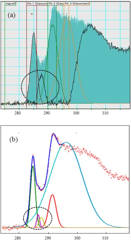
To characterise the ratio of (planar) sp2 bonded carbon to total carbon, an improved
automated fitting routine for the C K-edge was achieved by inclusion of two additional
Gaussian curves to the method proposed by Zhang [28] which employed three Gaussian
peaks (Figure 11 (a)): G1 centred at ~285 eV for the C=C * component; G2 ~292 eV, the
C-C * component and G3 ~300 eV, the C-C=C-C * component. The additional Gaussians were
uncertain origin: either from the presence of additional heterospecies (e.g. O or H) or the
presence of a non-planar sp2-bonded (fullerene-like) carbon component, as is the case here.
Figure 11 (a) Circled residual peak signal from a 3 Gaussian fit performed in Gatan Digital Micrograph (b) Circled residual peak signal from a 5 Gaussian fit performed in Hyperspy. The residual peak from (a) was deconvoluted into two separate peaks in (b).
All five Gaussians were fitted simultaneously using the following constraints:
- the first Gaussian (G1) centred at ~284.5 eV (with a constraint on the FWHM ( ): 0.25 eV ≤ ≤ 2 eV);
- second Gaussian (G2) centred at ~291.75 eV (2.1 eV ≤ ≤ 3.0 eV);
- third Gaussian (G3) centred at ~297.75 eV (11.2 eV ≤ ≤ 13.1 eV).
While for fitting the extra two Gaussians (G4 and G5), the script fixed the FWHM and the
centre of G1, G2 and G3 along with the area of G2 and G3, but allowed the area of G1 to
vary in order to accommodate the new components, which were then fitted using the
[image:17.595.71.283.126.520.2]- G4 centred at ~286.5 eV (0.2 eV ≤ ≤ 1.5 eV)
- G5 centred at ~288.5 eV (0.2 eV ≤ ≤ 1.5 eV).
The variation of planar sp2 content was calculated by comparing the ratio of the *
intensity (G1) with the total C K-edge intensity (over a 20 eV window of onset 282.5 eV)
which is proportional to the total number of carbon atoms present in the probed volume:
Planar content
I I
I
I Equation 3.1
where the intensity values from the initial C K-edge spectrum were used to calculate (I * /
I *+ *)t=0 so as to ensure all spectral changes were relative to the initial structure. As can be
seen in Figure 12 the sp2 content changed approximately linearly with respect to electron
dose. The sp2 content dropped to 76% following an exposure of 0.32 dpa, a value consistent
with the typical value of 75% sp2 carbon derived from an amorphous carbon film using this
fitting method. These changes provide evidence for the introduction of atomic disorder as a
result of electron beam exposure. The errors shown in Figure 12 reflect an analytical error of
± 6% (determined by making slight changes to the energy windows to account for subjective
[image:18.595.87.513.471.695.2]discrepancy) and the variation in data between four separate experiments.
graphite. The error bars reflect the experimental variance and analytical error. Dose error = ± 6.4%
The signals from the G4 and G5 peaks were also analysed to provide information
regarding the non-planar sp2 carbon content of the specimen by measuring the ratio between
the combined intensities under G4 and G5 (IR) and the combined intensities under the G4, G5
and G1 peaks (IR+sp2), as detailed in Equation 3.2. This ratio is proportional to the fraction of
sp2-bonded carbon atoms which are bonded in a non-planar fashion and the increase in this
quantity with increasing electron dose is plotted in Figure 13. Note the non-zero value of this
quantity at zero-extrapolated dose is due to the inherent intensity in this spectral region (even
in a pure planar sp2 carbon based material) as well as any non-planar sp2 carbon atoms
[image:19.595.97.501.358.645.2]located at crystallite grain boundaries within the analysed volume. Comparing the data in
Figure 12 and Figure 13, it appears as though the loss of planar sp2 bonding (very roughly a
20% decrease) is predominantly accounted for by an increase in non-planar sp2 bonded
carbon.
Non planar s Equation 3.2
Figure 13 Change in non-planar sp2 content with dose over two regions of electron transparent (002) oriented PGA graphite. Error bars reflect experimental variance and analytical error. Dose error = ± 6.4%
Taking the first derivative of the C K-edge spectrum to analyse the change in the MSR
peak position during the electron beam damage series, we observe a slight decrease in energy
increases for higher doses where the MSR peak becomes wider leading to a degree of
uncertainty in peak energy assignment; the error bars in Figure 14 represent experimental
variation. Results obtained by Daniels [27] following a series of graphitization experiments
are analogous, whereby the graphite began as a highly disordered material with an average
bond length of 1.435 Å and through annealing became a near-perfect structure with a
corresponding bond length of 1.420 Å. In Daniels’ case, the decrease in bond length during
graphitization was attributed to a decrease in sp3 bonding (bond length = 1.54 Å) and the
removal of heteroatoms and aliphatic molecules (bond length > 1.42 Å). In the present case
however, no heteroatoms and aliphatic molecules are introduced to the system and the high
energy barrier between graphite and diamond phases makes sp2 to sp3 transformation unlikely
unless at very high temperature (~1000 K) [46]. However, we have established that the
electron irradiation induces nanocrystallinity with atomic disorder at crystallite grain
boundaries, (Figure 2 and 7), and it is this disorder that reduces the packing efficiency of
carbon atoms which is thought to increase the average bond length (e.g. for the most extreme
case of amorphous carbon, the bond length increases to 1.44 Å [47]). It is thus suggested that
introduction of dislocations and defects along with a bending of planes (the introduction of
non-six-membered rings of carbon atoms [21]) following electron irradiation increases the
average C-C bond length. One might expect that an increase in bond length would lead to a
reduction in valence electron density (and thus the possible slight reduction in plasmon
[image:20.595.89.508.509.715.2]energy with increasing dose as shown in Figure 9).
4 Final Discussion and Conclusions
We have presented a new methodology to quantitatively analyse TEM micrographs of
irradiation damaged graphite. Following electron irradiation at 200 keV, a decrease in the
graphite (002) fringe length and an increase in tortuosity and relative misorientation was
observed indicating a reduction in the alignment of basal planes. Analysis of the low and
core loss of several EEL spectral series indicates little or no change in valence electron
density, a decrease in planar sp2 content (to levels associated with amorphous carbon at the
highest doses), an increase in non-planar sp2 content (of inverse proportion to the planar sp2
reduction and an increase in C-C bond length, all reflecting an increasing tortuosity of (002)
layer planes and an increasing nanocrystallinity upon exposure to an increasing electron dose.
Future work will involve the application of this analysis methodology for radiation
damage to electron-irradiated samples at nuclear reactor temperatures (400°C) as well as
neutron-irradiated samples from nuclear reactors and materials test reactors. The full
potential of the image analysis software provided by the PyroMaN research group will also
be investigated.
Acknowledgements
This paper was written by Brindusa Mironov and Helen Freeman. Funding was provided by
the National Nuclear Laboratory and EPSRC (grants EP/J502042/1 and EP/I003312/1). We
acknowledge Abbie Jones of the University of Manchester, UK, for the provision of polarised
light micrographs and Anne. A. Campbell at the University of Michigan, U.S.A, for the
provision of the Graphite Anisotropy Analysis Program (GAAP). Fred S. Hage would like to
acknowledge Magnus Kristofer Nord (Norwegian University of Science and Technology,
Trondheim, Norway) for assistance and useful discussions when setting up the C-K edge
fitting procedure in HyperSpy (freely available from http://hyperspy.org/). SuperSTEM is the
UK Engineering and Physical Sciences Research Council (EPSRC) National Facility for
aberration-corrected STEM. Jean-Pierre Da Costa and Patrick Weisbecker acknowledge
support from the ANR agency through a grant to the program "PyroMaN"
References
[1] Department of Energy & Climate Change (DECC). Table of past and present nuclear reactors in the UK. London: 2014.
[2] Nightingale RE. Nuclear Graphite. Academic Press Inc.; 1962.
[3] Wen K, Marrow J, Marsden B. Microcracks in nuclear graphite and highly oriented pyrolytic graphite (HOPG). Journal of Nuclear Materials 2008;381:199–203.
[4] Hennig GR. Vacancies and dislocation loops in graphite. Applied Physics Letters 1962;1.
[5] Thrower PA, Reynolds WN. Microstructural changes in neutron-irradiated graphite. Journal of Nuclear Materials 1963;8:221–6.
[6] Bollmann W, Hennig GR. Electron microscope observations of irradiated graphite single crystals. Carbon 1964;1:525–33.
[7] Heggie MI, Suarez-Martinez I, Davidson C, Haffenden G. Bukled, ruck and tuck: A proposed new model for the response of graphite to neutron irradiation. Journal of Nuclear Materials 2011;413.
[8] Mitchell EWJ, Taylor MR. Mechanism of stored-energy release at 200°C in electron irradiated graphite. Nature 1965;208:638–41.
[9] Ohr SM, Wolfenden A, Noggle TS. Electron displacement damage in graphite and aluminium. In: Thomas G, Fulrath RM, Fisher RM, editors. Electron Microscopy and Microstructure of Materials, University of California Press; 1972, p. 964.
[10] Thrower PA, Mayer RM. Point defects and self-diffusion in graphite. Physica Status Solidi (a) 1978;47:11–37.
[11] Yazyev O, Tavernelli I, Rothlisberger U, Helm L. Early stages of radiation damage in graphite and carbon nanostructures: A first-principles molecular dynamics study. Physical Review B 2007;75:115418.
[12] El-Barbary AA, Trasobares S, Ewels CP, Stephan O, Okotrub A V, Bulusheva LG, et al. Electron spectroscopy of carbon materials: experiment and theory. Journal of Physics: Conference Series 2006;26:149–52.
[13] Simmons JHW. Radiation damage in graphite. vol. 102. Pergamon Press; 1965.
[14] Egerton RF. Electron Energy-Loss Spectroscopy in the Electron Microscope. 3rd ed. Springer; 2011.
[16] Baker DE. Graphite as a neutron moderator and reflector material. Nuclear Engineering and Design 1970;14:413–44.
[17] Trevethan T, Dyulgerova P, Latham CD, Heggie MI, Seabourne CR, Scott AJ, et al. Extended Interplanar Linking in Graphite Formed from Vacancy Aggregates. Phys Rev Lett 2013;111:95501.
[18] Goggin PR, Henson RW, Perks AJ, Reynolds WN. Dimensional changes in the irradiated graphite lattice. Carbon 1964;1:189–200.
[19] Henson RW, Perks JA, Simmons JHW. Lattice parameter and dimensional changes in graphite irradiated between 300 and 1350°C. Carbon 1968;6:789–806.
[20] Brocklehurst JE, Kelly BT. Analysis of the dimensional changes and structural changes in polycrystalline graphite under fast neutron irradiation. Carbon 1992;31.
[21] Karthik C, Kane J, Butt DPP, Windes WEE, Ubic R. In situ transmission electron microscopy of electron-beam induced damage process in nuclear grade graphite. Journal of Nuclear Materials 2011;412:321–6.
[22] Mileeva Z, Ross DK, King SM. A study of the porosity of nuclear graphite using small-angle neutron scattering. Carbon 2013;64:20–6.
[23] Mrozowski S. Mechanical strength, thermal expansion and structure of cokes and carbons. Proceedings of the Conferences on Carbon 1954:31.
[24] Hall G, Marsden BJ, Fok SL. The microstructural modelling of nuclear grade graphite. Journal of Nuclear Materials 2006;353:12–8.
[25] Windes W, Burchell T, Bratton R. Graphite Technology Development Plan. 2007.
[26] Banhart F. Irradiation effects in carbon nanostructures. Reports on Progress in Physics 1999;62:1181–221.
[27] Daniels HR, Brydson R, Rand B, Brown AP. Investigating carbonization and graphitization using electron energy loss spectroscopy (EELS) in the transmission electron microscope (TEM). Philosophical Magazine 2007;87:4073–92.
[28] Zhang Z, Brydson R, Aslam Z, Reddy S, Brown AP, Westwood A, et al. Investigating the structure of non-graphitising carbons using electron energy loss spectroscopy in the transmission electron microscope. Carbon 2011;49:5049–63.
[29] Daniels H, Brown AP, Scott A, Nichells T, Rand B, Brydson R. Experimental and theoretical evidence for the magic angle in transmission electron energy loss spectroscopy. Ultramicroscopy 2003;96:523–34.
[31] Oen OS. Cross sections for atomic displacements in solids by fast electrons. ORNL- 3813. Oak Ridge National Laboratory; 1965.
[32] Krasheninnikov A V, Nordlund K. Ion and electron irradiation-induced effects in nanostructured materials. Journal of Applied Physics 2010;107:071301.
[33] Takeuchi M, Muto S, Tanbe T. Structural change in graphite under electron irradiation at low temperatures. Journal of Nuclear Materials 1999;271&272:280–4.
[34] Scherzer O. The theoretical resolution limit of the electron microscope. Journal of Applied Physics 1949;20:20.
[35] Campbell AA, Was GS. In situ proton irradiation-induced creep at very high temperature. Journal of Nuclear Materials 2013;433:86–94.
[36] Raynal PI, Monthioux M, Da Costa J-P, Dugne O. Multi-scale quantitative analysis of carbon structure and texture: III. Lattice fringe imaging analysis. In: American Carbon Society, editor. Proceedings of Carbon, Clemson, South Carolina, USA.: Curran Associates, Inc.; 2010, p. 873–4.
[37] Da Costa J-P, Germain C. Level curve tracking algorithm for tectural features extraction. Pattern Recognition, 2000 Proceedings 15th International Conference on 2000;2:909–12.
[38] Farbos B, Weisbecker P, Fischer HE, Da Costa J-P, Lalanne M, Chollon G, et al. Nanoscale structure and texture of highly anisotropic pyrocarbons revisited with transmission electron microscopy, image processing, neutron diffraction and atomistic modeling. Carbon 2014;80:472–89.
[39] Da Costa J-P, Weisbecker P, Farbos B, Leyssale J-M, Vignoles G, Germain C. Investigating carbon materials nanostructure using image orientation statistics. Carbon 2014;Submitted.
[40] Henrard L, Stephan O, Colliex C. Electron Energy Loss study of plasmon excitation in curved carbon network. Synthetic Metals 1999;103:2502–3.
[41] Laffont L, Monthioux M, Serin V. Plasmon as a tool for in situ evaluation of physical properties for carbon materials. Carbon 2002;40:767–80.
[42] Gass MH, Bangert U, Bleloch AL, Wang P, Nair RR, Geim AK. Free-standing graphene at atomic resolution. Nature Nanotechnology 2008;3:676–81.
[43] Egerton RF. Electron energy-loss spectroscopy in the TEM. Reports On Progress In Physics 2009;72:016502.
[44] Marinopoulos A, Reining L, Olevano V, Rubio A, Pichler T, Liu X, et al. Anisotropy and Interplane Interactions in the Dielectric Response of Graphite. Physical Review Letters 2002;89:076402.
[46] Banhart F. The role of lattice defects in the formation of new carbon structures under electron irradiation. Japanese Society of Electron Microscopy 2002;51:189–94.