promoting access to White Rose research papers
White Rose Research Online
[email protected]
Universities of Leeds, Sheffield and York
http://eprints.whiterose.ac.uk/
This is a copy of the final published version of a paper published via gold open access
in
Journal of the American Ceramic Society
This open access article is distributed under the terms of the Creative Commons
Attribution Licence (
http://creativecommons.org/licenses/by/3.0
), which permits
unrestricted use, distribution, and reproduction in any medium, provided the
original work is properly cited.
White Rose Research Online URL for this paper:
http://eprints.whiterose.ac.uk/87549
Published paper
Heath, J.P., Dean, J.S., Harding, J.H. and Sinclair, D.C.J. (2015)
Simulation of
impedance spectra for core-shell grain structures using finite element modeling
.
Journal of the American Ceramic Society, 98 (6). 1925 - 1931.
Simulation of Impedance Spectra for Core
–
Shell Grain Structures Using
Finite Element Modeling
James P. Heath, Julian S. Dean,
†John H. Harding and Derek C. Sinclair
Department of Materials Science & Engineering, University of Sheffield, Sir Robert Hadfield Building, Mappin Street, Sheffield S1 3JD, UK
The volume fraction of core- and shell-regions is an important parameter in the control of temperature-dependent electrical properties of core–shell-microstructured electroceramics such as BaTiO3. Here, we highlight the potential unreliability of
using capacitance ratios, obtained by simulating impedance spectra, to extract accurate volume fractions of the two regions. Two microstructures were simulated using a finite ele-ment approach: an approximation to a core–shell structure (the encased model) and a series-layer model (SLM). The imped-ance response of the microstructures was simulated for a range of input volume fractions. The volume fractions obtained from the simulation agreed with the input values for the SLM micro-structure but differed for the encased model. Current density and electric field plots revealed that this discrepancy was caused by differences between the physical and electrical micro-structures of the encased model. A stream trace analysis of current density demonstrated that the current follows the path of least resistance through the core, leaving regions of shell with lower current density. These differences are important when attempting to extract volume fractions from encased microstructures with small cores. In the present case, core volume fractions less than 0.7 produce differences in excess of 25%.
I. Introduction
I
MPEDANCEspectroscopy (IS) is a well-established techniqueto probe the electrical properties of a wide range of mate-rials1 and devices.2 By measuring impedance spectra over a wide-frequency range, it is often possible to identify and characterize electrically distinct regions, for example, bulk and grain-boundary components in electroceramics. To sepa-rate different components or processes requires differences in their characteristic relaxation times (or time constants) of at least two orders of magnitude within the measured frequency range.
Ferroelectric BaTiO3-based ceramics form the cornerstone of the multilayer ceramic capacitor (MLCC) industry with over 2 trillion units produced each year.3 Achieving the required 15% temperature coefficient of capacitance (TCC) for X7R and X8R4capacitors requires control of pro-cessing conditions to create electrically heterogeneous grains with a core–shell microstructure. The core regions are un-doped-BaTiO3(Curie temperature~125°C), whereas the shell (outer) regions contain a distribution of dopants that alter electrical properties (electrical conductivity, r, and relative permittivity,er) and lower the Curie temperature. Jeonet al5
showed that a shell thickness of about a third of the core
radius is needed to obtain satisfactory TCC behavior for (Mg, Y) codoped BaTiO3 using a combination of transmis-sion and scanning electron microscopy (TEM, SEM) with fixed-frequency dielectric measurements. As BaTiO3 is sensi-tive to dopants and contaminants, the core/shell ratio required depends on the dopants and dopant couples used. Moreover, the electrical microstructure may differ from the physical microstructure obtained by measurement of the dop-ant concentration. Further microstructural characterization is needed to optimize BaTiO3-based MLCCs. We have charac-terized the core and shell volume fractions in commercial positive temperature coefficient of resistance thermistors based on BaTiO36 using IS. Analysis using complex electric modulus plots and spectroscopic plots of the imaginary com-ponent,M″, of the electric modulus suggested that the shell regions were about 20% of the thickness of the core regions. This was confirmed by conductive atomic force microscopy that revealed Schottky barrier regions of ~500 nm for an average grain size of~5lm.7
There has been recent interest in the incipient ferroelectric perovskite CaCu3Ti4O12 (CCTO) due to the high and tem-perature stable capacitance behavior of CCTO ceramics at radio frequencies near room temperature. It is now widely accepted that this effect is due to electrical heterogeneity aris-ing from semiconductaris-ing grains and insulataris-ing grain bound-aries for samples processed at ~1100°C.8,9 Between the extreme processing conditions of 700°C and 1100°C, where insulating and semiconducting grains were clearly revealed by separate peaks inM″spectroscopic plots, the volume frac-tions of the two phases were estimated from changes in the
M″ peak heights assuming a microstructure with a conduc-tive core and an insulating shell.10 A similar relationship between volume fractions of Suzuki phases in NaCl, using
M* arc diameters instead of M″ peak heights, has been reported by Bonanos and Lilley.11
These examples show that IS is potentially an easy and reliable technique to quantify core/shell volume fractions but we need to know when it can be employed to characterize the electrical properties of core and shell regions in micro-structures. The analyses described above are crude extensions of the brick-work layer model (BLM)12used to identify bulk (grain) and grain-boundary responses in electroceramics. In the BLM, an equivalent circuit based on two parallel resis-tor-capacitor (RC) elements connected in series is used to analyze IS data. One element represents the grain response (RbCb) and the other represents the grain-boundary response (RgbCgb). Both give arcs in complex impedance (Z*) and electric modulus (M*) plots and Debye peaks in Z″ andM″
spectroscopic plots.
The BLM assumes that: all grains are cubic, isotropic and are separated by thin, resistive, regular grain-boundary regions (Rgb≫Rb and Cgb≫Cb); the relative permittivity,
er, of the grain and grain-boundary regions is the same; the time constant,s=RC for the regions differs by at least two orders of magnitude allowing the responses to be resolved in the IS data. The capacitance for each region is a function of
D. J. Green—contributing editor
Manuscript No. 36020. Received December 4, 2014; approved January 28, 2015.
†Author to whom correspondence should be addressed. email: j.dean@sheffield.ac.uk
1925
DOI: 10.1111/jace.13533
©2015 The Author.Journal of the American Ceramic Societypublished by Wiley Periodicals, Inc. on behalf of American Ceramic Society (ACERS) This is an open access article under the terms of the Creative Commons Attribution License, which permits use, distribution and reproduction in any medium, provided the original work is properly cited.
their respective thicknesses for a fixed electrode area and can be calculated from the arc diameters in M*plots. The vol-ume ratio of bulk to grain-boundary regions is estimated as the ratio Cb/Cgb.
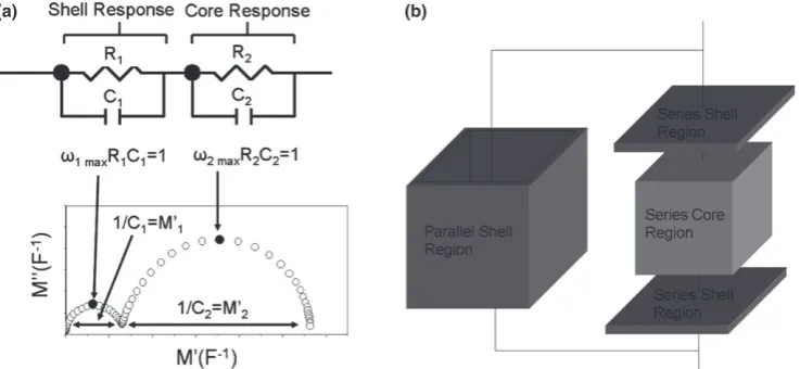
To test this analysis, we used the BLM of a dual RC cir-cuit to simulate the IS response of grain shell (R1C1) and grain core (R2C2) regions, as shown in Fig. 1(a). The resistiv-ity of the shell region is assumed to be three orders of magni-tude greater than the core anderis assumed to be the same for both regions. The volume fraction of the core region,
/core, is estimated from the M* arc diameters using the expression10:
/core¼
M02
M01þM02 (1)
where/core is the core region volume fraction, andM01and
M02are the arc diameters corresponding to the shell and core regions, respectively, as shown in Fig. 1(a). Varying the core–shell volume fraction strongly affects how the current flows through this microstructure. The current must pass through the region of the resistive shell in series with the conductive core region and the electrodes but it may avoid regions of the shell in parallel with the core [see Fig. 1(b)], leading to an inhomogeneous current density within the microstructure. If the shell region in parallel with the core is less electrically active than the core, it will not contribute sig-nificantly to the impedance response, giving a discrepancy between the true volume fractions of the regions and those measured using an M* plot. Inhomogeneous current density within the microstructure will influence the R and C values extracted for the core and shell regions.
Kidner et al13 have reviewed a good selection of tech-niques used to model IS of electroceramics. Some, like effec-tive medium theory (EMT), are analytically solvable.14 Others, based on Bauerle’s BLM,12 employ large resistor/ capacitor networks and require a numerical solution. Here, we compare a conventional BLM analysis for IS data with a finite element model (FEM).
II. Finite Element Method
We have developed a code15 that uses Maxwell’s equations16 to solve the electrical response of the system directly for an arbitrary microstructure. The package can consider a full physical microstructure including (but not limited to) grain cores, grain shells, grain boundaries, and electrode contacts. This can include randomized, nonuniform microstructures but we focus here on the validity of extending the BLM
approach to core–shell microstructures. Each region can be assigned material properties independently. This permits all the geometrical and material properties of the physical microstructure to be specified: core–shell volume fractions and their respectiverandervalues. Similar approaches have been used in 2D modeling17 however, hitherto 3D models have been limited in their complexity.18
The simple physical microstructures discussed above can be controlled by altering the volume fraction of the core and shell regions. The geometry of the physical microstructure is produced using Voronoi tessellation.19 First, the required grain shapes are generated. Subgrain features are then pro-duced by shrinking the grain, leaving a volume for the shell region. All regions are then meshed with tetrahedral elements using the program Gmsh.20 The corresponding electrical
microstructure is determined by analyzing the simulated IS response and comparing with that assumed by the BLM. We assume that both phases haveer=100 and the shell conduc-tivity (0.1lS/cm) is three orders of magnitude lower than the core conductivity (100lS/cm). More realistic scenarios (e.g., noncubic grain microstructures; larger variations in per-mittivity and conductivity between the components) will be considered in future work.
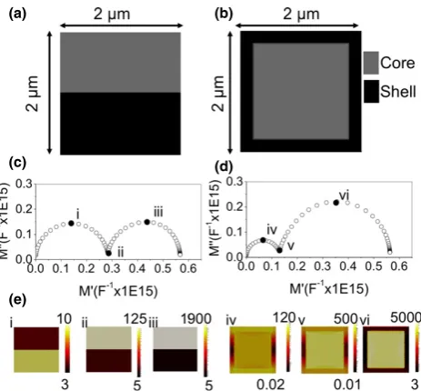
Two microstructures are considered. The first is Maxwell’s series layer model (SLM),16 consisting of layers of shell and core regions connected in series with the layer normals paral-lel to the applied voltage difference [Fig. 2(a)]. The second is a core–shell microstructure, shown in Fig. 2(b), consisting of nested cubes where the inner region is the core. This will be referred to as the encased model.
A range of volume fractions for the core region was used for both cases while keeping the material properties constant. The core and shell thicknesses for several core volume frac-tions (for both models) are listed in Table I. The distance between the electrode contacts was 2lm. The mesh size was set from a convergence study at 20 000 nodes and over one million elements. The IS response of each model was simu-lated over the range 1 Hz to 0.1 GHz. At present the model simulates a linear (ohmic) current–voltage relationship. An arbitrary potential difference of 100 V was applied across the model by setting a Dirichlet boundary condition at the top and bottom of the model. All other external surfaces are assigned a Neumann boundary condition to confine the cur-rent inside the model. The IS data generated were plotted in
Z*andM*formalisms using the programZplot.21
3D representations of the current density, electric field, or electric potential were overlaid on the physical microstructure of the models to facilitate direct comparison. We use the cur-rent density distribution to identify regions that contribute significantly to the impedance response. The current density
[image:3.595.101.470.563.733.2](a) (b)
Fig. 1. (a) Schematic of an M* plot for a dual RC circuit with intercepts. (b) Schematic of a brick layer representation of a core–shell microstructure.
plots are taken at frequencies that correspond to the M″
maxima onM*plots at the maximum applied voltage. These show the highest concentrations of current density in the shell and core regions (the low and high-frequencyM″ max-ima, respectively) relative to the rest of the model and permit the electrical microstructure to be compared with the physi-cal microstructure. Electric field plots taken at the same point are used to examine the relationship between electric field and current density.
To analyze the current density plots, the conduction path-ways through the model are plotted using a stream trace22 analysis of the current density vector field produced by the program ParaView.23 This gives the conduction pathway through the model by calculating the curl of the current den-sity. An array of 19 by 19 stream tracer seed points was placed on the bottom electrode surface and the length of each trace measured. The standard deviation of the traces provides the distribution of conduction path lengths (DCPLs).
III. Results
The impedance response for both the SLM and encased models was simulated for a range of core volume fractions. Output core volume fractions were extracted using Eq. (1)
and the results compared to the input values for both models. The SLM can be solved analytically and the output core volume fraction should be the same as the input value. This was used to validate the FEM code. It is also useful to compare the SLM response, the extracted R, C, s values, and the volume fractions of the core and shell regions with those of the encased model—where current flow will not be homogeneous except for the special cases/core =0 or 1.
M* plots of simulated IS data for the SLM and an encased structure (both with equal core and shell phase vol-ume fractions) together with inserted current density plots for various frequencies (i)–(vi) are shown in Fig. 2. TheM*
plots clearly demonstrate that the physical microstructure influences the IS response. For the SLM, theM*arc diame-ters are equal, as predicted for equal volume fractions. How-ever, for the encased model, the shell arc is less than a third of the size of the core arc. Unless the physical microstructure is known, the volume fraction of the core is over-estimated by extracting C from the corresponding M* arc (as M0
depends inversely on C). Likewise, the shell volume fraction is underestimated. For the encased model, the current density plots show regions of low current density in the parallel shell regions, as shown in Fig. 2(e) (iv). The current density is homogeneous within the individual core and shell layers for the SLM, as shown in Fig. 2(e) (i)–(iii).
For the SLM, the core volume fraction (/core) calculated from the M* plots of the simulated IS data was equal to the input value for all volume fractions. For the encased model, the calculated value of /core was larger than the input value, as shown in Fig. 3(a). The current bypasses the regions of the shell parallel to the core which do not con-tribute to the M* arcs. The Bonanos–Lilley equations11 describe how a cubic unit of the electrical response of a material modeled by Maxwell’s EMT can be equated to a dual RC circuit and were therefore used to provide an ana-lytical fit to this effect. The agreement between the results obtained from the Bonanos–Lilley equations and the encased model shows that the discrepancies in volume frac-tions are physically reasonable, as shown in Fig. 3. Although the difference between the input and output core fractions reduces at lower input fractions, expressing the output fraction as a percentage of the input value shows a much higher percentage deviation at smaller values of the input fraction, as shown in Fig. 3(b).
R and C values fromM*plots were obtained for the core and shell responses using the intercepts and the relationship
xRC=1, see Fig. 1(a). This gave s for the core and shell region of the SLM as 8.67 ls and 8.75 ms, respectively, for all/core. This agreed with the input material parameters used in the model. For the encased model,s for the shell region (sshell) was 8.75 ms for all volume fractions, whereas s for the core region (score) increased with decreasing /core. score (encased model) agreed with score (SLM) at /core =1 but started to increase significantly at /core ~0.8 up to ~5 score (SLM) at /core ~0.02, Fig. 4. Fitting semicircles to the M* arcs to calculate s for the core and shell regions revealed
(a) (b)
(c)
(e)
[image:4.595.66.298.40.255.2](d)
Fig. 2. (a) A schematic of the setup for the SLM and (b) for the encased model for Vcore=Vshell, see Dean et al15 for how this geometry can be modified to form a polycrystal. (c) Simulated IS data are shown asM* plots for the SLM and (d) for the encased model. (e) Current density plots are shown for each model at selected frequencies that coincide withM″inflexion points in theM*
[image:4.595.63.565.635.746.2]plot for the SLM (i)–(iii) and encased (iv)–(vi) models. All scales are logarithmic and in A/m2.
Table I. A List of 2D Measurements for the SLM and Encased Model for a Range of/coreor Volume Ratios (3D Measurements)
/core(%) Volume ratio (Vcore:Vshell)
SLM Encased
Shell thickness (lm) Core thickness (lm) Shell thickness (lm) Core thickness (lm)
0.02 1:49 1.96 0.04 0.729 0.543
0.1 1:9 1.8 0.2 0.536 0.928
0.2 1:4 1.6 0.4 0.415 1.170
0.5 1:1 1 1 0.206 1.587
0.65 13:7 0.7 1.3 0.134 1.732
0.8 4:1 0.4 1.6 0.072 1.856
0.98 49:1 0.04 1.96 0.007 1.987
more arc merging (greater uncertainty in the s values) at lower values of /core [see inserted M* plots, Fig. 4(i)–(iv)]. The maximum uncertainty was 30%, so this alone could not account for the substantial changes in score (encased model). The results in Fig. 4 imply a geometrical dependence in the value of score (encased model). This contradicts the expectation that s should be geometry independent due to cancellation of the R and C geometric terms.24
To further investigate the cause of this geometry-depen-dent effect, R and C values for the encased model (from the
high-frequency core and low-frequency shell response inM*
plots) were independently compared to those of the SLM. Except for the special cases /core=1 and 0, the resistance for the encased shell region (Rshell) was lower than Rshell for the SLM, Fig. 5(a). In contrast, the core resistance (Rcore) for the encased model was substantially higher than Rcorefor the SLM, Fig. 5(b). Rcore for the encased model showed an unusual trend with /core, Fig. 5(b). There was a linear increase in Rcorefrom /core=1.0 down to ~0.4, followed by a leveling-off down to/core ~0.2 and finally a steep, nonlin-ear decrease toward the SLM value at/core~0. This suggests a transition in the conduction behavior for the model associ-ated with core–shell microstructural effects, especially for
/core <0.4. Capacitance values for both regions and models had a similar form, increasing as the respective components became thinner. This suggests the enhancement of score (encased model) at low/core is related to conduction path-ways through the core phase.
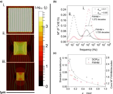
For the encased model, the distribution of conduction path lengths DCPLs at the high-frequency Debye response (for the core region at the frequency associated with theM″
maximum) for a range of input /core values was obtained using methods described previously. The corresponding cur-rent density plots show heterogeneous curcur-rent flow through the grains with a larger current density in the conductive core. This shows that the current follows the path of least resistance, in good agreement with theory and other com-puter modeling studies.15,25,26When/
coreis large, the current flowing through the encased core is almost homogenous but it becomes increasingly heterogeneous as /core decreases, Fig. 6(a) (i)–(iii). The full-width half maximum (FWHM) value of the M″ peak associated with the encased core response was also measured, as shown in Fig. 6(b). Compari-son between the FWHM and values for the DCPLs shows that a broader path length distribution correlates to a broader M″ Debye peak, Fig. 6(c). The broadening of the DCPLs is caused by increased curvature of the path lengths at lower/core values. The current density plots and overlaid conduction paths, Fig. 6(a) (i)–(iii), are 2D slices extracted from the full 3D dataset. However, the path length statistics were calculated from the 3D model and not just the plots shown in Fig. 6.
IV. Discussion
The simulations for the SLM and encased models highlight the significance and relationship between their physical and electrical microstructures, their influence on the impedance spectra produced and the applicability of the encased cubic grain model to assess core–shell volume fraction in ceramics. The SLM results in Figs. 2, 3, and 5 validate our FEM. They show that s is independent of the chosen geometry for all values of /core for both the core and shell regions. As expected, the magnitude of the current density in the two regions is generally different and frequency dependent. The behavior at /core=0.50 [Fig. 2(e) (i)] shows high current density in the resistive shell region at low frequency, whereas higher current density occurs in the conductive core region at high frequency, Fig. 2(e) (iii). Assshell =1000score,the maxi-mum value of M″ for the shell occurs at much lower fre-quency than for the core and the two responses are well resolved inM*plots, Fig. 2(c). The current density is homo-geneous within each region, for all values of /core and fre-quency, Fig. 2(e) (i)-(iii). For the SLM, this allows reliable extraction of core volume fraction and R, C,sas a function of the input core fraction/coreas shown in Figs. 3(a) and 5, respectively.
The results for the encased model in Figs. 2, 3, and 5 show the problems in extending the BLM to core–shell struc-tures. The most obvious is the dependence of score on /core for a wide range of/corevalues (in Fig. 4, for/core<0.8, and our chosen values forr ander). When/core=0.50 (Fig. 2),
(a)
[image:5.595.66.234.40.249.2](b)
Fig. 3. (a) Output volume fraction plotted against input volume fraction for: the Bonanos–Lilley equations (i), the encased model (ii), and the SLM (iii). (b) The percentage deviation in output volume fraction from assigned values plotted against input volume fraction for cases (i) and (ii) above.
Fig. 4. (top) Calculatedsvalues for the core phase obtained from the analysis of M* spectra plotted against/core for the SLM and encased models.M*plots (i)–(iv), show an increase in arc merging with decreasing/core.
[image:5.595.34.272.316.593.2](a) (b)
[image:6.595.128.493.45.321.2](c) (d)
Fig. 5. (a) Extracted shell resistance, (b) core resistance, (c) shell capacitance, and (d) core capacitance for a range of input values of/corefor the SLM and encased models. Inserts in (c) and (d) are an enlargement showing the change in/corevalues at lower capacitance.
(a) (b)
(c)
(
j
)
[image:6.595.131.500.365.669.2]the change in physical microstructure from the SLM to the encased model clearly has a dramatic influence on the M*
[image:7.595.99.463.519.726.2]response. This is shown by comparing Figs. 2(c) and (d), the volume fractions obtained from the ratios of the M* arc diameters and the current density behavior observed [Fig. 2(e)] within the core and shell regions. This has signifi-cant consequences for the electrical microstructure of the encased model.
The current density plots in Fig. 2(e) explain the discrep-ancy between the volume fractions calculated from the simu-lated IS data in Fig. 2(d) and the input values for the encased model. Although the variation in the current density with frequency is similar in the encased model to the SLM, the current density is no longer homogenous within each region. Figure 2(e) (iv) shows the current to take the path of least resistance when presented with a choice of flowing through the (conductive) core or the (resistive) shell for the encased model. This leads to a lower current density in the shell region parallel to the core, reducing its contribution to the magnitude of the impedance response. This loss of effec-tive thickness in the shell region increases the measured capacitance, which gives a smaller shell (low frequency) M*
arc diameter in Fig. 2(d). Using Eq. (1) to estimate volume fractions from M* arcs therefore underestimates the shell volume fraction and hence overestimates the core as our sim-ulations are performed for a constant grain volume. As the core fraction decreases, the error in the core fraction esti-mated fromM*spectra increased to over 250% [in Fig. 3(b) for /core=0.02]. The error in the extracted core fraction exceeds 25% for/core<0.7.
Another approach would be to insert extracted capaci-tance values into the Bonanos–Lilley equations to predict the volume fractions of the regions. This has previously been tried by Kidneret al.13,27However, this approach still under-estimates /core because the BLM assumes nested cubes, whereas the Bonanos–Lilley equations, being derived from EMT, assumes nested spheres. A cube is more intrinsically conductive than a sphere assuming both shapes are the same material and volume.28Any simulations undertaken therefore require the correct physical shape of the microstructure to ensure results obtained from the simulated IS data are rele-vant and meaningful.
Although the shell region parallel to the core in the encased model has a much lower current density than the rest of the model, it is not zero. Furthermore, with
decreasing /core the area of the shell region parallel to the core presented to the incoming current increases, reducing its effective resistance. Using the stream trace analysis of the current density vector field we highlight two conduction path-ways at low/core, Fig. 6(a) (i)–(iii). First, there is a long con-duction path that curves more strongly toward the core as
/core is reduced. Second, there is a short conduction path that goes straight through the parallel shell phase. A statisti-cal analysis of the conduction path lengths for a range of vol-ume fractions showed that the distribution of the conduction path lengths broadens as /core decreased. Measuring the FWHM of the high-frequency (core) M″ Debye peak revealed that both the core FWHM and the standard devia-tion of the distribudevia-tion of the conducdevia-tion path lengths increases as/core decreases, Fig. 6(b). A secondary effect of the increased curvature of the long conduction pathways was the increased heterogeneity of the current density within the core, leading to the unusual conduction behavior and Rcore values shown in Fig. 4, and the dependence of score on the geometry, Fig. 5(b).
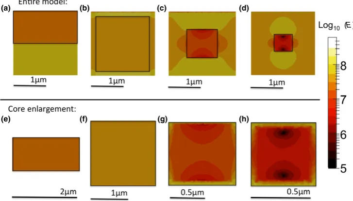
These unusual core effects can be analyzed by inspecting variations in the electric field experienced by the core and shell regions in both the SLM and encased models. For both models the electrode area and cube volume are fixed for all /core. In all cases, the current density spreads later-ally through the region in series with the electrodes to mini-mize overall resistance. This is in good agreement with a previous modeling study.25For the SLM, the core and shell regions are connected only in series and therefore the elec-tric field remains homogeneous in each region, Fig. 7(a). In this model, the physical and electrical microstructure are identical and any change in the physical microstructure aris-ing from a change in /core will be reflected in the electrical microstructure and can be readily analyzed using IS data.
Due to the coexistence of series and parallel pathways in the encased model, the electric field experienced by the core region depends on both the physical microstructure (dimen-sions and morphology) and the material properties of the two phases. In the present model, where the cores are cubes andrcore=1000rshell;er,core=er,shell, the electric field experi-enced by the core changes with /core. For /core≥0.65 the electric field (and current density) experienced by the core is reasonably homogeneous, Fig. 7(b), as the shell region paral-lel to the core is thin with a high effective resistance. The electrical microstructure therefore remains similar to the
(a)
(e) (f) (g) (h)
(b) (c) (d)
(E)
Fig. 7. (a) Electric field plots taken at the high-frequency Debye response for: SLM for/core=0.50. (b)–(d) Encased models with/corevalues of 0.65, 0.1, and 0.02, respectively. (e)–(h) Enlargements of the core field plots [corresponding to regions in (a)–(d) surrounded by black box].E
is the electric field and has units of V/m.
physical microstructure. For lower /core, the electric field concentrates at the vertices of the cubic core region, generat-ing regions of high and low field inside the core. This is shown in Figs. 7(c) and (d) for /core=0.10 and 0.02. This effect dramatically alters the electrical microstructure of the core compared to its physical microstructure. In particular, regions of high electric field extend from the cube corners and cube faces perpendicular to the electrode contacts, whereas regions of low electric field are observed near the surface of the cube centers for the cube faces that are parallel to the electrode contacts. This leads to an apparent depen-dence of score on the geometry of the system for/core<0.80 for our encased model, Fig. 4. However, this will change for different physical microstructures (e.g., spheres as opposed to cubes) and for different material properties of the core and shell regions.
V. Conclusion
Finite element simulations have shown the electrical micro-structure of an encased cubic core–shell microstructure can be significantly different from its physical microstructure. The electrical microstructure is defined by both the electrical properties of the core and shell regions and by how the physical microstructure modifies the electrical field and con-sequent current pathways in space. Regions of low current density contribute less to the magnitude of the impedance response but if their effective resistance is low enough, addi-tional conduction pathways can form and broaden the M’’ Debye peak associated with the core region. A reduction in the impedance response from blocking (resistive shell region) components makes extracting the volume fractions fromM*
plots or M″ spectra increasingly unreliable at lower values of the core fraction. At higher /core values (0.7</core <1) it is possible to extract volume fractions with acceptable error bars. For lower /core values, substantial amounts of current must curl to bypass any surrounding blocking regions and enter the core. This leads to heterogeneous cur-rent density within the core region. This effect is increased by a heterogeneous electric field, leading to enhancement of
score. For the encased model presented here, which was based on an extension of the BLM, it should be noted that the increase inscoreis significant only for/core<0.8. This is due to our choice of nested cubes to build a microstructure. This highlights the importance of the physical structure of the grains and core and shell regions when attempting to simulate IS data using FEM. This can have a dramatic effect on the electrical microstructure. Future work is cur-rently underway to; (i) investigate possible modifications to the known analytical equations to account for this effect, and (ii) how the use of more realistic grain shapes, rough-ness and porosity (i.e., a closer description of a real physical microstructure) influences the electric field and therefore the electrical microstructure and s values of core–shell and related microstructures. The influence of core and shell region material parameters on the IS response can then be explored.
Acknowledgment We thank the EPSRC for financial support (EP/G005001/1).
References
1
A. R. West, D. C. Sinclair, and N. Hirose, “Characterization of Electrical Materials, Especially Ferroelectrics, by Impedance Spectroscopy,”J. Electroce-ram.,1[1] 65–71 (1997).
2
B.-Y. Chang and S.-M. Park, “Electrochemical Impedance Spectroscopy,”
Annual Annu. Rev. Anal. Chem.,3, 207–29 (2010).
3
J. Ho, T. R. Jow, and S. Boggs, “Historical Introduction to Capacitor Technology,”IEEE Elect. Insul. Mag.,26[1] 20–5 (2010).
4
AVX Capacitor Specifications, http://www.avx.com/docs/masterpubs/ mccc.pdf (accessed 1/11/14).
5
S.-C. Jeon, B.-K. Yoon, K.-H. Kim, and S.-J. Kang, “Effects of Core/Shell Volumetric Ratio on the Dielectric-Temperature Behavior of BaTiO3,”J. Adv.
Ceram.,3[1] 76–82 (2014).
6
D. C. Sinclair and A. R. West, “Impedance and Modulus Spectroscopy of Semiconducting BaTiO3 Showing Positive Temperature-Coefficient of
Resis-tance,”J. Appl. Phys.,66[8] 3850–6 (1989).
7
P. Fiorenza, R. Lo Nigro, P. Delugas, V. Raineri, A. G. Mould, and D. C. Sinclair, “Direct Imaging of the Core-Shell Effect in Positive Temperature Coefficient of Resistance-BaTiO3Ceramics,”Appl. Phys. Lett.,95[14] 142904
(2009).
8
D. C. Sinclair, T. B. Adams, F. D. Morrison, and A. R. West, “CaCu
3-Ti4O12: One-Step Internal Barrier Layer Capacitor,”Appl. Phys. Lett.,80[12]
2153–5 (2002).
9
R. Schmidt, M. C. Stennett, N. C. Hyatt, J. Pokorny, J. Prado-Gonjal, M. Li, and D. C. Sinclair, “Effects of Sintering Temperature on the Internal Bar-rier Layer Capacitor (IBLC) Structure in CaCu3Ti4O12(CCTO) Ceramics,”
J. Eur. Ceram. Soc.,32[12] 3313–23 (2012).
10
S. I. R. Costa, M. Li, J. R. Frade, and D. C. Sinclair, “Modulus Spectros-copy of CaCu3Ti4O12Ceramics: Clues to the Internal Barrier Layer
Capaci-tance Mechanism,”RSC Adv.,3[19] 7030–6 (2013).
11
N. Bonanos and E. Lilley, “Conductivity Relaxations in Single-Crystals of Sodium-Chloride Containing Suzuki Phase Precipitates,”J. Phys. Chem. Sol-ids,42[10] 943–52 (1981).
12
J. E. Bauerle, “Study of Solid Electrolyte Polarization by a Complex Admittance Method,”J. Phys. Chem. Solids,30[12] 2657–70 (1969).
13
N. J. Kidner, N. H. Perry, T. O. Mason, and E. J. Garboczi, “The Brick Layer Model Revisited: Introducing the Nano-Grain Composite Model,”
J. Am. Ceram. Soc.,91[6] 1733–46 (2008).
14
D. S. McLachlan, M. Blaszkiewicz, and R. E. Newnham, “Electrical-Resistivity of Composites,”J. Am. Ceram. Soc.,73[8] 2187–203 (1990).
15
J. S. Dean, J. H. Harding, and D. C. Sinclair, “Simulation of Impedance Spectra for a Full Three- Dimensional Ceramic Microstructure Using a Finite Element Model,”J. Am. Ceram. Soc.,97[3] 885–91 (2014).
16
J. C. Maxwell,A Treatise on Electricity and Magnetism. Clarendon Press, Oxford, 1881.
17
J. Fleig and J. Maier, “Finite Element Calculations of Impedance Effects at Point Contacts,”Electrochim. Acta,41[7–8] 1003–9 (1996).
18
J. Fleig and J. Maier, “The Influence of Laterally Inhomogeneous Con-tacts on the Impedance of Solid Materials: A Three-Dimensional Finite-Ele-ment Study,”J. Electroceram.,1[1] 73–89 (1997).
19
M. Tanemura, T. Ogawa, and N. Ogita, “A New Algorithm for 3-Dimen-sional Voronoi Tessellation,”J. Comput. Phys.,51[2] 191–207 (1983).
20
C. Geuzaine and J.-F. Remacle, “Gmsh: A 3-D Finite Element Mesh Gen-erator with Built-in Pre- and Post-Processing Facilities,”Int. J. Numer. Meth. Eng.,79[11] 1309–31 (2009).
21
Scribner Home Page. http://www.scribner.com/ (accessed 10/10/14).
22
A. Henderson, J. Ahrens, and C. Law,The ParaView Guide. Kitware Inc, Clifton Park, NY, 2004.
23
ParaView Home Page http://www.paraview.org/ (accessed 06/11/14).
24
D. C. Sinclair, “Characterization of Electro-Materials Using ac Impedance Spectroscopy,”Bol. Soc. Esp. Ceram. Vidrio,34[2] 55–65 (1995).
25
J. Fleig, S. Rodewald, and J. Maier, “Microcontact Impedance Measure-ments of Individual Highly Resistive Grain Boundaries: General Aspects and Application to Acceptor-Doped SrTiO3,” J. Appl. Phys., 87 [5] 2372–81
(2000).
26
J. Fleig, “The Grain Boundary Impedance of Random Microstructures: Numerical Simulations and Implications for the Analysis of Experimental Data,”Solid State Ionics,150[1–2] 181–93 (2002).
27
N. J. Kidner, Z. J. Homrighaus, B. J. Ingram, T. O. Mason, and E. J. Garboczi, “Impedance/Dielectric Spectroscopy of Electroceramics - Part 2: Grain Shape Effects and Local Properties of Polycrystalline Ceramics,”
J. Electroceram.,14[3] 293–301 (2005).
28