Rochester Institute of Technology
RIT Scholar Works
Theses
Thesis/Dissertation Collections
12-1-2009
Realization of CoFeB|MgO|CoFeB magnetic
tunnel junction devices through materials analysis,
process integration and circuit simulation
Sankha S. Mukherjee
Follow this and additional works at:
http://scholarworks.rit.edu/theses
This Dissertation is brought to you for free and open access by the Thesis/Dissertation Collections at RIT Scholar Works. It has been accepted for inclusion in Theses by an authorized administrator of RIT Scholar Works. For more information, please [email protected].
Recommended Citation
REALIZATION OF CoFeB|MgO|CoFeB MAGNETIC TUNNEL
JUNCTION DEVICES THROUGH MATERIALS ANALYSIS,
PROCESS INTEGRATION AND CIRCUIT SIMULATION
by
SANKHA SUBHRA MUKHERJEE
A DISSERTATION
Submitted in partial fulfillment for the requirements For the degree of Doctor of Philosophy
in
Microsystems Engineering at the
Rochester Institute of Technology
December 2009
Author: _________________________________________________________________
Microsystems Engineering Program
Certified by: _____________________________________________________________
Santosh K. Kurinec, Ph.D.
Professor of Microelectronic Engineering
Approved by: ____________________________________________________________
Bruce W. Smith, Ph.D.
Director of Microsystems Engineering Program
ii
NOTICE
OF COPYRIGHT
© 2009
Sankha S. Mukherjee
REPRODUCITON PERMISSION STATEMENT
Permission Granted
TITLE:
“Realization of CoFeB|MgO|CoFeB Magnetic Tunnel Junction Devices Trough Materials Analysis, Process Integration and Circuit Simulation”
I, Sankha S. Mukherjee, hereby grant permission to the Wallace Library of Rochester Institute of Technology to reproduce my dissertation in whole or part. Any reproduction will not be for commercial use or profit.
iii
DISSERTATION APPROVAL FORM
Submitted by Sankha Mukherjee in partial fulfillment of the requirements for the degree of
Doctor of Philosophy in Microsystems Engineering and accepted on behalf of the Rochester
Institute of Technology by the dissertation committee.
We, the undersigned members of the Faculty of the Rochester Institute of Technology,
certify that we have advised and/or supervised the candidate on the work described in this
dissertation. We further certify that we have reviewed the dissertation manuscript and
approve it in partial fulfillment of the requirements of the degree of Doctor of Philosophy in
Microsystems Engineering.
.Committee Chair/Advisor Dr. Santosh K. Kurinec
. Dr. Sean L. Rommel
. Dr. James E. Moon
. Dr. Igor Zutic
.Microsystems Engineering Director Dr. Bruce Smith
iv
Realization of CoFeB|MgO|CoFeB Magnetic Tunnel Junction
Devices Through Materials Analysis, Process Integration and
Circuit Simulation
By
Sankha S. Mukherjee
Submitted by Sankha S. Mukherjee in partial fulfillment of the requirements for the degree of Doctor of Philosophy in Microsystems Engineering and accepted on behalf of the Rochester Institute of Technology by the dissertation committee.
We, the undersigned members of the Faculty of the Rochester Institute of Technology, certify that we have advised and/or supervised the candidate on the work described in this dissertation. We further certify that we have reviewed the dissertation manuscript and approve it in partial fulfillment of the requirements of the degree of Doctor of Philosophy in Microsystems Engineering.
Approved by:
Dr. Santosh K. Kurinec
(Committee Chair and Dissertation Advisor) Date
Dr. Sean L. Rommel
Dr. James E. Moon
Dr. Igor Zutic
Dr. Bruce W. Smith
MICROSYSTEMS ENGINEERING PROGRAM
ROCHESTER INSTITUTE OF TECHNOLOGY
v
ABSTRACT
Kate Gleason College of Engineering
Rochester institute of Technology
Degree
Doctor of Philosophy
Program
Microsystems Engineering
Name of Candidate
Sankha S. Mukherjee
Title
Realization of CoFeB|MgO|CoFeB Magnetic Tunnel Junction Devices Trough Materials
Analysis, Process Integration and Circuit Simulation
Spin based magnetic tunnel junctions (MTJs) consist of two ferromagnetic thin films separated by a non-magnetic insulating barrier. The MTJ exhibits two switchable resistive states, making them ideal candidates for non-volatile memory. The discovery of high Tunneling Magnetoresistance (TMR) in MgO-based MTJs has brought spintronics into the forefronts of modern technology. A device structure CoFeB|MgO|CoFeB achieved by physical vapor deposition (PVD) has revolutionized the hard-drive industry to go beyond densities of gigabyte per square inch. There is increasing interest in the application of these devices toward other technical areas, such as sensors, logic and reconfigurable computing. In these structures, the thicknesses of the layers are in the order of a few nanometers. For integration of these devices in other platforms, particularly on silicon, to augment the well-developed CMOS technology, it is imperative to (1) investigate processing constraints, (2) develop appropriate physical models, and (3) build circuit models for effective circuit implementation. The work presented in this dissertation focuses on these three important aspects for the realization of CoFeB|MgO|CoFeB MTJs on silicon. A systematic annealing study has been carried out to investigate the role of boron in the device structure. It has been shown using electron energy loss spectroscopy (EELS), and 2D x-ray diffraction (2D XRD) that boron diffuses into MgO with an activation energy of 1.3 0.4 eV and facilitates the crystallization of CoFe with (200) out-of-plane oriented crystals, with MgO as a template. The grain size of CoFe has been definitively shown to be smaller than the grain size of MgO, which were otherwise believed to be the same. A process temperature of 385°C has been determined to be the optimum limit of processing. A low temperature (<385°C) process employing standard integrated circuit fabrication techniques has been developed. The partial crystallization of CoFe necessitates the modification of the tunneling model. A new model that combines the Julliëre’s, free electron and tight-binding model with the probabilistic distribution of grains on either side of the tunneling barrier has been proposed. This model explains the variation of TMR as a function of temperature in devices made by PVD. A generalized circuit macro-model has been developed representing field-switchable magnetic tunnel junctions (MTJs) characterized by two distinct voltage-dependent resistance values in parallel and antiparallel states. General-purpose subcircuit implementations are designed for a switchable voltage-dependent resistor capable of implementation using any version of SPICE. Transient simulation of a flash-comparator circuit using multiple MTJs in series is successfully demonstrated showing the robustness of the model.
Abstract Approval:
Committee Chair .
Program Director .
vi
ACKNOWLEDGEMENT
This work was a collaboration between several entities, and would not have been possible without their help and support. I would first like to thank my advisor Professor Santosh Kurinec, for her continued support, guidance and encouragement. I would also like to thank Professor Sean Rommel for his useful inputs in the processing of devices, and also for his most valuable words of encouragement when things looked the bleakest, and Professor James Moon for painstakingly going through the manuscript providing his most valuable suggestions. I would also like to express my gratitude to Professor Igor Žutić for providing me with guidance on the fundamentals of spintronics.
Veeco supported the work presented in this dissertation by extending their MTJ depositions and ion-milling capabilities. I am grateful to Chih-Ling Lee, Katrina Rook, Narsimha Srinivasan, and Ramaya Chandrasekaran from Veeco for their contributions.
Special thanks are due to David MacMahon from Micron Technology, Inc., for providing the TEM/PEELs analysis and support. His continued engagement with keen interest and guidance in the study are highly valued and appreciated.
I acknowledge the support of Professor Surendra Gupta and Professor Feiming Bai for their guidance on measurements and interpretation of x-ray diffraction and atomic force microscopy.
I would like to thank David Abraham and Eileen Galligan at the IBM T. J. Watson Research Laboratory, for their help with the of the magnetization measurement. A vital help came from Ajeesh Sahadevan from the National University of Singapore in magnetoresistance measurements.
This work built upon the previous foundation developed by Stephen Sudirgo. Further contributions from Shrinivas Pandharpure helped define the course of research. I appreciate the interest shown by the undergraduate student Sunwoo Lee, for participating diligently in this work.
I would like to express my gratitude to my parents and sister for their unending patience and encouragement throughout this work.
This work was supported by the National Science Foundation through the grants:
• ECCS-0501460: GOALI grant for MTJ integration
• ECCS-0521341: Instrumentation grant for Dimension D8 XRD
vii
TABLE OF CONTENTS
LIST OF TABLES ... xiii
LIST OF FIGURES ... xiv
1. INTRODUCTION ...1
1.1. Current Trends in Scaling ...1
1.1.1. The Power Wall...2
1.1.2. Spin as Another Dimension ...3
1.2. Spin Phenomena in Different Material Systems ...5
1.2.1. Applications in Memory and Logic ...8
1.3. Magnetic Tunnel Junctions ...8
1.3.1. Introduction to Magnetic Tunnel Junctions ...9
1.3.2. MgO as a Tummeling Barrier... 11
1.3.3. Device Structure ... 12
1.3.4. Applications ... 13
1.4. Integration with Silicon at RIT ... 13
1.4.1. Device Fabrication – Phase I ... 13
1.5. Motivation ... 17
viii
1.7. Organization of the Dissertation ... 18
2. EXPERIMENTAL... 19
2.1. Fabrication Processes... 19
2.2. Material Characterization ... 21
2.2.1 Magnetization Characterization ... 22
2.2.2. Electrical Testing... 23
2.2.3 Materials Characterization ... 26
3. DEVICE FABRICATION: PHASE II... 36
3.1. MTJ Constituents and Material Constraints ... 36
3.1.1. Bottom Electrode... 37
3.1.2. The Lower Pinned Layer ... 39
3.1.3. The Synthetic Antferromagnetic (SAF) Coupling Layer ... 40
3.1.4. Upper Pinned Layer... 41
3.1.5. Insulating Barrier... 42
3.1.6. Free Layer ... 44
3.1.7. Capping Layer ... 45
3.1.8. Inter Level Dielectric... 45
3.1.9. Top Electrode ... 45
3.2. THE FABRICATION PROCESS: PHASE II ... 45
3.2.1. Formation and Characterization of the Bottom Electrode ... 46
ix
3.2.3. ILD Deposition and Patterning... 49
3.2.4. Top Electrode Deposition and Patterning ... 51
3.3. Problems Found During the Fabrication of Phase II ... 51
3.3.1. Problems Encountered with the Removal of the Resist after Ion-Milling51 3.3.2. Materials Analysis and Resultant Problems ... 52
3.4. Problems that Need to be Intrinsically Characterized and Solved. ... 57
4. CRYSTALLIZATION AND DIFFUSION STUDIES IN MTJ FILM STRUCTURES.... 59
4.1. The Need for Annealing ... 59
4.2. Custom Layered Stacks Designed for the Study of Crystallization and Interdiffusion ... 60
4.3. XRD Characterization of MgO and CoFe ... 62
4.4. Diffusion of Boron during the Anneal Process ... 72
4.5. Ru Interdiffusion ... 76
4.6. Conclusions ... 77
5. DEVICE FABRICATION: PHASE III ... 78
5.1. Design Changes Due to Materials Analysis ... 78
5.2. Processing Changes... 80
5.2.1. The Use of Ta Exclusively as a Bottom Electrode ... 80
5.2.2. The Use of a Hard-Mask Process for the Ion-Milling ... 80
5.3. Some In-Line Checks of Stack Properties ... 81
x
5.3.2. Magnetic Analysis of the As-Deposited Samples... 82
5.3.3. AMR Analysis of the As-Deposited Samples ... 85
5.3.4. Ion-Milling Subsequent Materials Analysis ... 86
5.3. Results... 92
5.4. Conclusions ... 93
6. THEORETICAL MODELING OF PARTIALLY CRYSTALLINE CoFeB|MgO|CoFeB MTJ ... 94
6.1. A Survey of the Different Models... 94
6.1.1. Jullière’s Model ... 97
6.1.2. A Free-Electron Model ... 98
6.1.3. Complex Band Structure and Symmetry... 100
6.1.4. Interface Resonant States and Interface Bonding... 102
6.1.5. Diffusive Transport... 102
6.2. Proposed Model for Spin-Dependent Tunneling in Partially Crystalline MTJs: Present Study... 103
6.2.1. The CoFe Grain Distribution ... 103
6.2.2. 3D Band Structure of CoFe Using the Tight-Binding Approximation .. 107
6.2.3. Calculation of Velocities and Final Positions of Particles Emanating a Band... 119
6.2.4. Modified Jullieres Technique for Calculating TMRs... 122
6.3.5. The Contribution Due to MgO ... 122
xi
6.3.7. Incorporating CoFeB along with CoFe for obtaining the final TMR... 126
6.3.8. Results... 127
6.3.9. Future Work ... 130
7. THE DEVELOPMENT OF A ROBUST MTJ CIRCUIT MODEL ... 132
7.1. Requirements of the Model ... 132
7.2. The Important Electrical Characteristics of the Model ... 134
7.3. An Overview of the Circuit Model... 135
7.4. The SPICE Level 2G Implementation... 137
7.4.1. Nonlinear Voltage-Dependent Resistors ... 137
7.4.2. The Voltage Controlled Switch ... 143
7.4.3. The Bi-stable Memory Element... 144
7.4.4 The Magnetic Sub-circuit ... 147
7.4.5. The Simulation of a Flash-Comparator Using the Magnetic Tunnel Junctions... 150
8. CONCLUSIONS AND FUTURE WORK ... 155
APPENDICES ... 157
Appendix I: Detailed processing steps... 158
Appendix II: Study of nichrome as a bottom electrode... 160
Appendix III: Annealing of SOG ... 172
Appendix IV: Energy Integrals in Terms of Two-Center Integrals ... 174
xii
xiii
LIST OF TABLES
1.1 Problems in fabrication encountered during the first attempt at fabricating the MTJ
8
2.1 Details of the Tools Used for the Fabrication of the MTJs 10
3.1. Table showing the maximum permeability, coercivity and saturation flux density of selected soft magnetic materials
26
3.2. Maximum TMR ratio with different free and pinned layers for the optimum anneal temperature.
32
5.1. Major Changes between Former Stacks and Present Stack 66
6.1. Table containing the expressions for the 3D-‐dispersion relationships for the d-‐ bands in BCC solids
102
6.2. Fitting parameters used for fitting the dispersion relationships to bands calculated from first principles
104
6.3. Exponential decay rates of the different CoFe bands in MgO 111
II-I The surface characteristics of NiCr films with deposition parameters 153
xiv
LIST OF FIGURES
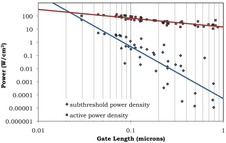
1.1. The increase in the subthreshold and active power density with gate length scaling is shown. The increase in the passive power density is seen to be approaching that due to the active power density and shall surpass the active power density at the
Gordian knot.
3
1.2. Spin as another dimension which may be manipulated independent of the electric field, allowing for greater functionality within the same physical space.
4
1.3. Emerging devices envisioned for solutions beyond CMOS reported in the ITRS 2007.
5
1.4. The evolution of the MTJ stack over the years. 9
1.5. The transmission of electrons when the free layer magnetization is parallel (a) and anti-‐parallel (b) to the fixed layer.
11
1.6. A schematic representation of the device structure of the MTJ 12
1.7. The mask layout and cross-‐sectional diagram of the MTJ stack 15
1.8. Three different MTJ lots developed in the first attempt at fabricating the devices. Notice that the first devices used Al2O3 as the tunneling barriers. Note that the
above graphs are reproduced from Stephen’s thesis. The thicknesses of the bottom electrodes are actually incorrect. There is a 200nm thick Al layer that acts as the
xv
bottom electrode, on top of which the rest of the stack is located.
2.1. A chart showing the list of analytical techniques employed in this study. 21
2.2. A schematic representation of the method used for four-‐point measurement (a) and the layout of the structure for doing the same (b)
24
2.3 A schematic representation of the test setup used for measuring the TMR of the MTJs.
25
2.4. The interactions between a sample and an electron beam 23
2.5. relationship between the wavelength of an electron, and its acceleration voltage. 27
2.6. A sample sliced into a thin layer for TEM measurements using a FIB (a), a bright field image of the sample (b) and a dark field image of the sample (c).
28
2.7. Optical ray diagrams for forming bright-‐field (a), dark-‐field (b), and high-‐ resolution images (c) in a TEM.
29
2.8. HRTEM Images of a CoFe grain sandwiched in between an MgO grain. 30
2.9. Basic principle of Electron Energy Loss Spectroscopy (EELS). 31
2.10 The x-‐ray diffraction pattern due to a single-‐crystal sample (a) and that due to a poly-‐crystalline sample (b) is shown.
32
2.11 A picture of the sample stage mounted on an eulerian cradle (a), the whole XRD set-‐up (b), and a schematic representation, representing the various parts of the system (c).
xvi
3.1. A schematic representation of a tunneling-‐barrier grown on top of a rough bottom-‐ electrode. The fig. is not to scale. The direction of magnetization of the pinned layer is shown by red arrows while that of the free layer is shown by blue arrows.
38
3.2. A shift in the B-‐H curve is shown due to magnetic coupling between the free layer and the upper pinned layer resulting from surface roughness.
38
3.3. Oscillations in antiferromagnetic coupling as a function of Ru thickness is shown above.
39
3.4. A schematic representation of the advantage of using a non-‐magnetic spacer layer is shown.
40
3.5. A comparison of the interfaces formed between AlOx (a), as-‐deposited MgO (b) and MgO after being annealed at 375ºC (c). Notice that the AlOx forms an
amorphous layer while MgO forms a crystalline layer. The interface quality between MgO and CoFeB increases significantly after the MTJ stack is annealed.
43
3.6. The updated stack used for Phase II of the fabrication process 45
3.7. The MTJ patterning technique using a photoresist mask. 47
3.8. Crystalline characteristics of different materials before and after in-‐situ annealing. Ta peaks are clearly visible before annealing (a), an MgO peak is observed only after annealing at 400°C for 1 hour (b) and no significant differences are observed for unannealed NiFeCr and Ru before anneal (c) and after a 350°C anneal (d) and similarly, no change in Ru crystallinity before (e) and after anneal (f).
xvii
3.9. A TEM cross-‐section with PEELS analysis depicting the different layers along with a schematic representation of the layered structure that I intended to be put down. Note that the schematic isn’t to scale, and the numbers in brackets are thicknesses in nm of layers that are intended to be deposited.
54
3.10. The TEM micrograph of the device structure showing the bottom electrode, the seed layer, the MTJ layer, the Ru capping layer and the top electrode (a), and a zoomed-‐in section (b) showing the details of the MTJ stack.
55
4.1. The as-‐deposited samples used for studying the effects of anneal on different layers of the MTJ. The study of the interaction of CoFeB and MgO only is studied in (a), while the interaction of CoFeB, MgO and Ru is studied using the sample shown in (b).
59
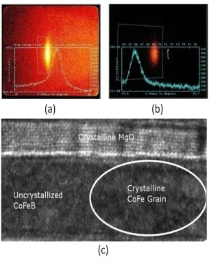
4.2. XRD images obtained for the MgO (200) peak (a) and a CoFe (200) peak (b) are shown. A grain of crystalline CoFe is seen surrounded by uncrystallized CoFeB at the CoFeB|MgO interface in (c).
62
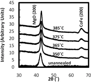
4.3. Relative XRD Intensities as a function of 2θ is plotted with the anneal temperature as a parameter, showing the MgO (200) and the CoFe (200) peak. The data is extracted from 2D-‐measurements similar to those shown in Fig. 4.2.
63
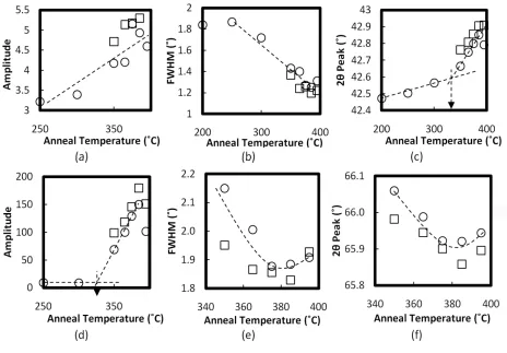
4.4. Characteristics of Gaussian data fits (represented by amplitude, FWHM and the 2θ peak position) are plotted as a function of anneal temperature, for the MgO (200) peaks (a),(b) and (c) and for the CoFe (200) peaks (d),(e) and (f).
64
4.5. The (200) lattice parameter for MgO (squares) and CoFe (circles) are plotted as a function of anneal temperature is plotted in (a). The percentage mismatch
xviii
between the CoFe lattice and the MgO lattice as a function of temperature is shown in (b).
4.6. The crystal size of individual grains of CoFe (circles) and MgO (squares), as well as the contact area ratio of the individual crystals (crosses) as a function of
temperature are shown in (a). A schematic representation (not to scale) of individual grains of CoFe on top of an MgO grain is shown in (b).
68
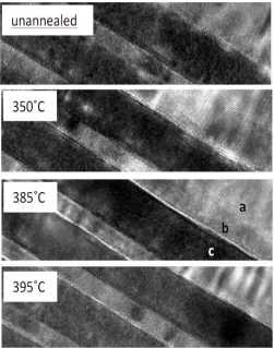
4.7. TEM images of the unannealed sample, and those annealed at different
temperatures is shown. As may be observed from the TEM images, interfaces are steadily improved with anneal temperatures. Lables ‘a’, ‘b’ and ‘c’ are physical locations for the PEELS line-‐scans shown in Fig. 8.
70
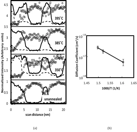
4.8. B K edge (a) and O K edge (b) at a location deep inside the MgO capping layer (open squares), near the interface (solid line) and inside the CoFeB layer (open circles) for the sample annealed at 395 °C.
71
4.9. The variation in the normalized intensity of the oxygen peak around 536 eV (solid line), the gap state energy loss at 530 eV (dashed lines), and for boron around 193 eV (open squares) and 230 eV (open circles), as a function of PEELS scan distance (a), and plot of boron doffusion coefficient in MgO as a function of temperature (b).
73
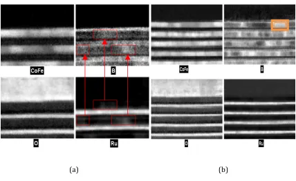
4.10. The presence of different elemental compositional analysis as a function of the position in the sample, for samples annealed at 500°C (a), and for samples
annealed at 395°C (b). Note that a white spot indicates the presence of a particular chemical species.
xix
5.1. Material Stacks designed for finding the variation of the TMR for different
configurations. The thickness of the MgO is varied in (a) for finding the variation of TMR and the parallel and antiparallel resistances as a function of MgO thickness. In (b), an antiferromagnetic layer is used to see if the lower pinned layer can be atomically coupled to the permanent antiferromagnetic stack.
76
5.2. The MTJ patterning technique using a Ta hardmask. 77
5.3. The structural integrity of post-‐deposited samples with a 1nm thick layer MgO (a) and 2nm thick MgO layer (b) by design is shown.
78
5.4. Magnetization curves obtained for three different samples before annealing, and after annealing at 380°C for one hour.
80
5.5. The AMR measurement for the sample shown on Fig. 5.3.(a) showing a definite change in resistance as the magnetization is changed.
81
5.6. The background SIMS traces obtained during the ion-‐milling of wafers containing layers similar to that shown in Fig. 5.3.(a), and of wafers containing layers similar to that shown in Fig. 5.3.(b) (b) are shown.
83
5.7. 3D AFM images of the side-‐walls of some of the fabricated MTJ’s 85
5.8. The SEM image of a 3µm×3µm MTJ MESA (a), with a corner zoomed out to see the damage due to the ion-‐milling (b), and that of a larger 9µm×9µm MTJ MESA, showing an intact MESA with what appears to be re-‐deposition at the edges.
86
xx
bottom electrode is indeed present.
5.10. A schematic representation of measuring the I-‐V characteristics of the MTJ MESA using an AFM
88
5.11. The CAFM measurements of a 3µm×3µm MTJ device. 89
6.1. A TEM image of a CoFe grain embedded in a CoFeB matrix (a), and a schematic representation of the same (b).
89
6.2. Three square grains at a distance of r away from each other (a), and the possible positions of such grains when these grains are removed a distance nr away (b).
102
6.3. Plots of the value if P, the probability of finding a CoFe grain at a particular point (x,y) for different parameters.
103
6.4. A schematic representation of a unit BCC structure, showing the direction-‐cosines of the central atom to a nearest atom, and one of the next-‐nearest atoms.
104
6.5. Fits (lines) to the dispersion relationships calculated using first principles (symbols) for majority spin bands (a), and minority spin bands(b).
111
6.6. Fermi surfaces for the majority spin bands (a) and the minority-‐spin bands (b) 114
6.7 Fermi velocities superimposed upon the Fermi surface, showing the distribution of the velocities about the Fermi surface.
116
6.8. In (a), an electron originating from one side of the rectangular barrier exits the barrier on the other side at point P1, and in (b), a distribution of these points for all
electrons having a Fermi surface resembling one shown in Fig. 6.7.
xxi
6.9. Schematic representation of a Fermi sphere representing an electron in an isotropic medium.
119
6.10. The distribution of electrons originating at the origin on one side of the barrier from a Fermi sphere, on the other side of the barrier.
122
6. 11. The probability of finding a CoFe grain with tGrain = 1×10-20t(a), 6t (b), 12t (c),
and 18t (d).
124
6.12. The TMR’s as a function of barrier thickness, with tGrain as a parameter. The values of the probability function used are shown in the previous figure.
126
6.13. The variation of TMR as a function of the grain size. 127
7.1. The main components of the MTJ macro-‐model is shown. It is broken down into three major sub-‐circuits – the MTJ magnetic sub-‐circuit which implements specifics of the input hysteresis or the asteroid curve (as the case may be,) the bi-‐ stable memory element which is useful for saving the relative orientation of the free-‐layer, and finally the MTJ electrical sub-‐circuit which models the voltage dependence of the resistances in the parallel and anti-‐parallel states
128
7.2. A schematic representation of the process of representing a voltage-‐dependent nonlinear resistor using elements of SPICE Version 2G is shown. First the nonlinear resistor function f(V) is mapped into a convenient representation comprising of a linear resistor and a nonlinear resistance function (a), and then the newly mapped non-‐linear resistance function is represented by a dependent current source which draws the same amount of current which would have flowed
xxii
through resistance R2 (b).
7.3. Representitive I-‐V curves one of which does not converge (Curve I), and the other which does converge (Curve II) during a Newton-‐Raphson iteration in a simulator.
137
7.4. A schematic representation of the sub-‐circuit used for representing the nonlinear voltage dependence of the MTJ in.
137
7.5. Measured R-‐V characteristics from compared to SPICE simulations. The solid lines represent the measured high and low resistances in the anti-‐parallel and parallel configurations separately. The open circles represent the SPICE simulation for the
Rap sub-‐circuit and the open squares represent the SPICE simulation results for the
Rp sub-‐circuit.
139
7.6. The implementation of the voltage controlled switch is shown. The control voltage Vsc is used to switch between a high or a low voltage, which in turn is converted by a VCCS to a conductance proportional to the input voltage.
140
7.7. Implementation of the bi-‐stable memory element is represented schematically above. An ideal OPAMP with a differential gain of 1000, a single pole having a time constant of 1ns, a 1mA current limiter and a ±5V voltage limiter (a) is used in a regenerative feedback loop (b) forming a Schmitt trigger. An input buffer with associated voltage limiters isolates the trigger from variations in impedances of the input circuitry, while a voltage shaping circuit and another isolation circuitry isolates the trigger from variations in the output impedances.
141
7.8. Simulations of the transfer characteristics of the Schmitt trigger of Fig. 7.6 without the use of a voltage shaping circuit in comparison to the output characteristics in
xxiii
the presence of the voltage shaping circuit are shown in (a). Notice the constant bi-‐ stable output voltages with the proper pulse shaping circuit. A transient
simulation of the internal node voltages are shown in (b). The y-‐axes in (b) have units of volts.
7.9. An implementation of the Magnetic Sub-circuit comprising of only one input current. The write current is applied via the external terminals marked 1 and 2, while the output voltage is obtainable through the external node marked 3.
145
7.10. The simulations of the transfer characteristics of the magnetic sub-‐circuit
connected to the Schmitt trigger is shown above. It is overlaid with the hysteresis measured due to the device.
146
7.11. A sub-‐circuit comprising of three MTJs forming a very basic flash converter. Set currents may be used at any time to change the resistances, thus changing the behavior of the comparator dynamically.
148
7.12. Transient simulation results of the circuit shown in Fig. 9 is shown above. The set-‐ currents (a) are used to set an initial state of the MTJs during the first part of the simulation, and then they are used again, in the second half of the simulation to set the MTJs to a different state. The resulting electrical simulations (b) show output characteristics which are similar in form but numerically different during the two measurement intervals.
149
II-1. The design space of the experiment, with the variable parameters of the deposition conditions shown as circles within the design space.
xxiv
II-2. The process of flattening a raw image (a) to remove contributions due to the tilting of the sample during the measurement process to obtain a
normalized image (b) on which proper measurements may be
performed. The process of obtaining statistical measurements from the
sample shown in (b) comprises of dividing up the heights of each of the
pixels in the images into a hundred separate distributions and then
obtaining statistical measurements of the heights from them is shown
in (c).
159
II-3. The RBS result for the formation of NiCr after sputtering from an Ni:Cr::80:20 target. As can be seen, the Ni:Cr::77:23 ratio is consistent
with the target concentration.
160
II-4. The process of finding the size of the grains from a raw image (a). A cross-section taken along a particular direction (a) reveals a number of
peaks and valleys (b) representative of the grains. For avoiding
measurement errors resulting from the directionality of the
measurements, five separate directions are chosen as shown in (c) and
their results averaged over to obtain a final value of the grain size.
161
II-5. The raw AFM images for different sputtering conditions is shown. The variation of the surface properties on the sputtering conditions is
immediately apparent.
162
II-6. The dependence of the RMS surface roughness on the sputtering conditions showing an almost linear dependence of the roughness over
the input parameter space (a), and the relationship between the grain
xxv size and the RMS roughness is shown in (b).
II-7. 3D AFM images of the surface properties of the sample with the best
surface properties (a) and the worst surface properties (b) is shown.
164
II-8. The dependence of the sheet resistance, the thickness and the bulk
resistivity of NiCr films on the RMS roughness to investigate and
correlation between the surface roughness and the resistive nature of
the material at room temperature.
165
III-1. The Bruce 2 furnace recipe developed for annealing the wafers. 166
III-2. The Si-O absorption characteristics for FTIR measurements obtained
after curing the ILD at 250°C (a) compares favorably with sample
characteristics obtained from Honeywell (b).
1
1. INTRODUCTION
Brisk developments in information technology, and the proliferation of devices with the
ability to capture an ever-increasing plethora of audio, video, and various other sensory
information in digital form has created a huge demand for fast and reliable ways of storing,
retrieving and processing information. Improvements in speed and capacity have thus far been
achieved via the scaling of devices. However, physical scaling appears to garner greater
hindrance, as the device sizes approach atomic scales. For augmenting physical scaling, other
natural degrees of freedom, such as spin are being currently explored. The commercialization of
such devices in the form of high-density hard-drive read-write heads have catalyzed much rigor
in spintronics research, culminating in the 2007 Nobel prize in physics.
1.1. Current Trends in Scaling
Scaling in the semiconductor electronics industry generally refers to the shrinking of device
dimensions with the progression of the years, characterized by what is ubiquitously known as
Moors Law [1]. This is not exactly a physical law, but the combined effort of a group of
motivated individuals to obtain more functionality and faster performance in the same electronic
equipment, cheaper than ever before. All this, by simply reducing the dimensions of the simplest
building block of the electronic circuits: the transistor. However, scaling has not always been an
easy, and is getting ever more difficult now as some of the critical dimensions (such as gate
thicknesses) are approaching atomic dimensions. Some of the biggest problems that are facing
the industry are described below. Then, a new dimension it electronics is presented, something
that has become practicable only in recent years. This dimension has the potential of advancing
2
1.1.1. The Power Wall
One of the greatest adversaries to scaling has been a point on a power-‐gate length graph known as the Gordian knot [2], shown in Fig. 1.1 as the point of intersection between the red and the blue lines. The red line represents the increase in the active power per square centimeter of the chip, as the dimensions of MOS transistors decrease. However, the blue line represents power per square centimeter of the chip when the transistor is in the off state, i.e. when the transistors are not supposed to not pass current through them. Some current does pass through, however, and has a logarithmic dependence upon the threshold voltage VT, given by
I
OFF∝
exp
(
−
V
Te
/
nkT
)
, (1.1)Where IOFF is the off-‐state current represented by the k is the Boltzmann constant, T is the
absolute temperature and e is the electronic charge. N is approximately 1.4 for practical design. Since, VT scales with the voltage across the device VDD which in turn scales with gate length. The
ration of off-‐state power to the on-‐state power is a good indicator of the inefficiency of the chip. The knot shown in the figure represents the point where the off-‐state power shall overtake the on-‐state power, and represents the point where the inefficiency of the system will become a significant. The only way of augmenting the inefficiency would either be to find new devices, or new materials to make the devices, or to turn off the power altogether.
There have been significant strides toward materials research, novel device technologies, multiple VT, VDD, LGATE and TOX offered for the same technology node and on the same wafer, and
3
Fig. 1.1. The increase in the subthreshold and active power density with gate length scaling is shown. The increase in the passive power density is seen to be approaching that due to the active power density and shall surpass the active power density at the Gordian knot.
1.1.2. Spin as Another Dimension
The electrons have only but a few fundamental properties – their mass, electric charge and spin. Current electronics employs the charge of the electrons to impart momentum to them using electric fields, by letting them fall down electric potentials. However, the spin of the electrons has been largely ignored – until recently. Today it is possible to manipulate the electric charge and the spin simultaneously. Thus, not only is it possible to affect the movement of electrons using the charge of the electrons, but also the spin of the electrons. This allows some very remarkable possibilities, a small survey of which shall be provided in the next chapter. However, it is interesting to note that this inclusion of the spin of the electron would allow for the manipulation of the electron in another
0.000001 0.00001 0.0001 0.001 0.01 0.1 1 10 100
0.01 0.1 1
P
o
w
er
(W
/
cm
2)
Gate Length (microns)
[image:29.612.95.479.111.354.2]4
parameter space, or an additional dimension. Thus, the electron is able to translate in both an electric potential and in the magnetic potential, as shown in Fig. 1.2.
Fig. 1.2. Spin as another dimension which may be manipulated independent of the electric field, allowing for greater functionality within the same physical space.
The momentum of the electrons (represented by p) is governed by both the electric field (E) and the magnetic field (H). This, however is not the end of the story. Since the presence of an electric field depends upon the reference frame of the observer, depending upon the path of the electron, the electron might see the local electric potential as a magnetic potential. Several devices have been reported utilizing this effect. Further, these spin-‐polarized electrons may also be used as a stepping-‐stone for accessing the nuclear spin in certain materials and that will possibly allow one to realize quantum computers.
Spin-‐based devices are being considered for increasing the density of existing devices in the International Technology Roadmap (ITRS) 2007.
E
H
p
5
Fig. 1.3. Emerging devices envisioned for solutions beyond CMOS reported in the ITRS 2007.
1.2. Spin Phenomena in Different Material Systems
6
The idea of using spin for electronic computation had already been proposed by such visionaries as Feynman [4] and Landauer [5]. Recently, magnetic [6] and ferromagnetic [7] semiconductors are used for the injection of spin polarized electrons into semiconductors and that these electrons have long diffusion lengths (in GaAs for example [8]).
Magnetic metals have been widely studied, and are the primary material of choice for the MTJ. The phenomenon of spin transport in such material systems is obviously very important and pertinent to the present study. Thus a whole section has been devoted to the phenomenon of transport in magnetic metals, and shall be discussed later in much greater detail. This section provides an overview of the major transport phenomenon in other material systems and their potential applications.
Nonmagnetic metals do not generally have identical densities for both the spin-‐up and spin-‐ down states around the Fermi level. There is however, a Spin Hall effect, due to which electrons of opposite spin polarity flow along opposite ends of the wire, in opposite directions[9, 10]. This effect has been shown in Al [11] (and the magnitude of the effect corresponds closely with predicted values [12, 13]) and ZnSe [14]. The spin Hall effect has potential applications in routing packets of spin for routing or logic. Another interesting property of nonmagnetic metals is that most of these materials have strong spin-‐orbit coupling. In the absence of a magnetic field, strong momentum-‐ scattering occurs due to the spin-‐degeneracy of the metals, with lifetimes as low as a few femtoseconds. During this process, there is a strong propensity for a spin-‐flip process as well. This is known as the Elloitt-‐Yafet [15, 16] process. It has been observed in Cu [17] and may be used as spin-‐relaxers.
7
these rare-‐earth magnetic insulators are not magnetically ordered at room temperatures. Magnetic semiconductors have been proposed by hosting magnetic dopants in nonmagnetic semiconductors such as In1-xMnxAs and Ga1-xMnxAs to have similar characteristics[21-‐23]. When the density of the
dopant Mn atoms becomes high enough, through the double-‐exchange mechanism[24, 25], parallel orientation of holes results in substantial reduction in energy, which in turn drives the ferromagnetic state. The importance of holes mediating the ferromagnetic state immediately makes them significantly more important than their insulator counterparts, since it is possible to control the hole concentration using some gating mechanism. Both the Curie temperature [26] and the coercive field [27] has been successfully changed using such a technique. Unfortunately, the rather high doping levels of Mn, their relatively low fabrication temperatures and their low (i.e. lower than room-‐temperature) Curie temperatures have rendered them very difficult to fabricate. Nevertheless, simple device have been demonstrated [28].
8
structure of the effective magnetic field, which in turn depends upon the inversion symmetry of the material. Control of the spin polarization by the control of inversion symmetry, either by growth [30-‐32], or by an applied electric field [33] (also known as the Rashba field) has been demonstrated.
1.2.1. Applications in Memory and Logic
Spin states of electrons have already been used for making memory devices. The MRAM developed at Freescale [34] and IBM [35] and the racetrack memory developed at IBM [36, 37] bears testimony to that. In the past however, the spin of the electrons have been used for memory for a long time in magnetic hard-‐drives. During the early days, of course, hard-‐drives were not thought of as spin devices, but rather magnetic devices. It was only after the introduction of the GMR read-‐write heads by IBM for their hard-‐disk drives that spintronics gained some momentum. Other than GMR read-‐write heads, magnetic sensors [38] had been devised based on the spin-‐valve.
Other than these commercial devices, several different types of transistors, including SpinFETS [39-‐41], magnetic bipolar transistors [42, 43] and hot electron transistors [44, 45] have been proposed or demonstrated. Spins in single electron transistors have also been studied [46] for the purpose of realizing the quantum computer [47]. Some circuits and devices have also been proposed for reconfigurable logic [48], multiple valued logic [49, 50] and CAM-‐based logic architectures [51-‐53], which has immense ramifications for future electronic systems.
1.3. Magnetic Tunnel Junctions
9
1.3.1. Introduction to Magnetic Tunnel Junctions
The MTJ comprises of two ferromagnetic electrodes separated from one another by a tunneling barrier. These ferromagnetic electrodes are generally patterned into micro-‐ and nano-‐scaled devices, whence the natural tendency of the electrodes is to from a single-‐domain structure. These, either using shape-‐ or natural-‐anisotropy are made to magnetize either in the parallel or antiparallel directions, depending upon whether the magnetizations of the two layers point in the same direction or in the opposite directions, respectively. When the magnetizations of the two layers are parallel, the overall resistance of the overall structure of the three layers is less, than when the magnetizations of the two layers are antiparallel. The possibility of discrimination of the two resistive states at room temperature is what is used as memory. Since ferromagnetic layers allow for the retention of the magnetic information without the expenditure of external energy, nonvolatile operation is possible. The basic MTJ stack is shown in Fig. 1.4(a) which was what was used for most of the experimental investigation of the TMR phenomenon.
However, due mainly to the work of S. S. S. Parkin and others, significant progress
has been made to the basic structure of the MTJ so as to make it more suitable as for
the commercial applications.
Fig. 1.4. The evolution of the MTJ stack over the years [35].
Insulating Barrier
Free layer Fixed Layer SAF Coupling
Layer Lower fixed layer Antiferro-magnetic layer
10
The first advancement was the introduction of the SAF stack that replaced the
fixed layer. This resulted in removing any stray magnetic field that would emanate
from the lower pinned layer. This was also a major improvement since, the SAF layer
could be engineered to have just enough residual magnetism so as to overcome the
effect of Neel coupling which was always present in initial iterations of the stacks.
Simultaneously, another scheme was introduced which allowed for the pinning to take
place at the atomic level. This involved the use of a natural antiferromagnetic layer
which, once annealed, would result in the formation of a very strong atomic coupling
of the magnetic field, and would itself resist demagnetization in magnetic fields, since
as a whole, the antiferromagnetic layer did not have an intrinsic magnetic field. Soon
afterward, the antiferroamgnetic layer was coupled with the idea of the SAF stack to
give the structure that is most prevalent in the industry today. Of course, there have
been some changes simple changes such as the design of structures having a natural
anisotropy in the magnetization, or the use of an SAF stack in the lower as well as the
upper pinned layer, but the overall structure and stack has been what is shown in Fig.
1.4.
11
1.3.2. MgO as a Tummeling Barrier
Several authors [54, 55] did several studies on the first principles studies on the transport properties of electrons through a thin layer of MgO when sandwiched between ferromagnetic electrodes. MgO being crystalline had a well-‐defined dispersion relationship. The
Δ
1 spd orbitalpresented a path for the electrons conducting via electrodes polarized parallel to each other, and thus decay at a much slower rate. Further, another pd orbital presents an orbital which provides a similar path for the conduction of such electrons wish a slightly greater rate of decay of the evanescent waves. The majority transmission probability of the parallel configuration has a peak near the k||=0 direction is significantly greater for the parallel configuration than that of the
antiparallel configuration.
(a) (b)
Fig. 1.5. The transmission of electrons when the free layer magnetization is parallel (a) and anti-‐parallel (b) to the fixed layer.
12
interfaces such as the Co|Al2O3|Co [56], Co|MgO|Co [57], FeCo|MgO|FeCo [58], and the formation of
interfacial structures between MgO and Fe [59] have similarly been explored. Following the discovery of MgO, several research groups immediately ventured to take advantage of the new material, with significant success.
1.3.3. Device Structure
A schematic representation of the device structure commonly used at present times is shown in Fig. 1.6.
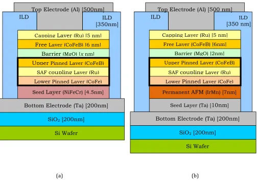
Fig. 1.6. A schematic representation of the device structure of the MTJ.
Significant details about each of the layers are provided in Chapter 3. However, a brief description of the layers is present here. The lowest layer is the Si wafer, on top of which a oxide is grown. This is a insulating layer upon which the MTJ structure is going to be built. Also, as an aside, this is also the layer upon which lithographic patterns are etched, so that other levels might be aligned to one another. The MTJ being a two-‐terminal device, is probed from one side by the bottom
Bottom Electrode (NiCr or Ta) [200nm]
Lower Pinned Layer (CoFe) [1.1nm] Barrier (MgO) [1nm]
Free Layer (CoFeB) [2nm] Capping Layer (Ru) [7nm]
Top Electrode (Al) [500nm]
SAF coupling Layer (Ru) [0.85nm] Upper Pinned Layer (CoFeB) [2nm]
ILD [350nm] ILD
SiO2 [200nm]
13
layer, and from the other by the top electrode. The layers between the top and the bottom electrode comprises of the MTJ layers. The top MTJ layer is a capping layer, and is used for protecting the MTJ from oxidation and structural damage during processing. The next layer from the top (CoFeB) is one of the ferromagnetic electrodes, that sits on top of the MgO barrier. This is the free layer and is switched during the ‘write’ process. The stack of three layers that support the MgO barrier together compose of the other ferromagnetic electrode. This is called the synthetic antiferromagnetic stack. These three together combine to form a robust synthetic antiferromagnet, with little stray magnetic field, and significant saturation magnetization, and as such is immune to low external magnetic field. An inter-‐level dielectric separates the top and the bottom electrodes.
1.3.4. Applications
MTJ’s are primarily used commercially in read/write heads of hard-‐disks. This single invention is the primary reason for the significant increase in the storage capacities of the hard-‐disks. These have recently attracted great attention as non-‐volatile storage elements. These have also been used as magnetic sensors, and have been proposed to be used for reconfigurable computing.
1.4. Integration with Silicon at RIT
Upon integration with Si, the MTJ leads to useful applications in random access memory, sensors and may be used for reconfigurable logic applications. Yemura et al. [60] proposed a novel concept of four-‐valued MRAM. Sudirgo [61] attempted to integrate the MTJ device shown in section 1.4.1 with silicon-‐based resonant interband tunneling diode (RITD). A brief review of the processing challenges encountered by Sudirgo are described below.
1.4.1. Device Fabrication – Phase I
14
section. After the first attempt, several changes were made in the fabrication process. Another attempt was made at fabricating the devices, described in Chapter 3, after ameliorating the process. In this attempt, severe interdiffusion of the different layers was observed. For understanding the reasons behind this interdiffusion, detailed materials analysis was performed. The materials analysis is described in detail in Chapter 4. Finally, the updated fabrication process is described in Chapter 5.
1.4.1.1. Design
Several test structures were designed for the implementation of the MTJ on a Si platform. These comprised of TLM structures, cross-‐bridge structures for measuring resistances and contact resistances between various layers, and structures for four-‐point probe measurement. An overview of the mask layout for the four-‐point probe measurement, and the principle behind its operation has been described in the Chapter 3. In Fig. 1.7, a more detailed explanation of the current conduction process is shown.
15
The section of the MTJ within the layout is zoomed out to reveal the details of the layout. Charge enters the MTJ, from the terminal 1, travels through ‘Metal 1’ until it reaches the MTJ. It then travels through the MTJ, and out of terminal 4, via the bottom electrode The voltage is measured between terminals 2 and 3, which connect to both ‘Metal 1’ and the ‘Bottom Electrode’. The fabrication of this device is described next.
Three stacks were designed for the MTJ. These are shown in Fig. 1.8.
(a) (b) (c)
Fig. 1.8. Three different MTJ lots developed in the first attempt at fabricating the devices. Notice that the first devices used Al2O3 as the tunneling barriers[61]. Note that the above graphs are
reproduced from Sudirgo’s thesis. The thicknesses of the bottom electrodes are actually incorrect. There is a 200 nm thick Al layer that acts as the bottom electrode, on top of which the rest of the stack is located.
1.4.1.2. Processing: Phase I
16
1. 500 nm of thermal oxide was grown on a Si wafer, 2. 200 nm of Al was deposited as the bottom electrode, 3. MTJ stacks were deposited,
4. The MTJs were field-‐annealed,
5. MTJ Mesas are defined using photoresist,
6. A MESA etch is performed, which stops at the bottom electrode, 7. The photoresist is stripped using a standard O2 plasma asher,
8. The bottom electrode is patterned using photoresist, 9. Al wet etch is used for the etching of the bottom electrode, 10. The photoresist is stripped using a standard O2 plasma etcher,
11.300 nm of PECVD TEOS is grown, 12.Contact cut is defined,
13.Contact cuts are etched using HF/dry CHF3,
14.The photoresist is stripped using a standard O2 plasma etcher,
15.200 nm of Al is deposited during using sputtering, 16.Metal 1 definiiton,
17.Metal Etch using the Al wet etch, and
18.The photoresist is stripped using a standard O2 plasma etcher.
1.4.1.3. Results
17
Proposed solutions for these shall be presented in Chapter 3.
TABLE 1.1.
Problems in fabrication encountered during the first attempt at fabricating the MTJ Problem Proposed Workaround for Phase II
The bottom electrode is patterned after the MESA etch. During ion-‐milling, the bottom electrode is etched away.
The bottom electrode is first patterned, and then the MESA is etched using ion-‐milling. The material of the bottom-