Scattering in Graphene
.
White Rose Research Online URL for this paper:
http://eprints.whiterose.ac.uk/89594/
Version: Published Version
Article:
Ferreira, Aires orcid.org/0000-0001-6017-8669, Rappoport, Tatiana G., Cazalilla, Miguel A.
et al. (1 more author) (2014) Extrinsic Spin Hall Effect Induced by Resonant Skew
Scattering in Graphene. Physical Review Letters. 066601. ISSN 1079-7114
https://doi.org/10.1103/PhysRevLett.112.066601
[email protected] https://eprints.whiterose.ac.uk/ Reuse
Items deposited in White Rose Research Online are protected by copyright, with all rights reserved unless indicated otherwise. They may be downloaded and/or printed for private study, or other acts as permitted by national copyright laws. The publisher or other rights holders may allow further reproduction and re-use of the full text version. This is indicated by the licence information on the White Rose Research Online record for the item.
Takedown
If you consider content in White Rose Research Online to be in breach of UK law, please notify us by
Extrinsic Spin Hall Effect Induced by Resonant Skew Scattering in Graphene
Aires Ferreira,1Tatiana G. Rappoport,2Miguel A. Cazalilla,3,1 and A. H. Castro Neto1,4
1
Graphene Research Centre and Department of Physics, National University of Singapore, 2 Science Drive 3, Singapore 117546, Singapore
2
Instituto de Física, Universidade Federal do Rio de Janeiro, CP 68.528, 21941-972 Rio de Janeiro, RJ, Brazil 3
Department of Physics, National Tsing Hua University, and National Center for Theoretical Sciences (NCTS), Hsinchu City, Taiwan
4
Department of Physics, Boston University, 590 Commonwealth Avenue, Boston, Massachusetts 02215, USA
(Received 8 May 2013; published 11 February 2014)
We show that the extrinsic spin Hall effect can be engineered in monolayer graphene by decoration with small doses of adatoms, molecules, or nanoparticles originating local spin-orbit perturbations. The analysis of the single impurity scattering problem shows that intrinsic and Rashba spin-orbit local couplings enhance the spin Hall effect via skew scattering of charge carriers in the resonant regime. The solution of the transport equations for a random ensemble of spin-orbit impurities reveals that giant spin Hall currents are within the reach of the current state of the art in device fabrication. The spin Hall effect is robust with respect to thermal fluctuations and disorder averaging.
DOI:10.1103/PhysRevLett.112.066601 PACS numbers: 72.80.Vp, 72.25.-b, 73.20.Hb, 75.30.Hx
The spin Hall effect (SHE)[1–4], that is, the appearance of a transverse spin current in a nonmagnetic conductor by pure electrical control, has been predicted to occur in materials with large spin-orbit coupling (SOC). Over the last decade, its study has lead to an intense experimental activity[5–9], due to its potential application in spintronics. Recently, the SHE has been explored for replacing ferro-magnetic metals with spin injectors in applications
[10,11], opening the door to the development of spintronic devices without magnetic components.
The activation and control of spin-polarized currents is both of fundamental and technological interest. The SHE could be used for an efficient conversion of charge current into spin-polarized currents. The ratio of the spin Hall current to the steady-state charge current, commonly known as the spin Hall angleθsH, measures this efficiency and it is the most important figure of merit for practical applications. Generally speaking, the SHE in metals and semiconductors originates from (i) extrinsic mechanisms, which are due to spin-dependent scattering of charge carriers by impurities in the presence of SOC [1–3], and (ii) intrinsic mechanisms, entirely due to SOC in the electronic band structure, which occur in the absence of any scattering process. In semi-conductors, the spin Hall angles are in the range of 0.0001– 0.001 [5,7]. On the other hand, θsH for metals can be considerably larger, being of the order of 0.01 for Pt[12]
and 0.1 in a recent measurement performed in Ta[11]. Since its successful isolation, graphene [13] has also become the subject of intensive study in spintronics
[14–18]. In this material, electrons can propagate ballis-tically and the carrier density and polarity can be controlled by an external gate. Spin-orbit and hyperfine interactions are extremely weak in graphene and therefore the spin coherence length is expected to be long [19,20]. These
characteristics make graphene appealing for passive tronic applications, e.g., as a high-fidelity channel for spin-encoded information [21]. A striking possibility is to modify graphene for active spintronics. This may be achieved via spin-orbit splitting of the band dispersion, e.g., by bringing heavy metallic atoms in close contact to graphene [22], or by locally inducing sizeable SOC (∼10meV) [23,24]. In Ref.[23], distortions induced by covalently bonded impurities were predicted to produce the desired effect, and Ref.[24]suggests local SOC enhance-ment via tunneling of electrons in and out of a heavy atom. Phenomenologically, random spin-orbit fields have also been predicted to generate a nonzeroθsH[25]. Moreover, it has been proposed that, in the presence of SOC, graphene could exhibit the quantum spin Hall effect[26].
promising candidate for spintronic integrated circuits with SHE-based spin-polarized current activation and control.
According to our calculations, the extrinsic spin Hall effect in graphene, as that recently reported in hydro-genated graphene samples[32], can originate from skew scattering alone. The latter is absent in the first Born approximation[33] and, therefore, we compute transport relaxation rates nonperturbatively via exact partial-wave expansions. Our results indicate that functionalized gra-phene can deliver spin Hall angles comparable to those found in pure metals (θsH∼0.01–0.1[5,7,12]).
In order to investigate the extrinsic SHE and its depend-ence on Fermi energy and temperature, we consider a continuum model of graphene decorated with a small concentration of impurities that locally generate SOC over nanometer-size regions. The latter could be metallic nano-particles inducing SOC via the proximity effect, but other physical realizations are also possible. (In fact, adatoms in graphene often cluster due to ripples[34]or due to a low adsorption energy[35].)
Our starting point is the continuum-limit Hamiltonian of graphene H0¼ℏv
FðτzσxpxþσypyÞ, wherep¼ ðpx; pyÞ
is the 2D kinematic momentum operator around one of the two inequivalent Dirac pointsKandK0,vF≈106 m=s
is the Fermi velocity, andσ and τ denote Pauli matrices, with σz¼ %1 [τz¼ %1] describing states on the AðBÞ sublattice [atKðK0Þ]. The spin-orbit splitting in the band
structure of pristine graphene is of the order of10μeV and therefore can be safely neglected[20]. The large scatterers considered here induce sizeable local SOC of the intrinsic-type VðSOIÞ¼Δ
IðrÞτzσzsz and/or Rashba-type V
ðRÞ SO ¼
Δ
RðrÞðτzσxsy−σysxÞ; here, s are Pauli matrices for spin
andr¼ ðx; yÞis the charge carrier position. The
depend-ence ofVðSOIÞin the spin and orbital operators is the same as the SOC in flat, pristine graphene. On the other hand,VðSORÞ
originates in perturbations breaking mirror symmetry about the graphene’s plane (e.g., single-site adsorption). The impurity potentials are assumed to be smooth on the lattice scale and thus sublattice symmetry breaking terms (crucial in the single adatom limit[36]) are not considered here. For such large scatterers intervalley scattering is negligible and, in the long wavelength limit, assuming that potentials have radial symmetry, the scatterer is described by
VadðrÞ ¼VSOðrÞ þV0ðrÞ; (1)
where r¼jrj, and the (spin-independent) electrostatic potential V0ðrÞ accounts for extra scalar scattering.
Thus, for r≫R, where R is the range of the potential
Vad, the wave function around theK point reads
jψλ;kðrÞi¼ !1
λ "
eikrcosθjsiþfssλðθÞ ffiffiffiffiffiffiffiffi −ir p
! 1
λeiθ "
eikrjsi
þf
ss¯ λðθÞ
ffiffiffiffiffiffiffiffi −ir p
! 1
λeiθ "
eikrjs¯i; (2)
where λ¼ %1 indicates the carrier polarity with energy
ϵ¼λℏv
Fk, the ketjs¼ %idescribes the orientation of the
spin along thezaxis, perpendicular to the graphene plane (¯s≡ −s); fss
λðθÞ and fs
¯ s
λðθÞ are the elastic and inelastic
(“spin-flip”) scattering amplitudes at scattered angle θ, respectively. The latter is related to theT matrix satisfying the Lippmann-Schwinger equation TðϵÞ ¼Vadþ
VadG0ðϵÞTðϵÞ, where G0ðϵÞ is the Green’s function
G0ðϵÞ ¼ ðϵ−H0þλi0þÞ−1. Thus, fss
0
λ ðθÞ≡fss
0
λ;KKðθÞ
and fss0
λ;ττ0ðθÞ∝hλksτj×TðϵÞjλps0τ0i withτ, τ0¼K, K0, k¼jkj¼jpj, andθ¼∠ðk;pÞ.
Let us denote as Fλðk;pÞ the 4×4 matrix whose
elements are fss0
λ;ττ0ðθÞ in the spin and valley subspace. The symmetries of the HamiltonianHðrÞ ¼H0þVadðrÞ
constrain the general form of the4×4 matrix Fλðk;pÞ,
which, in general, is a linear combination of the 16 matrices sατβ whereα,β¼0,x,y,z(whereα¼0corresponds to
the unit matrix). However, the assumption of no intervalley scattering implies thatFλðk;pÞcommutes withτz, which means thatβ¼0,z. Accounting for the additional sym-metries ofHðrÞ, namely time-reversal plusC∞v×fE; C2g
(whereEis the identity, andC2is a rotation byπabout thez
axis that also exchanges the valleysK andK0) leads to
Fλðk;pÞ ¼aλs0τ0þ ðbλszþcλn·sÞðkˆ∧pÞˆ τ0; (3)
where kˆ∧pˆ ¼sinθ and n¼kˆ−p. The coefficientsˆ aλ,
bλ,cλare complex-valued functions ofkandkˆ ·pˆ ¼cos θ.
The matrixFλðk;pÞ∝τ0and therefore valley indices will
be suppressed henceforth. Note that, e.g., for scatterers with intrinsic SOC, the component of the spin perpendicular to the graphene plane (sz) is conserved, which leads tocλ¼0.
In general, when the spin-quantization axis is chosen along thezaxis, the terms proportional tocλdescribe the spin-flip
scattering, whereas the term proportional tobλis
respon-sible for the skew scattering. Equation(3)can be used to show that the spin-flip components∝cλdo not contribute
to the skew scattering cross section becausejfss¯
λðθÞj2is an
even function ofθ. This result also applies to the ensemble of scatterers studied below, for which charge carrier transport is described by the Boltzmann equation whose collision integral is determined by the elements of
Fλðk;pÞ.
Next, we briefly explain how the spin Hall effect is enhanced by a single scatterer through the skew scattering mechanism, and the important role played by resonant scattering in graphene, as well as the main differences with a 2DEG. To this end, let us consider a scattering center inducing (locally) an intrinsic SOC, i.e., ΔIðrÞ≠0. As
noted above, this type of SOC conservessz and therefore
cλ¼fsλs¯ðθÞ ¼0. The details of the calculation of fssλðθÞ
and the spin Hall angle are provided in the Supplemental Material[37]. Here it is sufficient to realize that, owning to the structure of the extrinsic spin-orbit coupling term
ΔIτzσzsz [ð∇V0ðrÞ×pÞ·s in a 2DEG], SOC induces
left-right assymmetryjfss
λðθÞj≠jfssλð−θÞj. SOC still
pre-serves time-reversal symmetry, which then favors up and down spins to scatter symmetrically around the incident direction, i.e., jfss
λðθÞj¼jfλs¯s¯ð−θÞj, thus explaining the
formation of a net spin Hall current as depicted schemati-cally in Fig.1. Indeed, at the level of a single scattering event, the skew cross section
Σs
⊥¼
Z 2π
0
dθ sinθjfss
λðθÞj2 (4)
is nonzero and has opposite signs for spins up and down. Finite (nonzero) Σs
⊥ is the hallmark of skew scattering. Clearly, the latter effect is absent in the first Born approxi-mation, according to which the scattering amplitudes at angles%θ coincide and hence Eq.(4)is identically zero. Moreover, we found that, contrary to the case of a 2DEG, a nonperturbative treatment of the SOC potentialVSOis in general required and that, in certain cases, the distorted wave Born approximation, which can be successfully used to treat SOC in the 2DEG [27,33], fails to describe Σs
⊥ correctly. A few examples illustrating the perturbative treatments and a discussion of their limitations in graphene are provided in the Supplemental Material[37].
As a measure of asymmetry in scattering events we adopt the so-called transport skewness; for intrinsic SOC scat-terers, the latter is defined as γ≡Σs
⊥=Σs∥, where Σs∥¼
R
dθð1−cosθÞjfss
λðθÞj2is the transport cross section for a
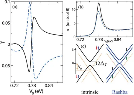
carrier with spin s [for Rashba SOC see the discussion below Eq.(7)]. Exact evaluations show (i)jγj>0for local SOCs of the intrinsic type, (ii) local Rashba SOCs induce jγj>0provided that electron-hole symmetry is broken by an electrostatic term, i.e.,V0≠0, and (iii)jγjis maximum
near resonances in Σs
∥. To illustrate these findings, we model the SOC active impurity as a uniform disk scatterer of radius R (see Fig. 1), according to VadðrÞ ¼
½V0þV
ðI=RÞ
SO 'ΘðR−rÞ, with Θð:Þdenoting the Heaviside step function and VðSOI=RÞ being intrinsic or Rashba-type SOC withΔ
I=RðrÞ≡Δ. The different symmetries of these
terms justifies studying them separately. Furthermore, it can be shown that interference between intrinsic and Rashba SOC does not suppress the resonant behavior of skewness (see the Supplemental Material [37]). In our calculations we have takenΔ∼10meV, which is consis-tent withab initiocalculations for metal atoms adsorbed in graphene [24,38]. The skewness of SOC active disk scatterers in the vicinity of a particular resonance is shown in Fig. 2. The function γðV0Þ follows an approximately
asymmetric shape for both intrinsic and Rashba SOC. We further note that for Rashba-only SOC the skewness approaches zero as V0→0 (not shown). We also found thatγis larger near sharp resonances, typically occurring at largeV0. It is known that small doses of certain adatoms
with large effectiveV0values produce resonances near the
Fermi level of graphene[31]that might dominate charge transport (see Ref. [39] for transport measurements in graphene covered with hydrogen). For dilute SOC disorder, the parameterγcan therefore be seen as a figure of merit for the capability of generating net transverse spin currents via skew scattering. In fact, as shown in what follows, in the absence of other sources of impurities and at zero temper-ature, the spin Hall angle equalsγ. Crucially, the results in Fig.2show that a largeV0is not a necessary condition to
obtain large skewness: although resonant impurities such as H induce giant effective potentials V0∼100eV (see
Ref. [31] and the references therein) and significant SOC via lattice distortion [23,32,36], clusters leading to
VSOof tens of milli-electron-volts most likely produceV0
values below those found for chemisorbed adatoms. Large
FIG. 1 (color online). Schematic picture of extrinsic spin Hall effect generated by transport skewness. An impurity (sphere) near the graphene sheet causes a local spin-orbit field with rangeR. The scattering of components with positive (negative) angular momentum is enhanced (suppressed) for charge carriers with sz¼1(sz¼−1), resulting in a net spin Hall current.
FIG. 2 (color online). Skew scattering induced by SOC impu-rities close to a resonance in the cross section. (a) Skeweness γ¼Σs
⊥=Σs∥ as a function ofV0 for an intrinsic (Rashba)-type
SOC scatterer [solid black line (dashed blue line)]. Even larger values ofγare found near sharper resonances occurring at larger V0 (not shown). (b) Transport cross section versus V0. These
[image:4.595.309.533.449.608.2] [image:4.595.62.287.548.652.2]SOC active scatterers could be formed by the clustering of physisorbed transition metals inducing significant local enhancement of SOC, such as Au or In[22,24].
After analyzing the SHE due to a single scatterer, we next turn to the experimentally relevant situation of a dilute random ensemble of scatterers. We focus on the spin Hall current polarized out of the plane; see the Supplemental Material [37] for a discussion of in-plane polarization. Our goal is to compute the spin Hall angle defined asθsH¼jsH=jx, withjx¼
P
s¼%js·exandjsH¼
P
s¼%sjs·ey being the expectation values of the (charge)
longitudinal and (spin) Hall currents, respectively. We safely neglect the quantum side-jump contribution to jsH, which is subdominant with respect to skew scattering in the dilute regime of interest here[40]. Semiclassically, the current is computed according to js¼
−egvPkδnsðkÞvk, where vk¼ ð1=ℏÞ∇kϵk is the band
velocity and δnsðkÞ ¼nsðkÞ−n0ðkÞ denotes the
deviation of the spin-dependent distribution function from its equilibrium value n0ðkÞ (g
v¼2 is graphene’s valley
degeneracy factor). To describe this situation, we need to solve the Boltzmann transport equation (BTE), which for the steady state in the presence of a uniform electric field E¼Eexreads as[41]
∇knsðkÞ·ð−eEÞ ¼ X
p;s0
½ns0ðpÞ−nsðkÞ'Ws0sðp;kÞ; (5)
where Wss0ðk;k0Þ∝jfss0ðθÞj2δðϵk−ϵk0Þ with θ¼
∠ðk;k0Þ is the quantum-mechanical rate for processes
with k→k0 and s→s0. Notice that skew scattering
implies that Wss0ðk;k0Þ≠Wss0ðk0;kÞ; cf. Eq. (3). Here, Wss0ðk;k0Þ≡PRα¼1WðssαÞ0ðk;k0Þ takes into account all disorder sources, where R≥1 is the number of such sources. In linear response, the above BTE admits the following general solution
δnsðkÞ ¼∇kn0ðkÞ·½AsðkÞeEþBsðkÞðzˆ×eEÞ'; (6)
where n0ðkÞ is the Fermi-Dirac distribution. With these
definitions, and at zero temperature, one finds
θsH¼B↑ðkFÞ=A↑ðkFÞ, wherekFis the Fermi momentum.
The latter expression can be evaluated in closed form:
θsHjT¼0¼ τ ( ∥ðkFÞ τ(⊥ðkFÞ
¼γ¯; (7)
where τ(∥−1¼Ps0;pð1−ss0cos θÞWss0ðk;pÞ and τ(⊥−1¼
P
s0;pss0sinθWss0ðk;pÞ. The spin Hall angleθsH equals the weighted skewness as defined by γ¯¼Σ¯(
⊥=Σ¯(∥, where
¯ Σ(
∥ð⊥Þ≡
P
αðnα=nÞΣ(∥ð⊥Þα¼ ðnvFτ
( ∥ð⊥ÞÞ−
1 and n¼P αnα
is the total areal density of impurities. The explicit solutions forAsðBsÞfurther contain the familiar scattering timesτ∥ andτ⊥ that do not enter in the ratioBs=As. The spin-flip
contribution to“star”rates differ from standard definitions, e.g., τ(−1
∥;flip∼
R
dθð1þcosθÞWss¯ðθÞ≠τ−∥;1flip. (For this reason, in the calculation of the skewness of a Rashba scatterer in Fig. 2 we have used Σ∥→Σ(
∥¼
P s0
R
dθð1−ss0 cosθÞjfss0
ðθÞj2.) This fact has been
largely unnoticed, which we believe is a consequence of inadequate treatments of the BTE; relaxation rates found here, on the other hand, result from the exact solution of linearized BTEs (see the Supplemental Material [37] for further details).
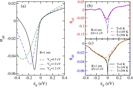
A sizeable SHE is expected in relatively clean samples when cross sections for SOC active scatterers yield the dominant contribution to both transport and skew cross sections; Fig.3showsθsH [Eq.(7)] as a function of Fermi energy for pristine graphene decorated with a dilute concentration of intrinsic-type SOC scatterers (θsHinduced by Rashba-type SOC is of the same order of magnitude and hence is not shown). The values obtained are comparable with those found in pure metals jθsHj∼0.01–0.1 [11,12]
and are robust with respect to thermal fluctuations and disorder averaging [compare curves in Figs.3(a)and3(c)]; room temperature spin Hall angles of the order of 0.1 are obtained for large scatterers with effective radius of just a few nanometers [see Fig.3(b)]. Statistical distribution of scatterer sizes does not modify qualitatively this picture, indicating that large SOC active scatterers in clean gra-phene samples will drive the formation of robust spin Hall currents. Finally, we verified that time-reversal symmetry breaking by localized magnetic moments[42]sitting at the impurities does not suppress the SHE (see the Supplemental Material [37]). Our findings suggest that functionalized graphene can be used to design spintronic integrated circuits with SHE-based spin-polarized current activation and control.
-0.15 -0.1 -0.05 0 0.05 θsH T=0 K T=149 K T=298 K
-0.4 -0.2 0 0.2 0.4
ε
F (eV)
-0.06 -0.04 -0.02 0 0.02 θsH
V0=0.5 eV
V0=1.0 eV
V0=1.2 eV
-0.4 -0.2 0 0.2 0.4
ε
F (eV)
-0.06 -0.04 -0.02 0 θsH T=0 K T=149 K T=298 K
∆V=2 eVR=1 nm
(a) ∆V=1 eV R=4 nm (b) (c) R=1 nm
FIG. 3 (color online). Spin Hall angle as a function of Fermi energy for a dilute random distribution of intrinsic SOC scat-terers. (a)θsHat zero temperature for impurities producing a local electrostatic potentialV0. (b),(c)θsHat different temperatures and considering a random V0 potential with uniform distribution
V0∈½0;ΔV'. In all panels we have takenΔI ¼25meV.
[image:5.595.310.531.505.651.2]A. F., M. A. C. and A. H. C. N. acknowledge support from the National Research Foundation–Competitive Research Programme through the grant“Novel 2D materi-als with tailored properties: beyond graphene” (Grant No. R-144-000-295-281). T. G. R. acknowledges support from INCT–Nanocarbono, CNPq, and FAPERJ. M. A. C. acknowledges support from NSC and start-up funding from NTHU (Taiwan). Discussions with N. M. R. Peres and A. Pachoud are gratefully acknowledged.
[1] M. I. Dyakonov and V. I. Perel, JETP Lett.13, 467 (1971). [2] J. E. Hirsch,Phys. Rev. Lett.83, 1834 (1999).
[3] S. Zhang,Phys. Rev. Lett. 85, 393 (2000).
[4] T. Jungwirth, J. Wunderlich, and K. Olejnik,Nat. Mater.11,
382 (2012).
[5] Y. K. Kato, R. C. Myers, A. C. Gossard, and D. D. Awschalom,Science306, 1910 (2004).
[6] V. Sih, R. C. Myers, Y. K. Kato, W. H. Lau, A. C. Gossard, and D. D. Awschalom,Nat. Phys.1, 31 (2005).
[7] K. Ando and E. Saitoh,Nat. Commun.3, 629 (2012). [8] S. O. Valenzuela and M. Tinkham,Nature (London)442,
176 (2006).
[9] T. Seki, Y. Hasegawa, S. Mitani, S. Takahashi, H. Imamura, S. Maekawa, J. Nitta, and K. Takanashi,Nat. Mater.7, 125
(2008).
[10] L. Liu, T. Moriyama, D. C. Ralph, and R. A. Buhrman,
Phys. Rev. Lett.106, 036601 (2011).
[11] L. Liu, C.-F. Pai, Y. Li, H. W. Tseng, D. C. Ralph, and R. A. Buhrman1,Science336, 555 (2012).
[12] M. Morota, Y. Niimi, K. Ohnishi, D. H. Wei, T. Tanaka, H. Kontani, T. Kimura, and Y. Otani,Phys. Rev. B83, 174405
(2011).
[13] K. S. Novoselov, A. K. Geim, S. V. Morozov, D. Jiang, M. I. Katsnelson, I. V. Grigorieva, S. V. Dubonos, and A. A. Firsov, Nature (London) 438, 197 (2005); Y. Zhang, Y.-W. Tan, H. L. Stormer, and P. Kim, Nature (London)
438, 201 (2005); A. H. C. Neto, F. Guinea, N. M. R. Peres,
K. S. Novoselov, and A. K. Geim,Rev. Mod. Phys.81, 109
(2009).
[14] N. Tombros, C. Jozsa, M. Popinciuc, H. T. Jonkman, and B. J. van Wees,Nature (London)448, 571 (2007). [15] S. Cho, Y. F. Chen, and M. S. Fuhrer,Appl. Phys. Lett.91,
123105 (2007).
[16] W. Han, K. Pi, K. M. McCreary, Y. Li, J. J. I. Wong, A. G. Swartz, and R. K. Kawakami,Phys. Rev. Lett.105, 167202
(2010).
[17] A. Avsar, T.-Y. Yang, S. Bae, J. Balakrishnan, F. Volmer, M. Jaiswal, Z. Yi, S. R. Ali, G. Güntherodt, B. H. Hong, B. Beschoten, and B. Özyilmaz,Nano Lett.112363 (2011). [18] B. Dlubak, M.-B. Martin, C. Deranlot, B. Servet, S. Xavier,
R. Mattana, M. Sprinkle, C. Berger, W. A. De Heer, F. Petroff, A. Anane, P. Seneor, and A. Fert,Nat. Phys.8, 557
(2012).
[19] D. Huertas-Hernando, F. Guinea, and A. Brataas,Phys. Rev.
B74, 155426 (2006).
[20] S. Konschuh, M. Gmitra, and J. Fabian,Phys. Rev. B82,
245412 (2010).
[21] D. Pesin and A. H. MacDonald,Nat. Mater.11, 409 (2012). [22] D. Marchenko, A. Varykhalov, M. R. Scholz, G. Bihlmayer, E. I. Rashba, A. Rybkin, A. M. Shikin, and O. Rader,Nat.
Commun.3, 1232 (2012).
[23] A. H. Castro Neto and F. Guinea, Phys. Rev. Lett.103,
026804 (2009).
[24] C. Weeks, J. Hu, J. Alicea, M. Franz, and R. Wu,Phys. Rev.
X1, 021001 (2011).
[25] V. K. Dugaev, M. Inglot, E. Y. Sherman, and J. Barnaś,
Phys. Rev. B 82, 121310(R) (2010); A. Dyrdał and J.
Barnaś,Phys. Rev. B86, 161401(R) (2012).
[26] C. L. Kane and E. J. Mele, Phys. Rev. Lett. 95, 226801
(2005).
[27] V. V. Mkhitaryan and M. E. Raikh,Phys. Rev. B77, 245428
(2008).
[28] A. C. Hewson, The Kondo Problem to Heavy Fermions
(Cambridge University Press, Cambridge, England, 1993). [29] G.-Y. Guo, S. Maekawa, and N. Nagaosa,Phys. Rev. Lett.
102, 036401 (2009).
[30] T. Stauber, N. M. R. Peres, and F. Guinea,Phys. Rev. B76,
205423 (2007); J. P. Robinson, H. Schomerus, L. Oroszlany,
and V. I. Fal’ko,Phys. Rev. Lett.101, 196803 (2008); T. O. Wehling, S. Yuan, A. I. Lichtenstein, A. K. Geim, M. I. Katsnelson,Phys. Rev. Lett.105, 056802 (2010). [31] A. Ferreira, J. Viana-Gomes, J. Nilsson, E. R. Mucciolo, N.
M. R. Peres, and A. H. Castro Neto, Phys. Rev. B 83,
165402 (2011).
[32] J. Balakrishnan, G. K. W. Koon, M. Jaiswal, A. H. C. Neto, and B. Özyilmaz,Nat. Phys.9, 284 (2013).
[33] L. E. Ballantine,Quantum Mechanics: A Modern Develop-ment(World Scientific, Singapore, 1998).
[34] T. G. Rappoport, B. Uchoa, and A. H. C. Neto,Phys. Rev. B
80, 245408 (2009).
[35] K. Pi, W. Han, K. M. McCreary, A. G. Swartz, Y. Li, and R. K. Kawakami,Phys. Rev. Lett.104, 187201 (2010). [36] M. Gmitra, D. Kochan, and J. Fabian,Phys. Rev. Lett.110,
246602 (2013).
[37] See Supplemental Material at http://link.aps.org/
supplemental/10.1103/PhysRevLett.112.066601for
techni-cal derivations, and additional discussions about the effects of time-reversal breaking and interference between spin-orbit coupling terms, about the choice of quantization axis, and about the limitations of perturbative scattering formalisms.
[38] J. Ding, Z. Qiao, W. Feng, Y.Yao, and Q. Niu,Phys. Rev. B
84, 195444 (2011).
[39] J. Katoch, J.-H. Chen, R. Tsuchikawa, C. W. Smith, E. R. Mucciolo, and M. Ishigami, Phys. Rev. B82, 081417(R)
(2010); Z. H. Ni, L. A. Ponomarenko, R. R. Nair, R. Yang,
S. Anissimova, I. V. Grigorieva, F. Schedin, Z. X. Shen, E. H. Hill, K. S. Novoselov, and A. K. Geim,Nano Lett.10,
3868 (2010).
[40] N. A. Sinitsyn,J. Phys. Condens. Matter20, 023201 (2008). [41] We have neglected spin coherence innsðkÞ, keeping only diagonal terms, which is expected to be a good approxi-mation at room temperature. We further note that the BTE does not describe transport close to the Dirac point. [42] M. B. Lundeberg, R. Yang, J. Renard, and J. A. Folk,Phys.