UNIVERSITI TEKNIKAL MALAYSIA MELAKA
STRENGTH ANALYSIS OF IC PACKAGE THROUGH THE
IMPACT OF DYNAMIC LOAD
This report submitted in accordance with requirement of the Universiti Teknikal Malaysia Melaka (UTeM) for the Bachelor Degree of Manufacturing Engineering
(Manufacturing Design) (Hons.)
by
NOOR’AIN BINTI AZIZAN
B051210073 931022-07-5640
DECLARATION
I hereby, declared this report entitled “Strength Analysis of Integrated Circuit Package through the Impact of Dynamic Load” is the result of my own research
except as cited in references.
Signature : ……… Author’s Name : NOOR’AIN BINTI AZIZAN
APPROVAL
This report is summited to Faculty of manufacturing Engineering of UTeM as a partial fulfillment of the requirements for the degree of Bachelor of Manufacturing Engineering (Manufacturing Design) (Hons.). The member of the supervisory committee is as follow:
i
ABSTRAK
ii
ABSTRACT
iii
DEDICATION
To my beloved mother and father and brother
KAIRON BEE BINTI MOHAMMAD HUSSAIN AZIZAN BIN ISMAIL
MUHAMMAD KHAIRUL AZLIZAN BIN AZIZAN
Supervisor
KHAIRUL FADZLI BIN SAMAT
iv
ACKNOWLEDGEMENT
First at all, I would like to express my greatest gratitude to Allah S.W.T., for His will, this project has finished completely. Thousands of thanks to my supervisor, En Khairul Fadzli Bin Samat for his kind and patience, his valuable advices, concern, guidance, time and support throughout the process to completing my degree project. I would also like to express my sincere gratitude to my parents and family, who had continuously giving out their support financially and emotionally for me to complete my project. Also a lots of thanks to my dearest friends and lectures for all the knowledge, helps and guidance to complete this project.
v
TABLE OF CONTENT
Abstrak i
Abstract ii
Dedication iii
Acknowledgement iv
Table of Content v
List of Table vii
List of Figures ix
List Abbreviations, Symbols and Nomenclatures xi
CHAPTER 1: INTRODUCTION 1
1.1 Background 1
1.2 Problem Statement 3
1.3 Objective 5
1.4 Scope 5
1.5 Project Schedule 6
CHAPTER 2: LITERATURE REVIEW 8
2.1 Overview of IC Package 8
2.1.1 Type of IC Package 8
2.1.2 Component in IC Package 9
2.1.2.1 Mould 9
2.1.2.2 Diepad 10
2.1.2.3 Die 11
2.1.2.4 Die attach 11
2.1.2.5 Wirebonds 12
2.1.2.6 Lead 13
2.1.3 The DSO14 Package 14
2.2 Pogo Pin 15
2.3 3D Model and Simulation Analysis 17
vi
2.3.2 Finite Element Analysis 17
2.3.3 ANSYS Software 20
2.3.3.1 Mesh Convergent Analysis 21
2.4 Dynamic effect 22
2.4.1 Explicit Dynamic 22
2.4.2 Theories of Strength Analysis 22
2.4.3 The Strength of Silicon Die 24
CHAPTER 3: METHODOLOGY 29
3.1 Major Dimension and Modelling 31
3.2 Discretization 33
3.2.1 Mesh Geometry 33
3.2.2 Explicit Dynamic 34
3.3 Material 35
3.3.1 Material Properties 35
3.3.2 Stress-strain Diagram of C19400 36
3.3.3 The Assumption on Behaviour of the Material 37
3.4 Loading and Boundary Conditions 37
3.4.1 Orientation Setup 37
3.5 Finite Element Simulation-Dynamic 40
3.5.1 Calculation of Initial Setup of Finite Element Simulation 40 3.5.2 Establishment of Initial Setup of Finite Element Simulation 41 3.5.2.1 Geometry Model and Mesh Optimization 41 3.5.2.2 Time Travel of Pogo Pin during Simulation 43
3.5.3 Mesh Convergence Study 44
CHAPTER 4: RESULTS AND DISCUSSION 45
4.1 Verification of Developed Model 45
4.2 Validation of Experimental Study 47
4.3 Extend Analysis of Model to other Conditions 49
vii
CHAPTER 5: CONCLUSION AND FUTURE WORK 56
5.1 Conclusion 56
5.2 Future Work 57
5.3 Sustainable for the Project 57
viii
LIST OF TABLES
1.1 Project Schedule for PSM 1 6
1.2 Project Schedule for PSM 2 7
2.1 Dimension of Pogo Pin Component 16
2.2 Material of Barrel-less Pogo Pin 17
3.1 The Total Number of Nodes and Element in Meshing 34 3.2 Material Properties for Every Component 35
3.3 Possible Condition on Each Parameter 38
3.4 Description of Velocity and Boundary Condition for Every Orientation
of Tests 39
3.5 Analyze the time travel of the pogo pin 43
ix
LIST OF FIGURES
1.1 Quad Flat Packs Once of IC Package Example 1
1.2 Experiment Equipment 3
1.3 Factor that Effect the IC Package 4
2.1 Type of IC Package 9
2.2 Step of Making Mould of IC Package 10
2.3 Relation between Thickness and Strength of Die 11
2.4 Die Attach inside the IC Package 12
2.5 Wirebond in IC Package 13
2.6
Gold Wire Connecting to Lead Frame 14
2.7 DSO14 Non-exposed Die 14
2.8 DSO14 Exposed Die 14
2.9 DSO14 Heatslug 15
2.10 Pogo Pin 15
2.11 Detail Drawing of Pogo Pin 16
2.12 Barrel-less Pogo Pin 16
2.13 The Procedure of FEA Process 18
2.14 Classification of Common Methods 18
2.15 Simulation using Explicit Dynamic 22
2.16 Relationship between the External Force and the Maximum
Principal Stress 26
2.17 Schematic Drawing of a Three-point Bending Test 26
2.18 Linear Elastic Stress Analysis 27
2.19 Piezoresistive Sensors Concept 28
3.1 Project Flow 30
3.2 The Major Dimension of IC Package 31
3.3 The Dimension of Die/Chip 31
3.4 IC Package Description with Exposed Diepad 32 3.5 3D Model of IC Package in Wireframe View 32 3.6 The General Flow for Discretization 33
3.7 Meshing Model 34
3.8 Schematic Diagram for Internal Structure of IC Package 35
3.9 Stress-strain Curve for C19400 37
3.10 Example of Possible Orientations of Exerted Velocity and Support 38
3.11 Effective Area of the Load 40
3.12 Area of Plunger 40
3.13 3D Model Pogo Pin 42
x 3.15 The Distribution of Stress by Rigid (left) and Flexible (right)
Pogo Pin Condition 42
3.16 Time Travel of Pogo Pin 43
4.1 Equivalent Von Misses Stress of Diepad 46
4.2 Maximum Principle Stress of Die 47
4.3a Dent Mark Appear in Experimental Study 48 4.3b Distribution Stress on Diepad using ANSYS prove that have
Plastic Deformation 48
4.4a Crack Occur in Die Surface 49
4.4b Distribution Maximum Principle Stress on Die using ANSYS
prove that have Possible Crack 49
4.5 Equivalent Von Misses Stress for All Conditions 51 4.6 Maximum Principle Stress for All Conditions 52
4.7 Cross Section of Meshed Geometry 53
xi
LIST OF ABBREVIATIONS, SYMBOLS AND
NOMENCLATURE
Al - Aluminium
Au - Gold
DIP - Dual In-line Package DSO - Dual Small Outline EFO - Electric flameoff
FBGA - Fine-pitch ball grid array FEA - Finite Element Analysis IC - Integrated circuit PCB - Printing circuit board RPM - Rotation per minute
Si - Silicon
TCE - Temperature coefficient of expansion > - More than
~ - Nearest
σ - Stress
ϵ - Strain
1
CHAPTER 1
INTRODUCTION
In this chapter, it contains a brief explanation about the background of this project which is, “Strength Analysis of Integrated Circuit Package through the Impact of Dynamic Load”. This chapter are consists the background of project, problem statement, objective and scope.
1.1 Background
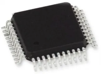
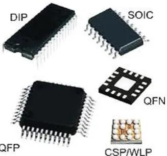
[image:15.595.240.403.612.731.2]In electronic worlds, integrated circuit (IC) package is a protective package that function to easy the hold and assembly onto printed circuit boards, also defend the devices from crack or damage. In IC package consist of die that function for direct connections to a substrate without an intermediate header or carrier. Three general categories of IC package which are Dual In-line Packages (DIP), Quad Flat Packs and Grid Arrays. All the packages have a body style that scales with pin count, for examples DIP with the two rows of lead on two sides of the package, Quad Flat Packs with leads on all four sides (Figure 1.1) and Grid Arrays that have pins arranged in a grid (www.electroons.com).
2 Since the IC packages are manufactured by several materials, it will have the certain failure theories. In other hand, the major material use for die/chip is silicon. Silicon is brittle material that has a lower of yielding because of crystal structure. In crystal structure behavior, it will not allow in plastic deformation compare to layer structure. This characteristic will cause the cleavage inside the die when occur by impact of load. Therefore, the properties of die been investigated by experimental or simulation due to different dimension built with advance of technology (Cornelis Klein, 1985).
Pogo pin is used to connect the electrical between IC lead and load board. There are several problems using pogo pin which are indentation marks, blur marks, tilting spring and high cost. It also cause a reliability problems when dealing-pitch packages. The contact of pogo pin and IC package will have the foreign particle that will affect the surface of IC package. There are also several effects that produced by pogo pins which are the force been applied during production and the impact of velocity on the IC package. Therefore, at the end of production the test need to conduct to check the IC package condition. In manufacturing of semiconductor, there were many process that may effects at the end of production. Therefore, the test on IC package had been applied to make sure all requirement connection and performance are fulfilled (M.Idzdihar Idris, 2015).
The physical test shows the visual failure that currently occurs in electronic device. The common tests that have been used in IC package device are point-load test, three-point bending and four-point bending test. These three tests were purpose to investigate the reliability of chip (M.Y. Tsai, 2008).
Free drop test is the method that used to investigate drop test respond and for sight and electrical failures after the drop test. Data from experiment can get the impact of stress wave propagation and distribution to an IC packages (Scott Irving, 2004).
3 affordably find the state that provides sufficient survivability under different states of condition. This method is used to detect failure stress on the die due to several limitations which are the cost, finding distribution of stress and close assumption to the real impact (Jiang Yuqi, 2005).
1.2 Problem Statement
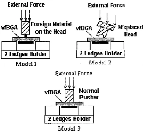
[image:17.595.214.423.348.668.2]There are some problem arise during the testing process of IC package as shown in Figure 1.2. Therefore, have a several factors that might be contribute toward to the problem of IC package such as foreign particles, assembly speed, split of pogo pin. The illustration of the factor that effect the IC package are shown in Figure 1.3.
4 Figure 1.3: Factor that Effect the IC Package (Fang Yu, 2002)
5 1.3 Objective
The aim of this project is to analyze the strength analysis of IC package through the impact of dynamic load. This can be carried out through these objectives:
1. To study the internal stress generated in 3D model of IC package due to dynamic impact of pogo pin.
2. To find out the possibility of die crack in IC package by dynamic impact of pogo pin.
3. To extend the strength analysis of die and diepad on the several conditions.
1.4 Scope
6 1.5 Project Schedule
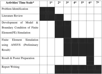
[image:20.595.112.531.238.542.2]Table 1.1 shows the project schedule for PSM 1 that has to achieve according to the plan. There are several identifications and researches have been done for this project. For PSM 1, the model of project has been constructed and the boundary condition of finite element simulation also has been considered. The preliminary result has been analyzed using ANSYS software. Poster presentation for this project and the writing of report from Introduction to Methodology was done according to project schedule.
Table 1.1: Project Schedule for PSM 1
Activities/ Time Scale* 1* 2* 3* 4* 5* 6* 7*
Problem Identification
Literature Review
Development of Model & Boundary Condition of Finite Element(FE) Simulation
Finite Element Simulation using ANSYS (Preliminary Result)
Result & Poster Preparation
Report Writing
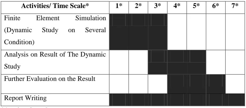
7 Table 1.2 shows the project schedule for PSM 2 that also has to achieve according to the plan. The study of dynamic on several conditions has been done using ANSYS software. The analysis and further evaluation on result have been done according to schedule. Finally report writing be edit and done before due date of submission.
Table 1.2: Project Schedule for PSM 2
Activities/ Time Scale* 1* 2* 3* 4* 5* 6* 7*
Finite Element Simulation (Dynamic Study on Several Condition)
Analysis on Result of The Dynamic Study
Further Evaluation on the Result
Report Writing
8
CHAPTER 2
LITERATURE REVIEW
2.1 Overview of IC Package
IC package is a protective package use to cover the inside semiconductor material from damage and crack. Another functions of IC package are to facilitate the packaging and handling of IC chip, to dissipate heat generate by IC package and protect the IC package characteristic. It usually place in circuit boards to the external electronic or electric device. Inside the IC package, there was die that need to been protecting. It the higher in power because of eutectic bonded into the package and made using silicon. It directly glued using adhesive (Diego & Development, 2001).
2.1.1 Type of IC Package
9 Figure 2.1: Type of IC Package (Diego & Development, 2001)
2.1.2 Component in IC package
There are six component in the IC package which are mould, diepad, die, die attach, wireframe and lead.
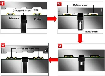
2.1.2.1 Mould
[image:23.595.239.403.75.228.2]10 Figure 2.2: Step of Making Mould of IC Package (www.daiichi-seiko.com)
Material that been used were ceramic and plastic packages. It been selected based on their application and operating environment. If ceramic, it has high reliability while plastic most popular because of low cost. IC package classified based on shape, material, and mounting methods (Diego & Development, 2001).
2.1.2.2 Diepad
[image:24.595.135.503.69.335.2]