Article
Design of Visible Light Communication Receiver for
On-Off Keying Modulation by Adaptive
Minimum-Voltage Cancelation
Yan Zhao
*and Jayakorn Vongkulbhisal
International School of Engineering, Faculty of Engineering, Chulalongkorn University, Bangkok 10330, Thailand
*E-mail: [email protected]
Abstract. In this paper, a new design of visible light communication (VLC) receiver for on-off keying (OOK) modulation is proposed. The design is based on the cancelation of minimum offset voltage of the received OOK signal, using a novel minimum-voltage detection circuit. This circuit is capable of tracking the minimum voltage of an input signal even if its value increases with time. Experimental results show that the proposed receiver is immune to the interference from sunlight and indoor fluorescent lights.
Keywords: Minimum-voltage cancelation, on-off keying (OOK), visible light communication (VLC).
ENGINEERING JOURNAL Volume 17 Issue 4 Received 4 April 2013
1.
Introduction
Optical wireless communication (OWC) refers to the wireless transmission of electronic data via a light wave carrier [1]. Typical optical sources in OWC systems include high power solid state lasers or diode lasers. With the recent advances in the semiconductor technology, these sources can be replaced by light emitting diodes (LEDs), especially for short and medium-range applications. Systems using visible light as carriers are termed as visible light communication (VLC) systems [2]. For indoor environments, VLC systems provide a low cost, high speed, power efficient, and secure solution to data transmission in addition to lighting. VLC systems may find their applications in healthcare, aviation, underwater communications, and location based services [3] etc.
Recently, the OWC using visible light has been standardised by the Institute of Electrical and Electronics Engineers (IEEE) [4]. The on-off keying (OOK) modulation scheme specified in this standard is simple to implement [5], however it often suffers from the interference caused by ambient lights. At the receiver, received optical signals typically contain the modulated OOK signal, a direct current (DC) component from the sunlight, and a rectified sine wave emitted from indoor fluorescent lights (its frequency is double of the power grid’s) [6]. The DC component from the sunlight and the rectified sine wave cannot be removed by using capacitors or applying high-pass filtering, as the OOK signal itself also contains a significant DC component.
Essentially, the interference from ambient lights is of additive nature to the modulated information, and all the received optical signals are superimposed together. Hence once the interference level is known at the receiver, the modulated signal can be directly recovered. For the case of OOK modulation, as zero and a high voltage are used to represent digital ‘0’ and ‘1’, the minimum voltage of the OOK signal directly represents the additive interference. Based on this concept, we propose a new VLC receiver design for removing the interference from ambient lights for OOK modulation. In order to track the minimum voltage, an adaptive minimum-voltage detection circuit is also proposed.
2.
Visible Light Communication Receiver Design
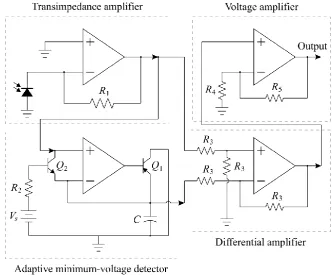
[image:2.595.120.478.493.580.2]As shown in Fig. 1, the designed VLC receiver contains four parts: a transimpedance amplifier (TIA) for converting optical signals to electrical voltage, the proposed adaptive minimum-voltage detector (AMD) for tracking the minimum value of the converted voltage signal, a differential amplifier (DA) for removing the minimum voltage, and a voltage amplifier (AMP).
Fig. 1. System block diagram of the proposed VLC receiver.
The TIA, DA, and AMP are standard and well-known circuit designs. For the adaptive minimum-voltage detector, the conventional non-adaptive (or semi-adaptive) design (Fig. 2, bottom left part without Q2, R2 and Vs) performs well when its input is a stable OOK signal, or the signal’s minimum amplitude
decreases with time. The voltage across the capacitor C is the same as the voltage at the negative input (‘–’) terminal of the operational amplifier (op amp), and the PNP transistor Q1 acts as a switch. When the
voltage at the positive input (‘+’) terminal of the op amp is higher than the voltage across C, the op amp outputs current and Q1 is ‘off’. On the other hand, when the voltage at the ‘+’ terminal is lower than the
voltage across C, Q1 is turned ‘on’ and C is discharged to the same voltage as the ‘+’ terminal. Therefore
Fig. 2. Schematic diagram of the proposed VLC receiver.
Due to the above mentioned constrains, we propose to include additional components Q2, R2 and Vs,
in order to charge the capacitor when the minimum amplitude of the signal increases. In our design, an NPN type bipolar junction transistor (BJT) is connected between the (‘+’) and (‘–’) terminals of the op amp. It is worth noting that diode cannot be used in place of the BJT, as the charging rate cannot be controlled. Ideally, charging is only required during the low-amplitude bit period of the OOK signal, and also when the low amplitude increases with time. However, as it is impossible to predict when the low amplitude of a random OOK signal arrives at the input, a DC source Vs is used, meaning that the capacitor is being constantly charged through Q2.
The charging/discharging rate of C depends on both the emitter currents of Q1 and Q2, and the
capacitance of C. When the voltage at the ‘+’ terminal is lower than that at the ‘–’ terminal, the emitter current of Q1 must be larger than that of Q2 to ensure that C can be discharged promptly, thus the
resistance of the current-limiting resistor, R2 must be large. When the voltage at the ‘+’ terminal is higher
than that at the ‘–’ terminal, Q1 is off, and the emitter current of Q2 cannot be either too low for the voltage
across C to reach a new (higher) minimum amplitude during one bit period of the OOK signal, or too high so that the voltage rises too much above the minimum amplitude. From the above discussion, for our adaptive design to be able to track the minimum voltage, it is necessary to find an appropriate capacitance of C according to the bit rate of the input OOK signal.
[image:3.595.129.462.77.352.2]In the current work, the designed VLC receiver for 1 Mbit/s OOK signals is simulated using National Instruments’ Multisim and fabricated on a double-sided printed circuit board (PCB), as shown in Fig. 3. The op amps are selected for their wide bandwidth and high slew rate, in order to process high data rate OOK signals. Two voltage converters are also included in the design as power supplies for the op amps. The values of other components are listed in Table 1, where the optimum capacitance value of C is found from Multisim simulations.
Table 1. Values of resistors and capacitor for the designed VLC receiver for 1 Mbit/s OOK signals.
Element R1 R2 R3 R4 R5 C
Fig. 3. Fabricated VLC receiver circuit using adaptive minimum-voltage cancelation: Top view (left) and back view (right).
3.
Measurement Results and Discussion
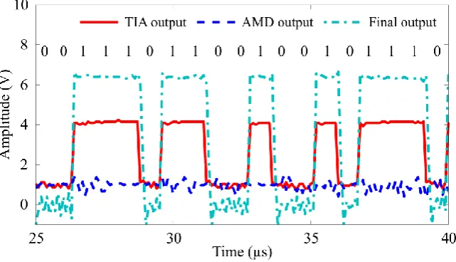
[image:4.595.116.479.78.251.2]Experiments on the fabricated VLC receiver are performed using a universal serial bus (USB)-to-serial interface – the FTDI's FT2232H Mini-Module, driving a commercial high-brightness LED (HBLED) lamp through a high-speed op amp. The built-in control circuit of the HBLED lamp has been removed to enhance its switching speed. The tests are conducted in a room with windows and the fluorescent lights are switched on. OOK signals generated from random binary data sequences with a bit rate of 1.25 Mbit/s are sent from a computer through the FT2232H Mini-Module to the HBLED. The output voltage signals at different stages of the VLC receiver placed at 1 m away from the HBLED lamp are recorded on an oscilloscope and plotted in Fig. 4.
Fig. 4. Output waveforms from the fabricated VLC receiver when the it is placed away from the window.
[image:4.595.138.459.436.620.2]Fig. 5. Output waveforms from the fabricated VLC receiver when the it is placed near the window.
4.
Conclusion
A new VLC receiver design for OOK modulation is proposed in this paper. The design is based on the cancelation of minimum offset voltage of the input OOK signal, in order to remove the interference from ambient lights. Experiments show that the proposed VLC receiver is insensitive to sunlight and indoor fluorescent lights.
References
[1] S. Hranilovic, Wireless Optical Communication Systems, Springer, 2005.
[2] Y. Tanaka, S. Haruyama, and M. Nakagawa, “Wireless optical transmission with the white colored LED for the wireless home links,” Proceedings of the 11th IEEE International Symposium on Personal Indoor and Mobile Radio Communications, vol. 2, pp. 1325-1329, 2000.
[3] J. Vongkulbhisal, B. Chantaramolee, Y. Zhao, and W. S. Mohammed, “A fingerprinting-based indoor localization system using intensity modulation of light emitting diodes,” Microwave and Optical Technology Letters, vol. 54, pp. 1218-1227, 2012.
[4] IEEE Standards Association, IEEE Standard for Local and metropolitan area networks - Part 15.7: Short-Range Wireless Optical Communication Using Visible Light (IEEE Std 802.15.7), 2011.
[5] J. K. Kwon, “Inverse source coding for dimming in visible light communications using NRZ-OOK on reliable links,” IEEE Photon. Technol. Lett., vol. 22, pp. 1455-1457, 2010.