Rochester Institute of Technology
RIT Scholar Works
Theses Thesis/Dissertation Collections
5-2017
Vedic Based Division Core Design
Ryan Hinkley
Follow this and additional works at:http://scholarworks.rit.edu/theses
This Master's Project is brought to you for free and open access by the Thesis/Dissertation Collections at RIT Scholar Works. It has been accepted for inclusion in Theses by an authorized administrator of RIT Scholar Works. For more information, please [email protected].
Recommended Citation
VEDIC BASEDDIVISIONCORE DESIGN
by
Ryan Hinkley
A Graduate Paper Submitted
in
Partial Fulfillment
of the
Requirements for the Degree of
MASTER OFSCIENCE
in
Electrical Engineering
Approved by:
PROF.
(GRADUATEPAPERADVISER- MARKA. INDOVINA)
PROF.
(DEPARTMENTHEAD- DR. SOHAILA. DIANAT)
DEPARTMENT OFELECTRICAL AND MICROELECTRONICENGINEERING
COLLEGE OFENGINEERING
ROCHESTER INSTITUTE OF TECHNOLOGY
ROCHESTER, NEWYORK
I would like to dedicate this work to my family, Sue, Don, Kara, and Abby for all their love and
support throughout my entire life, and also to my friends for their love and inspiration
Declaration
I hereby declare that except where specific reference is made to the work of others, that all
content of this Graduate Paper are original and have not been submitted in whole or in part for
consideration for any other degree or qualification in this, or any other University. This Graduate
Project is the result of my own work and includes nothing which is the outcome of work done in
collaboration, except where specifically indicated in the text.
Ryan Hinkley
Acknowledgements
I would like to thank my adviser, Mark A. Indovina, for his support, guidance, and feedback
through the past two years in both classes and in completion of this graduate paper. I would
also like to thank my colleague Julia Okvath for her assistance in finalizing this work. I am also
thankful for my other teachers that have taught me throughout my five years of college. Without
Abstract
Processors and embedded systems perform algebraic manipulations such as addition,
subtrac-tion, multiplication and division on integers in order to complete and execute programs.
Unfor-tunately, most division cores in these devices take significantly more time to compute than other
manipulations. Because of this, research has been conducted on finding a division algorithm that
does not take as long to execute. This graduate paper discuses and proposes a division core
de-sign based on ancient Vedic mathematics. The dede-sign is created and simulated as a 4-bit system
for completion and analyzed for timing, power consumption, and cell area usage. Estimations
on larger designs are completed and used to compare this design to similar ones. It is found
that the timing and cell area usage are very minimal compared to other designs based on the
same algorithm. However, the power consumption is significantly higher. Possible optimizations
and improvements to the design are proposed for future use. At the end of this graduate paper,
Contents
Contents v
List of Figures vii
List of Tables viii
1 Introduction 1
1.1 Research Goals . . . 1
1.2 Contributions . . . 2
1.3 Organization . . . 3
2 Preliminaries and Background Research 4 2.1 Pipelined System . . . 4
2.2 Vedic Division Algorithm . . . 4
2.3 Similar Architectures . . . 7
2.4 Verilog . . . 7
2.5 Python . . . 8
2.6 Simulation and Analysis Software . . . 8
Contents vi
3.1 Single Manipulation Algorithm . . . 11
3.2 Final Manipulation Algorithm . . . 14
4 Simulation and Evaluation of the 4-bit Architecture 17 4.1 Simulation . . . 17
4.2 Timing Analysis . . . 18
4.3 Power Consumption Analysis . . . 18
4.4 Area Usage Analysis . . . 21
5 Future Work 24 5.1 Future and Complex Implementations . . . 24
5.2 Optimizations . . . 28
6 Conclusion 29
References 31
I Verilog Design Code 33
List of Figures
2.1 Paravartya Sutra in the decimal number system . . . 5
2.2 Paravartya Sutra in the binary number system . . . 6
2.3 Paravartya Sutra in the binary number system . . . 6
3.1 Overall Algorithm . . . 10
3.2 Data flow . . . 10
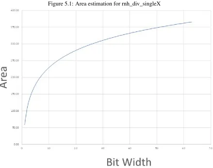
5.1 Area estimation for rnh_div_singleX . . . 25
List of Tables
4.1 Power consumption distribution . . . 19
4.2 Power consumption by module . . . 20
4.3 Cell area by module . . . 21
Chapter 1
Introduction
Computers at their lowest level are just bit manipulators. They conduct arithmetic operations to
process, compute, and evaluate binary numbers. These numbers can be ASCII characters, pixel
colors, condition values for operations, and many more identifiers. The most common operations
are addition, subtraction, and logic AND, OR, and NOT. Part of the reason for these operations
are their simplicity and ability to compute the data in a short period of time. However, many
processors use additional operations to compute greater amounts data efficiently and effectively.
Examples of these operations are multiplication and division. However, to use these operations,
large arithmetic blocks must be designed for each function and most likely have a latency in their
output to the device. This paper describes a pipe-lined division core that can be used in this case.
1.1
Research Goals
The first goal of this graduate paper is to research and understand a division algorithm and then
use the algorithm to design a division core. The design will consist of Boolean logic formulas
1.2 Contributions 2
work in a pipe-lined system and on the uniqueness of the actual design.
The second goal of this work is to create, simulate, and analyze using Verilog. The analysis
will include an investigation on timing, power consumption, and cell area usage which using
software. This will be used to predict the behavior and model of larger designs using the same
algorithm.
The third, and most important goal of this paper, is to determine if the chosen algorithm could
be successful when implemented in an actual processor or other devices. This will be done by
analyzing the output data and complexity of the final design.
1.2
Contributions
The first contribution is the research of possible algorithms that can be applied to a pipe-lined
division core and creation of a logic design based on this algorithm. Extensive research is
com-pleted in the search of algorithms that can be easily pipe-lined and modeled using Boolean logic.
The algorithm must also have the ability to scale from different size bits ranging from small to
large. In addition, choosing an algorithm that is not as well-known will create a more unique and
possibly better division core. From the chosen algorithm, a logic based design is created. This
design is modeled using a hardware description language (HDL) which is easily simulated and
analyzed.
The second contribution of this research refers to the simulation of the design. A test bench
generator must be created to output a test bench that simulates all possible combinations. This is
created using a high-level programming language. The string manipulation abilities of this
soft-ware allows for a simple text file containing every combination to be converted into an accurate
test bench with inputs and output verification.
1.3 Organization 3
model and implementations. Due to limitations, only a small model is created, simulated, and
analyzed. Because of this, the larger sized division cores’ timing, power consumption, and cell
area are estimated. These predictions are used to justify and conclude the usefulness of this
algorithm as a pipe-lined division core.
All contributions are completed and analyzed together to prove whether or not this algorithm
could be successful if implemented in an actual processor. This research will provide possible
choices for the algorithm and lead to an actual digital design. Simulations prove the accuracy of
the design. Lastly, the analysis of the output data will lead to the conclusion and verdict about
the successful implementation of the algorithm.
1.3
Organization
The organization of this graduate paper is as follows: Chapter 2 will discuss the background and
preliminaries related to the proposed design’s evaluation. Chapter 4 proposes the architectures
for the Vedic division algorithm. Chapter 5 presents the simulation and attribute results. Further
developments to the design with predictions to large-scale models of the system are given in
Chapter 2
Preliminaries and Background Research
Division algorithms from all around the world and history were considered as a possibility for
this paper. In addition, research was done to help complete the task. The research conducted is
presented below.
2.1
Pipelined System
A pipelined system is defined as a form of parallelism within a single core. It provides a faster
throughput than in a sequential system where one manipulation finishes before another one is
started[1]. The pipelined component of the designed division core will be that it computes
mul-tiple elements at a time. However, it can only take in one input and output one value at a time.
2.2
Vedic Division Algorithm
The chosen division algorithm used to compute both the divisor and remainder is based on Vedic
mathematics. Vedic mathematics are the mathematical functions used in the Vedic period
2.2 Vedic Division Algorithm 5
Divisor Dividend
1 2 5 2 3 7 1
-2 -5 -4 -10
2 5
2 -1 -1 6
[image:15.612.204.411.102.192.2]20-1-1=18 125-10+6=121
Figure 2.1: Paravartya Sutra in the decimal number system
time in history[3]. Arithmetic used in this period was not for computation in processors, it was
for rituals. One ritual required a fire-altar to be created that has a square base with five layers of
bricks and 21 bricks in each layer. They would have to divide one square into three equal parts
and that part into seven smaller parts[4]. This may seem simple for today’s algebra, but at the
time, it was revolutionary.
The chosen algorithm is a special case of synthetic division called the Paravartya Sutra[5].
Synthetic division is a short cut method for dividing a polynomial by a linear divisor[6].
Fortu-nately, the algorithm is compatible with pipelining. One element is computed at a time and is
used in the computation of the next element. Figure2.1shows an example in the decimal number
system where the number 2371 divided by 125.
Essentially, the most significant bit/digit (MSB) of the divisor is dropped and the rest of the
digits are negated. The negated part is multiplied by the MSB of the dividend and added to the
next set of MSBs. Then the negated part is multiplied by the total number in the second MSB
of the dividend. This last step repeats until it fills the length of the dividend. The length of the
negated part of the divisor determines the number of digits that correspond to the remainder (R).
The other digits represent the quotient (Q).
All the digits are summed and result the quotient and remainder. Because the remainder is
purely negative, 1 must be subtracted from the quotient. To determine the positive remainder,
2.2 Vedic Division Algorithm 6
Divisor Dividend
1 0 0 1 1 0 0 0 0 1 1 0 1
0 0 -1 0 0 -1
0 0 0
0 0 0
0 0 1
0 0 0
0 0 -1
1 0 0 -1 0 1 10 0 0
[image:16.612.179.434.100.249.2]Q=100001-10=11101 R=1000
Figure 2.2: Paravartya Sutra in the binary number system
Divisor Dividend
1 1 0 0 1 1 0 0 0 1 0 0 1
-1 0 -1 -1 0 0
0 0 0
0 0 0
0 0 0
0 0 0
-1 0 0
1 0 0 0 0 1 -1 0 1
Q=100001-1=100000 R=1100-100+1=1001
Figure 2.3: Paravartya Sutra in the binary number system
remainder are added (i.e.125−10+6=121) [7].
This algorithm is very confusing at first with the cases for negatives and positives, but the
simplicity and ability to be a pipelined system makes it worthwhile to implement. An example
of the algorithm in the binary number system is shown in figure2.2 where 269 divided by 9 is
calculated.
Another example is outlined in figure 2.3 where the division of 12 into 393 occurs. In this
case, the first bit of the remainder is negative. To calculate the remainder, all negative bits are
subtracted from the divisor and the positive bits are added. Also, an additional 1 is subtracted
[image:16.612.168.442.279.433.2]2.3 Similar Architectures 7
2.3
Similar Architectures
Similar designs have been made based on the Vedic division algorithm.
In one design, the dividend is a 16-bit binary number and the divisor was 8-bits. The delay is
only about 10.5nsand only consumes about 24µW with a layout area of about 10.25mm2[8].
Another design shows different computation speeds for different size dividends and divisors.
The 16-bit system’s longest output time is only 3.9µscompared to the worst case of 49.290µs
for the non-restore or normal division algorithm[9].
2.4
Verilog
Verilog is one of the most popular hardware description languages (HDLs) with the others being
SystemVerilog and VHDL. Verilog is used to create the proposed design in this paper. HDL is
a language that supports the early conceptual stages of design with its behavioral and structural
abstractions[10]. Verilog contains hierarchical constructs that allow the designer to control the
complexity of the design. Verilog was first created in 1983-84 as a proprietary verification and
simulation product by Phil Moorby. Eventually, synthesis and timing analyzer tools were added
to the language. Input specification for logic and behavioral synthesis tools were also added later.
Verilog was standardized by IEEE in 1995 (IEEE Standard: 1364-1995) and revisited again in
2001 (IEEE Standard: 1364-2001) and 2005 (IEEE Standard: 1364-2005)[11].
Verilog can be used to design and test register transistor level (RTL) circuit. The test is
called a test-bench. The most common test-benches simulate different inputs into the design and
checks the outputs for correctness. Different simulation software packages allow the user to view
internal signals as well as the input and output signals. A good test-bench checks many different
input values especially at all the extreme inputs.
2.5 Python 8
2.5
Python
Python is a widely used high-level programming language. It was first implemented in 1989 [12]
with the design philosophy of emphasizing on code readability[13]. This is shown in the code
by the white-space and indentation instead of using brackets (that are used in C) or keywords
(such as ’begin’ and ’end’ in Verilog). One of the other unique traits about Python is that type
constraints, such as “int” or “string”, are not checked at compile time because they are assigned
as needed.
A Python 2 script is used to create a test bench by reading a simplified text file. Python 2.0
was released on October 16th, 2000[14]. The script converts simple division value, such as 15/4, into an input to the division module. The same generated testbench also checks for the output of
the division statementxclock cycles later wherexis the number of bits of the division module.
2.6
Simulation and Analysis Software
The design is both simulated and analyzed in this paper for correctness and operation.
The software used for simulation is Incisive Suite which includes SimVision (64)
15.10s-014[15]. SimVision is a graphical debugging environment developed and distributed by Cadence
Design Systems. The software lets the user view individual waveforms of internal signals in the
system throughout the entire run-time. This software is very useful in determining whether
signals are correct or incorrect at any given time in the design.
For logic synthesis, DC Ultra is used. DC Ultra RTL synthesis is a software tool that
com-putes timing, area, power, and test optimization concurrently and is developed and distributed
by Synopsys. Synopsys has documented that the software gives results that correlate to physical
implementations within 10% error[16]. This software will be used to calculate the timing, cell
Chapter 3
Binary Division Algorithm Implementation
The preliminaries for the Vedic division algorithm are presented in this chapter. The different
components of the algorithm are separated into each individual step and the final step. The
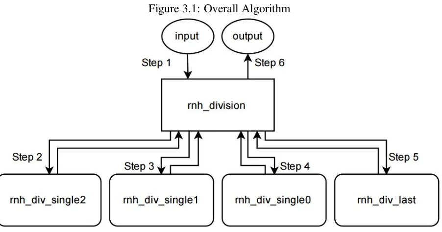
overall design of this system is summarized in figure3.1.
Figure 3.1 shows 6 different steps that are executed in the algorithm. The first step is to
read in the input. The second, third, and fourth are to manipulate the dividend, carry, and sign
bit using the single manipulation algorithm. Step 5 is the execution of the final manipulation
algorithm and the final step, step 6, is to output the quotient and remainder.
The movement of data from each step is shown in figure 3.2. The figure shows the flow of
the four main registers, which are the divisor, dividend, sign, and carry, throughout the design.
The divisor remains the same and only the dividend, carry, and sign values change. The only
other registers that get assigned values are the quotient and remainder registers at the end. It is
also seen that the system can easily be used as a pipeline. Steps 2 through 5 represent a different
clock cycle in the pipeline with continuous inputs from dividend_in and divisor_in and an output
10
Figure 3.1: Overall Algorithm
[image:20.612.82.533.167.404.2]3.1 Single Manipulation Algorithm 11
3.1
Single Manipulation Algorithm
This section focuses only on the single step algorithm that is takenN−1 times where N is the
number of bits. This algorithm gets more complicated as the number of bits increases, but the
main algorithm stays roughly the same throughout. The modules that use this algorithm are
named “rnh_div_single0”, “rnh_div_single1”, and “rnh_div_single2” with all three referenced
as “rnh_div_singleX” in this paper.
The algorithm is broken down into three separate parts that generates three separate values.
These values are for each characteristic word, updated dividend, carry, and sign. Each part is
broken up into separate expressions for each individual bit of the characteristic word. Luckily,
each expression is the same for each bit of the same characteristic word.
The expressions for these characteristic words are created from truth tables that are generated
using different scenarios of current and previous bits using an online solver [17]. The conditional
bits are the divisor, most significant dividend, carry, and sign bits for the operation. Current
divi-dend, current carry, and current sign bits are used in the expressions to evaluate the characteristic
words. In the previously described algorithm addition and subtraction occur. For these
algo-rithms, it is simplified to a Boolean logic statement for each individual bit. Two logic statements
are created for each output because of the two different conditions from the sign bit, negative or
positive. This bit will determine if the operation being emulated is addition or subtraction.
The first value, the updated dividend, starts off as the original dividend value given to the
division core. The dividend will determine when any manipulation will occur. When the
manip-ulation occurs, the dividend value is adjusted and a new updated dividend is created. The new
updated dividend is used to determine if and when another manipulation occurs. This process
then repeats itself until all manipulations have occurred.
3.1 Single Manipulation Algorithm 12
dividend is at. The number of bits corresponds to−M+4 whereMis the number of the current
step.
The equations to calculate the new dividend, shown asDnew, is:
Dnew=V¯∗Dcurrent+V∗Dcurrent+V∗Dcurrent∗Ccurrent (3.1)
This equation does not change based on the sign of the manipulation bit.
In the equations,Dnew is the new assigned value to the dividend bit,Cnewis the new assigned
value to the carry bit,Snew is the new assigned value to the sign bit,V is the divisor bit that is
manipulating the value, Dcurrent is the current dividend bit, Ccurrent is the current carry value,
and Scurrent is the current sign value. Multiplication signs, ∗, are equivalent to a logic AND
and addition signs,+, are equivalent to a logic OR. The line seen above some of the variables
signifies a negation of that variable.
The second value calculated is the carry characteristic word. The carry bits correspond to
each dividend bit directly. Because of this, the same corresponding carry bits change when the
dividend bits change.
The carry bit works as the carry out when the sum of the dividend is greater than 1. This bit
is important because it allows the dividend bit to be larger than 1 which is necessary for many
cases. The current manipulation bit’s sign determines which of the two equations are used to
calculate the new bits.
The equations to calculate the new carry bit follows.
If the manipulation sign bit is positive:
Cnew=V∗Ccurrent+Ccurrent∗Dcurrent+Ccurrent∗SCurrent+V∗DcurrentScurrent+CcurrentV∗Dcurrent
3.1 Single Manipulation Algorithm 13
If the manipulation sign bit is negative:
Cnew =Ccurrent+V∗Dcurrent∗Scurrent+V∗Ccurrent (3.3)
The sign characteristic word is the third and final value that is calculated. Simply put, it
shows whether the dividend value at the shared bit location is negative or positive. For simplicity,
0 corresponds to positive and 1 corresponds to negative.
The sign bit is very important because it determines whether the divisor is added or subtracted
from the current dividend. In other words, it determines which equation will occur. The current
manipulation bit’s sign determines which of the two equations are used to calculate the new bits.
The equations to calculate the new sign bit follows.
If the manipulation sign bit is positive:
Snew=Scurrent+ (V∗Ccurrent∗Dcurrent+Ccurrent) (3.4)
If the manipulation sign bit is negative:
Snew=Scurrent∗V+Scurrent∗Ccurrent (3.5)
The only way each of these manipulation occurs is if the most significant dividend bit or
carry bit for the operation is 1. If the bit is 0, then no addition or subtraction will occur which
leads to no manipulation to the dividend, carry, and sign values.
These manipulations will occur for every bit in the dividend except the least significant bit
3.2 Final Manipulation Algorithm 14
3.2
Final Manipulation Algorithm
This section focuses on the algorithm used to generate the final quotient and remainder based
on the output from the previous single steps. This module is named “rnh_div_last” within the
design and this paper.
The divisor is compared to the final calculated dividend to determine which digits represent
the remainder and which represent the quotient. The number of remainder digits correspond to
I−1 whereI is the number of digits in the divisor.
The first bit evaluated is the MSB sign bit of the remainder. The MSB for the divisor is the
most significant digit that has value (dividend is 1 or carry is 1). If the sign bit is 1, the
remain-der’s MSB dividend bit and carry bit are negative. If this is the case, the negative remainder
digits are subtracted from the original divisor and the positive digits are added. If the bit is 0,
the remainder’s MSB dividend bit and carry bit are positive. This simplifies the process, by only
requiring the negative remainder digits to be subtracted from the positive digits. If any carry bits
are set, they will be added or subtracted to one bit shifted to the left.
The formula for the remainder for each case follows, but unlike the above equations, the
addition symbol,+, actually means addition.
If the remainder MSB sign bit is positive:
R=D[MR: 0]∗S[MR: 0] +{S[MR: 0]∗C[MR: 0]−S[MR: 0]∗C[MR: 0],0}−
3.2 Final Manipulation Algorithm 15
If the remainder MSB sign bit is negative:
R=D[N: 0]− {D[MR: 0]∗S[MR: 0]− {S[MR: 0]∗C[MR: 0]−S[MR: 0]∗C[MR: 0],0}}+
S[MR: 0]∗D[MR: 0] (3.7)
In these equations, R is the remainder output, Qis the quotient output, N is the number of
total bits,MR is the most significant bit of the remainder,Dis the entire dividend value,Sis the
entire sign value, andC is the entire carry value. The brackets after a value represent the bits
that are used. For example, D[MR : 0] means that the bits from the most significant bit of the
remainder,MR, down to 0, the least significant bit (LSB), are referenced. Whenever brackets are
used,{}, the bits separated by commas are concatenated together in order of their appearance in
the formula.
The final output evaluated is the quotient. The negative digits of the quotient are subtracted
from the positive digits of the quotient. If the MSB of the remainder was determined to be
negative, an additional subtraction of 1 occurs to account for the divisor subtraction. If any carry
bits are set, they will be added or subtracted to one bit shifted to the left.
The formulas for the quotient follow.
If the remainder MSB sign bit is positive:
Q=D[N:MR+1]∗S[N:MR+1] +{S[N−1 :MR+1]∗C[N−1 :MR+1]−
S[N−1 :MR+1]∗C[N−1 :MR+1],0}−
3.2 Final Manipulation Algorithm 16
If the remainder MSB sign bit is negative:
Q=D[N:MR+1]∗S[N:MR+1] +{S[N−1 :MR+1]∗C[N−1 :MR+1]−
S[N−1 :MR+1]∗C[N−1 :MR+1],0}−
S[N−1 :MR+1]∗C[N−1 :MR+1]−D[MR]−C[MR] (3.9)
Chapter 4
Simulation and Evaluation of the 4-bit
Architecture
The section summarizes the simulation and evaluation of the proposed design as a 4-bit
architec-ture. Simulations are completed to evaluate the correctness of the design and analysis is executed
to measure values for timing, power consumption, and area usage.
In this paper, two software packages are used for simulation. These software packages are
Cadence Incisive (64) and Synopsys DC Ultra. Incisive (64) is used to simulate and check the
correctness of the overall design. DC Ultra is used for logic synthesis and also to calculate and
report the final parameters of the design.
4.1
Simulation
To create the test-bench used in the simulation, a Python script is created. This Python script
converts a simple division statement such as 15/4 into an input that can be sent to division
4.2 Timing Analysis 18
clock cycles later wherexis the number of bits of the division module (in this case,x=4). If the
output is no correct, an error statement is send to the compiler’s output window.
All possible combinations up to 4-bits are tested in this simulation (i.e.0/1, 0/2, ..., 0/15, 1/1, ...,1/15, ..., 15/1, ..., 15/15). No error statements are given which ensures correct imple-mentation of the proposed design.
4.2
Timing Analysis
The timing is analyzed using a 50MHz(20ns period) clock signal. It is necessary to solve for
timing in every design because it can place limitations on the entire system. These limitations
come from the delay in time it takes for the clock to reach different components in the design.
The largest delay is the limiting factor of the entire design.
Using the simulation and analyze software, it is determined that the largest delay is 1.6529ns. This is the needed width of the minimum clock period. This can be converted to a frequency
using equation4.1.
f = 1
T (4.1)
The necessary frequency is determined to be 403.332MHz. This frequency is very good
because it indicates that this division core will work with processor designs that use clock speeds
up to this amount.
4.3
Power Consumption Analysis
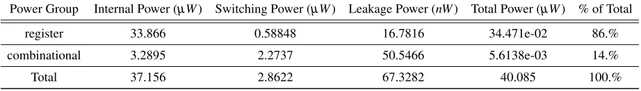
In this section, the power consumption of the 4-bit design is analyzed and outputted. For the test,
4.3 Power Consumption Analysis 19
Table 4.1: Power consumption distribution
Power Group Internal Power (µW) Switching Power (µW) Leakage Power (nW) Total Power (µW) % of Total
register 33.866 0.58848 16.7816 34.471e-02 86.%
combinational 3.2895 2.2737 50.5466 5.6138e-03 14.%
Total 37.156 2.8622 67.3282 40.085 100.%
Power consumption is one of the most important aspects when designing a system. The goal
of every design is to make the this as minimal as possible. A low power consumption will allow
batteries to last longer and will require less cooling. One of the biggest issues is leakage power
which is power not consumed by the device to perform its necessary task.
The power consumption is outlined in table4.1. The columns describe the individual powers
that are consumed. Internal power is the energy needed to control each of the components such
as registers or logic gates. Switching power is the power needed to switch a gate or register from
one state to another. Leakage power is the amount of power that is wasted by the system when
maintaining a certain value or when parts of the design is not being used. Total power is the sum
of all the powers and the % of the total is the percentage of the sum amount of power consumed
by the individual power group.
The two power groups are register and combinational which are represented in the rows.
Register stands for the registers that consume power by storing and maintaining data every
clock cycle so that it can be used in the next clock cycle. Pipelined systems use registers to
store values at each step of the pipeline so other stages are not affected. Combinationalstands
for the combinational gates that compute a value, but do not store that value. The last row is the
Total which represents the total of each column.
It is also seen that the total dynamic power usage is 40.0180µW. Ninety-three percent of that
is the cell’s internal power at 37.1558µW and 7% is the net switching power at 2.8622µW.
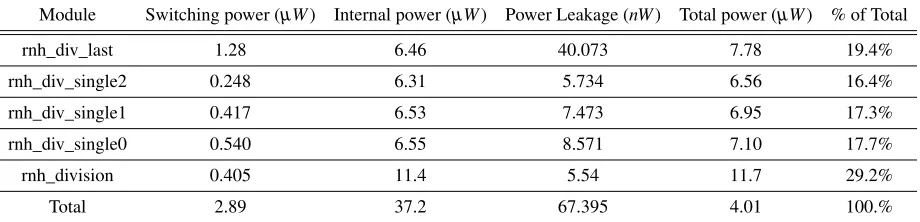
deter-4.3 Power Consumption Analysis 20
Table 4.2: Power consumption by module
Module Switching power (µW) Internal power (µW) Power Leakage (nW) Total power (µW) % of Total
rnh_div_last 1.28 6.46 40.073 7.78 19.4%
rnh_div_single2 0.248 6.31 5.734 6.56 16.4%
rnh_div_single1 0.417 6.53 7.473 6.95 17.3%
rnh_div_single0 0.540 6.55 8.571 7.10 17.7%
rnh_division 0.405 11.4 5.54 11.7 29.2%
Total 2.89 37.2 67.395 4.01 100.%
mined. This data can be found in table4.2. Similar to the previous table, the columns describe
the individual powers that are consumed.
Each row represents a different module in the design. rnh_div_last represents the last
ma-nipulation that outputs the quotient and remainder. The three modules named rnh_div_single0,
rnh_div_single1, and rnh_div_single2, are each of the single modules that compute one of the
3 steps in the 4-bit design. There are 4 steps in a 5-bit design, 5 steps in a 6-bit design, and so
on. The top-level design module is rnh_division. This module contains mostly registers and very
few combinational logic gates. The last row, the Total row, represents the total of each column.
It can be seen in the table that most of the power consumption is found in the highest level
of the design where all the values for sign, carry, dividend, and divisor for each step are stored.
The next highest is rnh_div_last which account for the final manipulation that determines the
quotient and remainder based on all other manipulations. This makes sense due to the amount of
computing that occurs during this manipulation. However, 59.5% of the power leakage is from
this module. This shows that some design changes may be needed to optimize the performance
of the last algorithm.
Using the data for the three single modules, rnh_div_single0, rnh_div_single1, and
rnh_div_single2, an equation can be derived to estimate the power usage of larger single
4.4 Area Usage Analysis 21
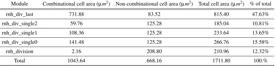
Table 4.3: Cell area by module
Module Combinational cell area (µm2) Non-combinational cell area (µm2) Total cell area (µm2) % of total
rnh_div_last 731.88 83.52 815.40 47.63%
rnh_div_single2 59.76 125.28 185.04 10.81%
rnh_div_single1 108.36 125.28 233.64 13.65%
rnh_div_single0 141.48 125.28 266.76 15.58%
rnh_division 2.16 208.80 210.96 12.32%
Total 1043.64 668.16 1711.80 100.%
the system becomes larger and approach an asymptotic value.
The logarithmic equation that is generated has an R2value of 0.9879 related to the original
data. R2is coefficient of determination that indicates the proportion of variance in the dependent
variable that is predictable from the independent variable[18]. In other words, the closer theR2
value is to 1, the closer the line is to the data. This equation can be found below.
0.4951∗ln(x) +6.5766
1000 (4.2)
4.4
Area Usage Analysis
When designing devices, cell area should be as small as possible. It costs more to manufacture
large devices at both the device level and packaging level. Also, as the components of the device
get smaller, the number of components that can be implemented in the device increases.
The overall cell area is 1711.80µm2. The module by module breakdown can be found in table
4.3. The columns are broken down into 2 major category sets and 2 conclusion data sets. The
2 major category sets arecombinationalarea andnon-combinationalarea. Non-combinational
area comes from sequential elements in the design such as registers. Combinational area comes
from the logic gates. The last two columns, total area and % of total, represent the total area for
4.4 Area Usage Analysis 22
The rows in this table are similar to the rows used in table4.2.
Unlike power consumption where the top level adds the most to the overall number,
rnh_div_last is takes up the most space. This is the last manipulation completed to output the
quotient and remainder. The combinational cell area is almost 90% of its total area, which is
understandable since there are many manipulations happening across all of the bits.
The same reasoning justifies the size of the non-combinational area of the top level design,
rnh_division. This design contains almost no logic, instead it just stores values in registers for
the entire system. It also explains why all the rnh_div_singleX designs have the same
non-combinational cell area because they all have the same amount of register outputs.
The combinational logic decreases from rnh_div_single0 down to rnh_div_single2 due to
fewer manipulations occuring. It can be seen that when more bits are being manipulated, such
as in rnh_div_single0, the area increases to the step in a logarithmic trend. Using the data, it can
be found that the increase follows the trend shown in equation4.3wherexis the number of bits
being manipulated. Similar to equation4.2, the fit will be a logarithmic trend because the cell
area will always increase with the overall size and approach an asymptote.
f(x) =73.925∗ln(x) +59.048 (4.3)
This logarithmic equation fits the original data with anR2of 0.9983.
To make a complete estimation of the total area of the single modules, an expression must
be made that includes both the combinational and non-combinational cell areas. Note that the
non-combinational area must also be added for each single manipulation. The expression for this
total cell area for the single modules can be found in equation4.4and simplified in equation4.5
4.4 Area Usage Analysis 23
register for one bit and the value 3 comes from the number of characteristic word registers.
y
∑
x=1f(x) +y∗3∗10.44∗(y−1) (4.4)
y
∑
x=1f(x) +31.32(y2−y) (4.5)
Chapter 5
Future Work
This chapter outlines how to upgrade the design to perform larger and more complex
implemen-tations. It also outlines what could possibly be upgraded or optimized to result in a better and
more efficient system.
5.1
Future and Complex Implementations
To implement the design proposed in larger and more complex systems, more components must
be added to the design.
For each bit that is added to the design, a new single manipulation module must be created.
Each new module must contain one more bit operation than the previous one. This means that
the size of the single manipulation modules will increase exponentially. The estimated sizes and
power consumption values are outlined in table 5.1 based on the data collected from the 4-bit
design using equations4.2 and4.5. A plot of the areas can be found in figure5.1 and the total
area per bit is plotted in figure5.2.
5.1 Future and Complex Implementations 25
Table 5.1: Estimated single manipulation module values
Bit width # # of Manipulations Estimated cell area (µm2) Total cell area (µm2) Estimated power usage (µW) Total power usage (µW)
4 3 140.26 685.44 7.12 20.6
5 4 161.53 1097.53 7.26 27.9
6 5 178.03 1588.76 7.37 35.3
7 6 191.50 2156.10 7.46 42.7
8 7 202.90 2797.48 7.54 50.3
16 15 259.24 10464.97 7.92 112.
32 31 312.91 38672.90 8.28 243.
64 63 365.33 144861.88 8.63 514.
[image:35.612.91.530.326.673.2]5.1 Future and Complex Implementations 26
5.1 Future and Complex Implementations 27
first column. The values 4 through 8 are given to show consecutive numbers and the bit values 16,
32, and 64 are given as the common bit widths for integer operations. The second column is the
number of manipulations that must occur before the quotient and remainder can be calculated.
This value happens to be one less than the bit width number. The third column is the estimated
combinational cell area for the largest rnh_div_singleX for the bit width. The next column is the
estimated total cell area for all the rnh_div_singleX modules combined. Estimated power usage
is the consumption from the largest rnh_div_singleX module for the given bit width. The final
column is the total power consumption of all the rnh_div_singleX modules. It is estimated that
this total power usage is about 50% of the overall total power consumption. For instance, the
overall total power consumption for a 16-bit design is estimated to be about 224µW. Similarly,
the cell area will be about 40% of the total design’s cell area leading to an estimated overall cell
area of 26000µm2for a 16-bit design.
It can be seen from the estimated data that the total area for a bit width increases
exponen-tially as expected. However, the estimated power consumption ends up being linear though it is
expected to be exponential. This may be because the estimation of the total power usage does not
include an increase for the additional bits stored in additional registers for each rnh_div_singleX
due to limitations in the original testing. This would also increase linearly due as the rise of the
bit number. This increase along to the estimated linear total power usage would combine to make
an exponential increase.
It is expected that timing should remain roughly the same when the bit width increases. This
is due to the all the modules being very close to the top level design. In other words, timing is
expected to not be the limiting factor of larger designs.
In addition to the exponential findings, upgrades must be performed on the algorithm to
ac-count for some extra states that were not designed or tested for. The extra states result when the
ex-5.2 Optimizations 28
pressions to update the dividend, carry, and sign values change. In some cases, the dividend and
carry value will also have to exceed the limitation of 2 bits, which leads to even more complexity.
Because of this, the design will work best with smaller and simpler systems.
5.2
Optimizations
The proposed system works completely and efficiently, but there are some areas for improvement.
One area for improvement is the overall system evaluating every single manipulation
mod-ule. This it isn’t necessary. The current design requires every bit to be checked for a possible
manipulation. A better design could can perform more efficiently by only checking for the most
significant 1. It could also stop checking for manipulations after the entire divisor has been
completely used. This could lead to less power consumption of the entire system and therefore
optimizing the design. The downside of this optimization is more controls would needed to be
implemented which result is higher cell area usage.
Due to the large amount of power loss from the module rnh_div_last, optimizations should
be made to limit this. Combining logic together to limit the number of logic gates that are not
used in every scenario will help bring the power loss down.
Another example of optimization is the final manipulation to solve for the quotient and
re-mainder. The final manipulation could be completed in earlier steps, resulting in the throughput
latency being one clock cycle less. However, this results in the algorithm not being straight
Chapter 6
Conclusion
A model of a 4-bit division core based on an ancient Vedic mathematics operation is successfully
designed and created. The core is modeled using Verilog and simulated using Cadence’s Incisive
Suite. The design is synthesized and analyzed using Synopsis’s DC Ultra and used to estimate
the operation larger models.
The design is successfully simulated with every possible input combination and checked for
correct operation using a generated test-bench. The test-bench is generated using Python which
allows for future test-benches to be created and implemented easily.
In timing analysis, the design has very little impact. The maximum allowable clock is found
to be about 400MHz as opposed to the 50MHz clock used to analyze the design. This means
that timing will not be a factor when implementing this design in larger models or in processors.
With a clock cycle of 400MHz, 16-clock cycles would take 40ns. This means that the worst case
for a 16-bit system would take about 40nsto compute the quotient and remainder. In comparison
to a similar design based on the same algorithm, the worst case is 3.9µs[9]. This shows current
design may end up being more efficient when considering timing. However, more research and
30
The total power consumption is 40.085µW with 67.3282nW being consumed as leakage.
It is estimated that in a 16-bit design, the total power consumption will increase exponentially
towards 224µW. After comparing this to a similar design showing only 24µW[8], it is clear that
this design needs to be reworked.
The cell area usage is 1711.80µm2. It is predicted that the area will increase exponentially
and end up being 0.026mm2 for a 16-bit design. Comparing this to 10.25mm2 in a similar
design[8], it can be seen that while power consumption is higher, the design takes up
signifi-cantly less space.
From the comparisons, it can be seen that some improvements must be made in order to
increase the ability of the design. Different components must be added to the current design to
allow for the evaluation of all the combinations of inputs into the Vedic division algorithm. In
addition, the power consumption must be minimized by modifying the design to not consume
as much power when evaluating the quotient and remainder especially in the final algorithm
implementation.
Overall, the possibility of this design to be implemented in a processor or other embedded
systems is quite high. After some optimizations and upgrading, this design could fully function in
many different sized bit systems by replacing older, slower, or less optimized division cores. The
recommendation of this graduate paper is to continue research and development of this method
References
[1] J. Squire. Cmsc 411 lecture 19, pipelining data forwarding.
[2] Kenneth Pletcher. The History of India. Britannica Educational Pub. in association with
Rosen Educational Services, 2011.
[3] Gavin D. Flood. The Blackwell companion to Hinduism. Blackwell, 2005.
[4] Pierre-Sylvain Filliozat. Ancient sanskrit mathematics: An oral tradition and a written
literature. History of Science, History of Text Boston Studies in the Philosophy of Science,
2004.
[5] Bharatikrshnatirtha and Vasudeva S. Agrawala.Vedic mathematics, or, sixteen simple
math-ematical formulae from the Vedas (for one-line answers to all mathmath-ematical problems).
Motilal Banarsidass, 1970.
[6] Lianghuo Fan. A generalization of synthetic division and a general theorem of division
polynomials. Mathematical Medley, 30(1), Jun 2003.
[7] Swami Bharati Krishna Tirtha and Vasudeva Sharana. Vedic Mathematics. Motilal
Banar-sidass Publishers Private Limited, 2004.
References 32
Novel architecture (asic) for high speed vlsi applications. 2011 International Symposium
on Electronic System Design, 2011.
[9] D. Sengupta, M. Sultana, and A. Chaudhuri. An algorithm facilitating fast bcd division
on low end processors using ancient indian vedic mathematics sutras. 2012 International
Conference on Communications, Devices and Intelligent Systems (CODIS), 2012.
[10] D. E. Thomas and Philip R. Moorby.The Verilog Hardware Description Language. Kluwer
Academic Publishers, 1991.
[11] Verilog. Introduction to Verilog, 2015.
[12] Guido van Rossum. The history of python, Jan 1970.
[13] Python. General python faq. 2017.
[14] Moshe Zadka and A M Kuchling. Whats new in python 2.0, Oct 2000.
[15] Cadence. SimVision Debug.
[16] Synopsis. DC Ultra, 2015.
[17] 32x8.com. Logic circuit simplification (sop and pos).
Appendix I
Verilog Design Code
1 module r n h _ d i v i s i o n ( r e s e t , c l k , d i v i s o r _ i n , d i v i d e n d _ i n ,
q u o t i e n t _ o u t , r e m a i n d e r _ o u t , s c a n _ i n 0 , s c a n _ e n , t e s t _ m o d e ,
s c a n _ o u t 0 ) ;
2 i n p u t
3 r e s e t , / / s y s t e m r e s e t
4 c l k ; / / s y s t e m c l o c k
5 i n p u t
6 s c a n _ i n 0 , / / t e s t s c a n mode d a t a i n p u t
7 s c a n _ e n , / / t e s t s c a n mode e n a b l e
8 t e s t _ m o d e ; / / t e s t mode s e l e c t
9 o u t p u t
10 s c a n _ o u t 0 ; / / t e s t s c a n mode d a t a o u t p u t m o d u l e
r n h _ d i v i s i o n
11
34
13
14 o u t p u t [ 3 : 0 ] q u o t i e n t _ o u t , r e m a i n d e r _ o u t ;
15 w i r e [ 3 : 0 ] d i v i s o r _ i n , d i v i d e n d _ i n ;
16
17 w i r e [ 3 : 0 ] q u o t i e n t _ o u t , r e m a i n d e r _ o u t ;
18
19 / /−−−−−−−− i n t e r n a l s i g a n l s −−−−−−−−−−−//
20 r e g [ 3 : 0 ] d i v i s o r 0 ; / / 4 4−b i t r e g i s t e r s f o r d i v i s o r
21 r e g [ 3 : 0 ] d i v i d e n d 0 ; / / 4 4−b i t r e g i s t e r s f o r d i v i d e n d
22
23 w i r e [ 3 : 0 ] d i v i d e n d _ o u t [ 3 : 0 ] ; / / 4 4−b i t w i r e s f o r
d i v i d e n d o u t p u t s
24 w i r e [ 3 : 0 ] c a r r y _ o u t [ 2 : 0 ] ;
25 w i r e [ 3 : 0 ] s i g n _ o u t [ 2 : 0 ] ;
26 r e g [ 3 : 0 ] d i v i s o r 1 , d i v i s o r 2 , d i v i s o r 3 ;
27 w i r e [ 3 : 0 ] d i v i d e n d 1 , d i v i d e n d 2 , d i v i d e n d 3 ;
28 w i r e [ 3 : 0 ] c a r r y 1 , c a r r y 2 , c a r r y 3 ;
29 w i r e [ 3 : 0 ] s i g n 1 , s i g n 2 , s i g n 3 ;
30
31 / /−−−−−−−−−−− c o n n e c t e d m o d u l e s −−−−−−−−−−−−−//
32 r n h _ d i v _ s i n g l e 0 my_div0 ( c l k , r e s e t , d i v i s o r 0 , d i v i d e n d 0 , 4 ’
b0000 , 4 ’ b0000 , d i v i d e n d 1 , c a r r y 1 , s i g n 1 ,
33 s c a n _ i n 0 , s c a n _ e n , t e s t _ m o d e , s c a n _ o u t 0 ) ;
34 r n h _ d i v _ s i n g l e 1 my_div1 ( c l k , r e s e t , d i v i s o r 1 , d i v i d e n d 1 ,
35
35 s c a n _ i n 0 , s c a n _ e n , t e s t _ m o d e , s c a n _ o u t 0 ) ;
36 r n h _ d i v _ s i n g l e 2 my_div2 ( c l k , r e s e t , d i v i s o r 2 , d i v i d e n d 2 ,
c a r r y 2 , s i g n 2 , d i v i d e n d 3 , c a r r y 3 , s i g n 3 ,
37 s c a n _ i n 0 , s c a n _ e n , t e s t _ m o d e , s c a n _ o u t 0 ) ;
38 r n h _ d i v _ l a s t m y _ l a s t ( c l k , r e s e t , d i v i s o r 3 , d i v i d e n d 3 , c a r r y 3 ,
s i g n 3 , q u o t i e n t _ o u t , r e m a i n d e r _ o u t ,
39 s c a n _ i n 0 , s c a n _ e n , t e s t _ m o d e , s c a n _ o u t 0 ) ;
40 / /−−−−−−−−− module b e g i n −−−−−−−−−−−−−−−−//
41
42 always@ (p o s e d g e c l k o r p o s e d g e r e s e t ) b e g i n
43 i f ( r e s e t == 1 ’ b1 ) b e g i n
44 d i v i s o r 0 = 4 ’ b0000 ; d i v i s o r 1 = 4 ’ b0000 ; d i v i s o r 2 = 4 ’
b0000 ; d i v i s o r 3 = 4 ’ b0000 ;
45 d i v i d e n d 0 = 4 ’ b0000 ;
46 end
47 e l s e b e g i n
48 d i v i s o r 3 = d i v i s o r 2 ;
49 d i v i s o r 2 = d i v i s o r 1 ;
50 d i v i s o r 1 = d i v i s o r 0 ;
51 d i v i s o r 0 = d i v i s o r _ i n ;
52 d i v i d e n d 0 = d i v i d e n d _ i n ;
53 end
54 end
55 e n d m o d u l e
36
57 module r n h _ d i v _ s i n g l e 0 ( c l k , r e s e t , d i v i s o r , d i v i d e n d , c a r r y ,
s i g n , d i v i d e n d _ o u t , c a r r y _ o u t , s i g n _ o u t , s c a n _ i n 0 , s c a n _ e n ,
t e s t _ m o d e , s c a n _ o u t 0 ) ;
58 i n p u t c l k , r e s e t ;
59 i n p u t [ 3 : 0 ] d i v i s o r , d i v i d e n d , c a r r y , s i g n ;
60 o u t p u t [ 3 : 0 ] d i v i d e n d _ o u t , c a r r y _ o u t , s i g n _ o u t ;
61 i n p u t
62 s c a n _ i n 0 , / / t e s t s c a n mode d a t a i n p u t
63 s c a n _ e n , / / t e s t s c a n mode e n a b l e
64 t e s t _ m o d e ; / / t e s t mode s e l e c t
65 o u t p u t
66 s c a n _ o u t 0 ; / / t e s t s c a n mode d a t a o u t p u t m o d u l e
r n h _ d i v i s i o n
67
68 w i r e [ 1 : 0 ] b i t _ n u m ;
69 w i r e [ 2 : 0 ] t e m p _ d i v ;
70
71 r e g [ 3 : 0 ] d i v i d e n d _ o u t , c a r r y _ o u t , s i g n _ o u t ;
72
73 r n h _ d i v i s o r _ d e t e c t m y _ d e t e c t ( d i v i s o r , b i t _ n u m , t e m p _ d i v ,
s c a n _ i n 0 , s c a n _ e n , t e s t _ m o d e , s c a n _ o u t 0 , r e s e t , c l k ) ;
74 always@ (p o s e d g e c l k o r p o s e d g e r e s e t ) b e g i n
75 i f ( r e s e t == 1 ’ b1 ) b e g i n
76 d i v i d e n d _ o u t = 4 ’ b0000 ;
37
78 s i g n _ o u t = 4 ’ b0000 ;
79 end
80 e l s e b e g i n
81 s i g n _ o u t = s i g n ;
82 c a r r y _ o u t = c a r r y ;
83 d i v i d e n d _ o u t = d i v i d e n d ;
84 i f ( b i t _ n u m <= 3 ) b e g i n
85 c a s e x( { c a r r y [ 3 ] , d i v i d e n d [ 3 ] , s i g n [ 3 ] } )
86 3 ’ bx11 , 3 ’ b1x1 : b e g i n
87 i f ( b i t _ n u m > 0 ) b e g i n
88 i f ( d i v i d e n d [ 3 ] == 1 ’ b1 )
89 d i v i d e n d _ o u t [ 2 ] = ( ~ ( t e m p _ d i v [ b i t _ n u m−1 ] ) & d i v i d e n d
[ 2 ] ) | ( t e m p _ d i v [ b i t _ n u m−1] & ~ ( d i v i d e n d [ 2 ] ) &
d i v i d e n d [ 3 ] ) ;
90 c a r r y _ o u t [ 2 ] = c a r r y [ 2 ] | ~ ( s i g n [ 2 ] ) &
t e m p _ d i v [ b i t _ n u m−1] & d i v i d e n d [ 2 ] | (
c a r r y [ 3 ] & t e m p _ d i v [ b i t _ n u m−1 ] ) ;
91 s i g n _ o u t [ 2 ] = ( c a r r y [ 2 ] & s i g n [ 2 ] ) | ( s i g n
[ 2 ] & ~ ( t e m p _ d i v [ b i t _ n u m−1 ] ) ) ;
92 end
93 i f ( b i t _ n u m > 1 ) b e g i n
94 i f ( d i v i d e n d [ 3 ] == 1 ’ b1 )
95 d i v i d e n d _ o u t [ 1 ] = ( ~ ( t e m p _ d i v [ b i t _ n u m−2 ] ) & d i v i d e n d
[ 1 ] ) | ( t e m p _ d i v [ b i t _ n u m−2] & ~ ( d i v i d e n d [ 1 ] ) &
38
96 c a r r y _ o u t [ 1 ] = c a r r y [ 1 ] | ~ ( s i g n [ 1 ] ) &
t e m p _ d i v [ b i t _ n u m−2] & d i v i d e n d [ 1 ] | (
c a r r y [ 2 ] & t e m p _ d i v [ b i t _ n u m−2 ] ) ;
97 s i g n _ o u t [ 1 ] = ( c a r r y [ 1 ] & s i g n [ 1 ] ) | ( s i g n
[ 1 ] & ~ ( t e m p _ d i v [ b i t _ n u m−2 ] ) ) ;
98 end
99
100 i f ( b i t _ n u m > 2 ) b e g i n
101 i f ( d i v i d e n d [ 3 ] == 1 ’ b1 )
102 d i v i d e n d _ o u t [ 0 ] = ( ~ ( t e m p _ d i v [ b i t _ n u m−3 ] ) & d i v i d e n d
[ 0 ] ) | ( t e m p _ d i v [ b i t _ n u m−3] & ~ ( d i v i d e n d [ 0 ] ) &
d i v i d e n d [ 3 ] ) ;
103 c a r r y _ o u t [ 0 ] = c a r r y [ 1 ] | ~ ( s i g n [ 0 ] ) &
t e m p _ d i v [ b i t _ n u m−3] & d i v i d e n d [ 0 ] | (
c a r r y [ 3 ] & t e m p _ d i v [ b i t _ n u m−3 ] ) ;
104 s i g n _ o u t [ 0 ] = ( c a r r y [ 0 ] & s i g n [ 0 ] ) | ( s i g n
[ 0 ] & ~ ( t e m p _ d i v [ b i t _ n u m−3 ] ) ) ;
105 end
106 end
107 3 ’ bx10 , 3 ’ b1x0 : b e g i n
108 i f ( b i t _ n u m > 0 ) b e g i n
109 i f ( d i v i d e n d [ 3 ] == 1 ’ b1 )
110 d i v i d e n d _ o u t [ 2 ] = ( ~ ( t e m p _ d i v [ b i t _ n u m−1 ] ) & d i v i d e n d
[ 2 ] ) | ( t e m p _ d i v [ b i t _ n u m−1] & ~ ( d i v i d e n d [ 2 ] ) &
39
111 c a r r y _ o u t [ 2 ] = ( c a r r y [ 2 ] & ~ t e m p _ d i v [
b i t _ n u m−1 ] ) | ( c a r r y [ 2 ] & d i v i d e n d [ 2 ] ) |
( s i g n [ 2 ] & c a r r y [ 2 ] ) |
112 ( s i g n [ 2 ] & t e m p _ d i v [ b i t _ n u m−1] & d i v i d e n d [ 2 ] ) | (
c a r r y [ 3 ] & t e m p _ d i v [ b i t _ n u m−1 ] ) ;
113 s i g n _ o u t [ 2 ] = s i g n [ 2 ] | ( ~ c a r r y [ 2 ] &
t e m p _ d i v [ b i t _ n u m−1] & ~ d i v i d e n d [ 2 ] ) ;
114 end
115 i f ( b i t _ n u m > 1 ) b e g i n
116 i f ( d i v i d e n d [ 3 ] == 1 ’ b1 )
117 d i v i d e n d _ o u t [ 1 ] = ( ~ ( t e m p _ d i v [ b i t _ n u m−2 ] ) & d i v i d e n d
[ 1 ] ) | ( t e m p _ d i v [ b i t _ n u m−2] & ~ ( d i v i d e n d [ 1 ] ) &
d i v i d e n d [ 3 ] ) ;
118 c a r r y _ o u t [ 1 ] = ( c a r r y [ 1 ] & ~ t e m p _ d i v [
b i t _ n u m−2 ] ) | ( c a r r y [ 1 ] & d i v i d e n d [ 1 ] ) |
( s i g n [ 1 ] & c a r r y [ 1 ] ) |
119 ( s i g n [ 1 ] & t e m p _ d i v [ b i t _ n u m−2] & d i v i d e n d [ 1 ] ) | (
c a r r y [ 3 ] & t e m p _ d i v [ b i t _ n u m−2 ] ) ;
120 s i g n _ o u t [ 1 ] = s i g n [ 1 ] | ( ~ c a r r y [ 1 ] &
t e m p _ d i v [ b i t _ n u m−2] & ~ d i v i d e n d [ 1 ] ) ;
121 end
122 i f ( b i t _ n u m > 2 ) b e g i n
123 i f ( d i v i d e n d [ 3 ] == 1 ’ b1 )
124 d i v i d e n d _ o u t [ 0 ] = ( ~ ( t e m p _ d i v [ b i t _ n u m−3 ] ) & d i v i d e n d
40
d i v i d e n d [ 3 ] ) ;
125 c a r r y _ o u t [ 0 ] = ( c a r r y [ 0 ] & ~ t e m p _ d i v [
b i t _ n u m−3 ] ) | ( c a r r y [ 0 ] & d i v i d e n d [ 0 ] ) |
( s i g n [ 0 ] & c a r r y [ 0 ] ) |
126 ( s i g n [ 0 ] & t e m p _ d i v [ b i t _ n u m−3] & d i v i d e n d [ 0 ] ) | (
c a r r y [ 3 ] & t e m p _ d i v [ b i t _ n u m−3 ] ) ;
127 s i g n _ o u t [ 0 ] = s i g n [ 0 ] | ( ~ c a r r y [ 0 ] &
t e m p _ d i v [ b i t _ n u m−3] & ~ d i v i d e n d [ 0 ] ) ;
128 end
129 end
130 d e f a u l t : b e g i n
131 d i v i d e n d _ o u t [ 2 : 0 ] = d i v i d e n d [ 2 : 0 ] ;
132 s i g n _ o u t = s i g n ;
133 c a r r y _ o u t = c a r r y ;
134 end
135 e n d c a s e
136 d i v i d e n d _ o u t [ 3 ] = d i v i d e n d [ 3 ] ;
137 end
138 end
139 end
140 e n d m o d u l e
141 module r n h _ d i v _ s i n g l e 1 ( c l k , r e s e t , d i v i s o r , d i v i d e n d , c a r r y ,
s i g n , d i v i d e n d _ o u t , c a r r y _ o u t , s i g n _ o u t , s c a n _ i n 0 , s c a n _ e n ,
t e s t _ m o d e , s c a n _ o u t 0 ) ;
41
143 i n p u t [ 3 : 0 ] d i v i s o r , d i v i d e n d , c a r r y , s i g n ;
144 o u t p u t [ 3 : 0 ] d i v i d e n d _ o u t , c a r r y _ o u t , s i g n _ o u t ;
145 i n p u t
146 s c a n _ i n 0 , / / t e s t s c a n mode d a t a i n p u t
147 s c a n _ e n , / / t e s t s c a n mode e n a b l e
148 t e s t _ m o d e ; / / t e s t mode s e l e c t
149 o u t p u t
150 s c a n _ o u t 0 ; / / t e s t s c a n mode d a t a
o u t p u t m o d u l e r n h _ d i v i s i o n
151
152 w i r e [ 1 : 0 ] b i t _ n u m ;
153 w i r e [ 2 : 0 ] t e m p _ d i v ;
154
155 r e g [ 3 : 0 ] d i v i d e n d _ o u t , c a r r y _ o u t , s i g n _ o u t ;
156
157 r n h _ d i v i s o r _ d e t e c t m y _ d e t e c t ( d i v i s o r , b i t _ n u m , t e m p _ d i v ,
s c a n _ i n 0 , s c a n _ e n , t e s t _ m o d e , s c a n _ o u t 0 , r e s e t , c l k ) ;
158 always@ (p o s e d g e c l k o r p o s e d g e r e s e t ) b e g i n
159 i f ( r e s e t == 1 ’ b1 ) b e g i n
160 d i v i d e n d _ o u t = 4 ’ b0000 ;
161 c a r r y _ o u t = 4 ’ b0000 ;
162 s i g n _ o u t = 4 ’ b0000 ;
163 end
164 e l s e b e g i n
42
166 c a r r y _ o u t = c a r r y ;
167 d i v i d e n d _ o u t = d i v i d e n d ;
168 i f ( b i t _ n u m <= 2 ) b e g i n
169 c a s e x( { c a r r y [ 2 ] , d i v i d e n d [ 2 ] , s i g n [ 2 ] } )
170 3 ’ bx11 , 3 ’ b1x1 : b e g i n
171 i f ( b i t _ n u m > 0 ) b e g i n
172 i f ( d i v i d e n d [ 2 ] == 1 ’ b1 )
173 d i v i d e n d _ o u t [ 1 ] = ( ~ t e m p _ d i v [ b i t _ n u m−1] & d i v i d e n d
[ 1 ] ) | ( t e m p _ d i v [ b i t _ n u m−1] & ~ d i v i d e n d [ 1 ] &
d i v i d e n d [ 2 ] ) ;
174 c a r r y _ o u t [ 1 ] = c a r r y [ 1 ] | ~ ( s i g n [ 1 ] ) &
t e m p _ d i v [ b i t _ n u m−1] & d i v i d e n d [ 1 ] | (
c a r r y [ 2 ] & t e m p _ d i v [ b i t _ n u m−1 ] ) ;
175 s i g n _ o u t [ 1 ] = ( s i g n [ 1 ] & ~ ( t e m p _ d i v [ b i t _ n u m
−1 ] ) ) | ( s i g n [ 1 ] & c a r r y [ 1 ] ) ;
176 end
177
178 i f ( b i t _ n u m > 1 ) b e g i n
179 i f ( d i v i d e n d [ 2 ] == 1 ’ b1 )
180 d i v i d e n d _ o u t [ 0 ] = ( ~ t e m p _ d i v [ b i t _ n u m−2] & d i v i d e n d
[ 0 ] ) | ( t e m p _ d i v [ b i t _ n u m−2] & ~ d i v i d e n d [ 0 ] &
d i v i d e n d [ 2 ] ) ;
181 c a r r y _ o u t [ 0 ] = c a r r y [ 0 ] | ~ ( s i g n [ 0 ] ) &
t e m p _ d i v [ b i t _ n u m−2] & d i v i d e n d [ 0 ] | (
43
182 s i g n _ o u t [ 0 ] = ( s i g n [ 0 ] & ~ ( t e m p _ d i v [ b i t _ n u m
−2 ] ) ) + ( s i g n [ 0 ] & c a r r y [ 0 ] ) ;
183 end
184 end
185 3 ’ bx10 , 3 ’ b1x0 : b e g i n
186 i f ( b i t _ n u m > 0 ) b e g i n
187 i f ( d i v i d e n d [ 2 ] == 1 ’ b1 )
188 d i v i d e n d _ o u t [ 1 ] = ( ~ ( t e m p _ d i v [ b i t _ n u m−1 ] ) & d i v i d e n d
[ 1 ] ) | ( t e m p _ d i v [ b i t _ n u m−1] & ~ ( d i v i d e n d [ 1 ] ) &
d i v i d e n d [ 2 ] ) ;
189 c a r r y _ o u t [ 1 ] = ( c a r r y [ 1 ] & ~ t e m p _ d i v [
b i t _ n u m−1 ] ) | ( c a r r y [ 1 ] & d i v i d e n d [ 1 ] ) |
( s i g n [ 1 ] & c a r r y [ 1 ] ) |
190 ( s i g n [ 1 ] & t e m p _ d i v [ b i t _ n u m−1] & d i v i d e n d [ 1 ] ) | (
c a r r y [ 2 ] & t e m p _ d i v [ b i t _ n u m−1 ] ) ;
191 s i g n _ o u t [ 1 ] = s i g n [ 1 ] | ( ~ c a r r y [ 1 ] &
t e m p _ d i v [ b i t _ n u m−1] & ~ d i v i d e n d [ 1 ] ) ;
192 end
193 i f ( b i t _ n u m > 1 ) b e g i n
194 i f ( d i v i d e n d [ 2 ] == 1 ’ b1 )
195 d i v i d e n d _ o u t [ 0 ] = ( ~ ( t e m p _ d i v [ b i t _ n u m−2 ] ) & d i v i d e n d
[ 0 ] ) | ( t e m p _ d i v [ b i t _ n u m−2] & ~ ( d i v i d e n d [ 0 ] ) &
d i v i d e n d [ 2 ] ) ;
196 c a r r y _ o u t [ 0 ] = ( c a r r y [ 0 ] & ~ t e m p _ d i v [
44
( s i g n [ 0 ] & c a r r y [ 0 ] ) |
197 ( s i g n [ 0 ] & t e m p _ d i v [ b i t _ n u m−2] & d i v i d e n d [ 0 ] ) | (
c a r r y [ 2 ] & t e m p _ d i v [ b i t _ n u m−2 ] ) ;
198 s i g n _ o u t [ 0 ] = s i g n [ 0 ] | ( ~ c a r r y [ 0 ] &
t e m p _ d i v [ b i t _ n u m−2] & ~ d i v i d e n d [ 0 ] ) ;
199 end
200 end
201 d e f a u l t : b e g i n
202 d i v i d e n d _ o u t [ 1 : 0 ] = d i v i d e n d [ 1 : 0 ] ;
203 s i g n _ o u t = s i g n ;
204 c a r r y _ o u t = c a r r y ;
205 end
206 e n d c a s e
207 end
208 end
209 end
210 e n d m o d u l e
211 module r n h _ d i v _ s i n g l e 2 ( c l k , r e s e t , d i v i s o r , d i v i d e n d , c a r r y ,
s i g n , d i v i d e n d _ o u t , c a r r y _ o u t , s i g n _ o u t , s c a n _ i n 0 , s c a n _ e n ,
t e s t _ m o d e , s c a n _ o u t 0 ) ;
212 i n p u t c l k , r e s e t ;
213 i n p u t [ 3 : 0 ] d i v i s o r , d i v i d e n d , c a r r y , s i g n ;
214 o u t p u t [ 3 : 0 ] d i v i d e n d _ o u t , c a r r y _ o u t , s i g n _ o u t ;
215 i n p u t
45
217 s c a n _ e n , / / t e s t s c a n mode e n a b l e
218 t e s t _ m o d e ; / / t e s t mode s e l e c t
219 o u t p u t
220 s c a n _ o u t 0 ; / / t e s t s c a n mode d a t a o u t p u t m o d u l e
r n h _ d i v i s i o n
221
222 w i r e [ 1 : 0 ] b i t _ n u m ;
223 w i r e [ 2 : 0 ] t e m p _ d i v ;
224
225 r e g [ 3 : 0 ] d i v i d e n d _ o u t , c a r r y _ o u t , s i g n _ o u t ;
226
227 r n h _ d i v i s o r _ d e t e c t m y _ d e t e c t ( d i v i s o r , b i t _ n u m , t e m p _ d i v ,
s c a n _ i n 0 , s c a n _ e n , t e s t _ m o d e , s c a n _ o u t 0 , r e s e t , c l k ) ;
228 always@ (p o s e d g e c l k o r p o s e d g e r e s e t ) b e g i n
229 i f ( r e s e t == 1 ’ b1 ) b e g i n
230 d i v i d e n d _ o u t = 4 ’ b0000 ;
231 c a r r y _ o u t = 4 ’ b0000 ;
232 s i g n _ o u t = 4 ’ b0000 ;
233 end
234 e l s e b e g i n
235 s i g n _ o u t = s i g n ;
236 c a r r y _ o u t = c a r r y ;
237 d i v i d e n d _ o u t = d i v i d e n d ;
238 i f ( b i t _ n u m <= 1 ) b e g i n
46
240 3 ’ bx11 , 3 ’ b1x1 : b e g i n
241 i f ( b i t _ n u m > 0 ) b e g i n
242 i f ( d i v i d e n d [ 1 ] == 1 ’ b1 | ( s i g n [ 0 ] == 1 ’ b1
& d i v i d e n d [ 0 ] == 1 ’ b1 ) )
243 d i v i d e n d _ o u t [ 0 ] = ( ~ ( t e m p _ d i v [ b i t _ n u m−1 ] ) & d i v i d e n d
[ 0 ] ) | ( t e m p _ d i v [ b i t _ n u m−1] & ~ ( d i v i d e n d [ 0 ] ) ) |
244 ( d i v i d e n d [ 0 ] & t e m p _ d i v [ b i t _ n u m−1] & c a r r y [ 1 ] ) ;
245 c a r r y _ o u t [ 0 ] = c a r r y [ 0 ] | ~ ( s i g n [ 0 ] ) &
t e m p _ d i v [ b i t _ n u m−1] & d i v i d e n d [ 0 ] | (
c a r r y [ 1 ] & t e m p _ d i v [ b i t _ n u m−1 ] ) ;
246 s i g n _ o u t [ 0 ] = ( s i g n [ 0 ] & ~ ( t e m p _ d i v [ b i t _ n u m
−1 ] ) ) | ( s i g n [ 0 ] & c a r r y [ 0 ] ) ;
247 end
248 end
249 3 ’ bx10 , 3 ’ b1x0 : b e g i n
250 i f ( b i t _ n u m > 0 ) b e g i n
251 i f ( d i v i d e n d [ 1 ] == 1 ’ b1 | ( s i g n [ 0 ] == 1 ’ b0
& d i v i d e n d [ 0 ] == 1 ’ b1 ) )
252 d i v i d e n d _ o u t [ 0 ] = ( ~ ( t e m p _ d i v [ b i t _ n u m−1 ] ) & d i v i d e n d
[ 0 ] ) | ( t e m p _ d i v [ b i t _ n u m−1] & ~ ( d i v i d e n d [ 0 ] ) ) |
253 ( d i v i d e n d [ 0 ] & t e m p _ d i v [ b i t _ n u m−1] & c a r r y [ 1 ] ) ;
254 c a r r y _ o u t [ 0 ] = ( c a r r y [ 0 ] & ~ t e m p _ d i v [
b i t _ n u m−1 ] ) | ( c a r r y [ 0 ] & d i v i d e n d [ 0 ] ) |
47
255 ( s i g n [ 0 ] & t e m p _ d i v [ b i t _ n u m−1] & d i v i d e n d [ 0 ] ) | (
c a r r y [ 1 ] & t e m p _ d i v [ b i t _ n u m−1] & ~ d i v i d e n d [ 0 ] ) ;
256 s i g n _ o u t [ 0 ] = s i g n [ 0 ] | ( ~ c a r r y [ 0 ] &
t e m p _ d i v [ b i t _ n u m−1] & ~ d i v i d e n d [ 0 ] ) | (
c a r r y [ 1 ] ) ;
257 end
258 end
259 d e f a u l t : b e g i n
260 d i v i d e n d _ o u t [ 0 ] = d i v i d e n d [ 0 ] ;
261 s i g n _ o u t = s i g n ;
262 c a r r y _ o u t = c a r r y ;
263 end
264 e n d c a s e
265 end
266 end
267 end
268 e n d m o d u l e
269
270 module r n h _ d i v _ l a s t ( c l k , r e s e t , d i v i s o r , d i v i d e n d , c a r r y , s i g n
, q u o t i e n t _ o u t , r e m a i n d e r _ o u t , s c a n _ i n 0 , s c a n _ e n , t e s t _ m o d e ,
s c a n _ o u t 0 ) ;
271 i n p u t c l k , r e s e t ;
272 i n p u t [ 3 : 0 ] d i v i s o r , d i v i d e n d , c a r r y , s i g n ;
273 o u t p u t [ 3 : 0 ] q u o t i e n t _ o u t , r e m a i n d e r _ o u t ;
48
275 s c a n _ i n 0 , / / t e s t s c a n mode d a t a i n p u t
276 s c a n _ e n , / / t e s t s c a n mode e n a b l e
277 t e s t _ m o d e ; / / t e s t mode s e l e c t
278 o u t p u t
279 s c a n _ o u t 0 ; / / t e s t s c a n mode d a t a o u t p u t m o d u l e
r n h _ d i v i s i o n
280 r e g [ 3 : 0 ] q u o t i e n t _ o u t , r e m a i n d e r _ o u t ;
281 w i r e [ 1 : 0 ] b i t _ n u m ;
282 w i r e [ 2 : 0 ] t e m p _ d i v ;
283 w i r e [ 1 : 0 ] rem_num ;
284
285 r n h _ d i v i s o r _ d e t e c t m y _ d e t e c t ( d i v i s o r , b i t _ n u m , t e m p _ d i v ,
s c a n _ i n 0 , s c a n _ e n , t e s t _ m o d e , s c a n _ o u t 0 , r e s e t , c l k ) ;
286 r n h _ r e m a i n d e r _ d e t e c t m y _ r d e t e c t ( d i v i d e n d , b i t _ n u m , rem_num ,
s c a n _ i n 0 , s c a n _ e n , t e s t _ m o d e , s c a n _ o u t 0 , r e s e t , c l k ) ;
287 always@ (p o s e d g e c l k o r p o s e d g e r e s e t ) b e g i n
288 i f ( r e s e t == 1 ’ b1 ) b e g i n
289 q u o t i e n t _ o u t = 4 ’ h0 ;
290 r e m a i n d e r _ o u t = 4 ’ h0 ;
291 end
292 e l s e b e g i n
293 c a s e( b i t _ n u m )
294 3 : b e g i n
49
296 r e m a i n d e r _ o u t = d i v i s o r [ 3 : 0 ] − { 1 ’ b0 , ( ( 3 ’ b111
& d i v i d e n d [ 2 : 0 ] & ( s i g n [ 2 : 0 ] ) ) − { ( ~ ( s i g n
[ 2 : 0 ] ) & c a r r y [ 2 : 0 ] ) −
297 ( s i g n [ 2 : 0 ] & c a r r y [ 2 : 0 ] ) , 1 ’ b0 } ) }
298 + ( d i v i d e n d [ 2 : 0 ] & ~ s i g n [ 2 : 0 ] ) ;
299 q u o t i e n t _ o u t = ( 1 ’ b1 & d i v i d e n d [ 3 ] & ~ ( s i g n [ 3 ] ) ) +
{ ( ~ ( s i g n [ 2 ] ) & c a r r y [ 2 ] ) − ( s i g n [ 2 ] & c a r r y [ 2 ] ) , 1 ’
b0 }
300 − d i v i d e n d [ rem_num ] �