promoting access to White Rose research papers
White Rose Research Online [email protected]
Universities of Leeds, Sheffield and York
http://eprints.whiterose.ac.uk/
This is the Author's Accepted version of an article published in the Journal of Applied Physics
White Rose Research Online URL for this paper:
http://eprints.whiterose.ac.uk/id/eprint/78158
Published article:
Pilgrim, NJ, Ikonic, Z and Kelsall, RW (2013) Influence of absorber layer dopants on performance of Ge/Si single photon avalanche diodes.Journal of Applied Physics, 113 (14). 144508. ISSN 0021-8979
Influence of absorber layer dopants on performance of Ge/Si Single Photon
Avalanche Diodes
Neil J. Pilgrim,1,a) Zoran Ikonic,1 and Robert W. Kelsall1
Institute of Microwaves & Photonics, University of Leeds, Leeds,
UK
Monte Carlo electronic transport simulations are applied to investigate the influence
of the Ge absorber layer on the performance of Ge/Si single photon avalanche diodes
(SPADs). Ge dopant type and concentration control the internal electric field
gradi-ents, which directly influence the probabilistic distribution of times from the point
of charge photo-generation to that of transmission over the Ge/Si heterojunction.
The electric field adjacent to the heterointerface is found to be the dominant factor
in achieving rapid transmission, leading to a preference for p-type dopants in the
Ge absorber. The contribution to jitter from the Ge layer is estimated and appears
relatively independent of bias, though scales near-linearly with layer height.
Keywords: SPAD, silicon, germanium, doping, dopants, jitter, Monte Carlo
I. INTRODUCTION
Detection of very low amplitude optical signals down to the single-photon regime is
becoming of increasing interest1, with application areas including quantum computing
and cryptography2,3, biophotonics4, laser ranging and imaging5 and semiconductor circuit
diagnostics6. One approach for measuring such signals involves adapting an avalanche
pho-todiode (APD) device and operating it in a Geiger (trigger-reset) mode, the resulting device
being commonly known as a single-photon avalanche diode (SPAD)7. SPADs have been
developed from a range of different semiconductor materials, with the most successful being
developed either from solely Si7 or from a heterostructure comprising III-V semiconductors
such as InGaAs/InP8. The former have benefited hugely from existing manufacturing
in-frastructure, and integration opportunities have led to the fabrication of arrays of SPADs
alongside CMOS logic9. However, as is well known, Si suffers from poor optical
absorp-tion properties, a negative impact which is particularly noticeable in detecabsorp-tion efficiences
at longer wavelengths towards the near infrared. On the contrary, III-V semiconductor
SPADs are far more capable when working within this spectral region, and the variety of
heterostructure designs which are possible enables device optimisation to achieve low-noise
absorption at longer wavelengths coupled with efficient multiplication.
Inspired by the added flexibility afforded by the inclusion of Ge or SiGe alloys into CMOS,
the area of silicon photonics has undergone significant recent development, with the narrower
band-gap Ge providing scope for significant improvements in optical absorption compared
to pure Si devices, particularly around the two main telecommunications wavelengths of
1.3µm and 1.55µm. This capability has led to the development of various long-wavelength photodetectors, including Ge/Si APDs in both nanoscale10 and traditional11 architectures.
We select the latter device architecture for operation as a SPAD, due to its similarity to III-V
heterostructure SPAD designs, where band-to-band tunnelling is minimised by maintaining
the electric field at a low level in the narrow band-gap absorption material. This is expected
to avoid the problems found previously when operating pure Ge APDs in Geiger mode12,13,
where 77 K operation was necessary in order to limit dark counts, but which also lowered the
maximum wavelength detected to less than 1.5µm. This design approach is supported by epitaxial techniques which allow the growth of Ge directly on Si with only a small residual
The aim of this work is to explore Ge/Si structures which might be suitable for operation
as SPADs, through the application of a Monte Carlo transport model to simulate the device
dynamics, considering which design parameters are likely to lead to designs with the highest
performance. We specifically focus on the Ge absorption layer, due to the potential impact
of unintentional dopants on device efficiency.
II. SPAD DESIGN & MODELLING APPROACH
Following an absorption event in the Ge layer, an avalanche in a Si layer might be triggered
by either one of the photogenerated carriers. However, based on the asymmetry in the
impact ionization coefficients within Si16, our analysis has initially focused upon triggering
avalanches via electrons. To achieve the appropriate orientation of electric fields (under
reverse biasing) requires an overall p-i-n design, with a p+ top Ge contact layer and an
n+ Si bottom contact layer. In order to optimize the electric fields within each material
a separate absorption, charge and multiplication (SACM or SAM) layer scheme may be
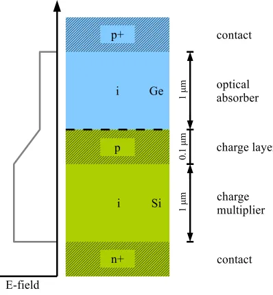
followed, resulting in a p+-i-p-i-n+ doping profile within the epitaxial layers, as illustrated
schematically in figure 1.
There are two key elements to consider when examining the performance of SPAD devices.
The first is the non-optical source of measured events, the dark count rate (DCR), which
must be maintained as low as possible. The origin of the DCR is typically a balance between
band-to-band tunnelling (at high electric fields), defect-assisted tunnelling (at high defect
densities) and generation-recombination mechanisms (at high temperature)17. Only the
first of these may be controlled through device design and would be most significant in the
narrow band-gap Ge absorption layer. The second element is the need for a sufficiently high
photon detection efficiency (PDE): the quantum efficiency must be sufficiently great so as to
produce an electron-hole pair from an incident photon, and the device must then efficiently
convert that charge into a measurable current pulse. Factors contributing to the PDE may
be subdivided according to the route the signal takes through the device: initial charge
generation, charge transport to the point of impact-ionization, and sustained avalanche to
the point where the current may be measured. The transport in the Ge layer connecting the
charge generation and avalanche processes is potentially a significant bottleneck due to the
FIG. 1. Schematic diagram of an idealised p+-i-p-i-n+ device and the corresponding electric field
profile; real devices have finite unintentional doping in the regions marked as intrinsic.
have elected to focus our analysis upon the Ge absorption layer, considering the time from
charge generation to entry of that charge into the Si charge layer.
The charge transport model chosen follows an established Monte Carlo approach18, our
implementation of which we have developed and applied over a number of years19–22 and
now extended to Ge. Since the SPAD operates in a heavily reverse-biased mode and is
essentially depleted of mobile charge except during avalanche, only electron transport is
included because the device relies upon these carriers for avalanche triggering in the Si
ellipsoidal energy surfaces around the L and ∆ symmetry locations. Parameters for the bandstructure and many of the carrier-phonon scattering processes are taken from a fit to
transport measurements23. One exception is made for the scattering deformation potentials
between the Γ and other minima, for which fits to transport measurements do not provide a
highly constrained range of values; instead values from optical measurements are used24. The
energy offsets between the valley minima incorporate the small residual strain (≈ 0.18 %) from growth of Ge on Si15, causing a small energy splitting of the ∆ minima into the ∆2 pair
and ∆4 quadruplet and other small energy shifts25,26. Simulations are performed assuming
an ambient temperature of 300 K.
In addition to the use of the Monte Carlo method for transport, a random sampling
approach is also used to account for the random locations of charge generation within the
Ge layer. Light of a given single wavelength is assumed to impinge upon the top surface of the
Ge, with a decaying probability of generation over the depth of the layer based on the
Beer-Lambert expression. The absorption coefficient is taken for Ge with the small residual strain
from after-growth cooling as indicated above27, which for an incident wavelength of 1.55µm results in a spatial distribution of carriers which is relatively homogeneous. To simplify the
collection of statistics a large ensemble of generated electrons (up to 500,000) is simulated
synchronously, enabling probability distribution data to be easily collected as a function
of time. The ensemble is generated with a thermal distribution within the Γ minimum,
representing the dominance of direct absorption and neglecting any excess photon energy
above the direct band gap.
As noted above, since the device may be considered to have a negligible amount of mobile
charge present during the simulated period (prior to significant sustained avalanching), then
a simple non-self-consistent fixed electric field profile is sufficient. The Monte Carlo transport
algorithm is then applied to the large ensemble of particles representing the electrons, in
timesteps of 1 fs, until all particles exit the simulation or a very long simulation time has
elapsed (typically 2 ns).
Particles may exit from the simulation upon reaching the top or bottom of the simulated
Ge absorption layer, primarily the latter at the heterointerface due to the electric fields
in the simulation domain. This interface behaves similarly to a non-injecting Schottky
contact in a typical Monte Carlo transport simulation28. However, it also incorporates the
reflecting) incident particles based on their momentum upon reaching the interface. The
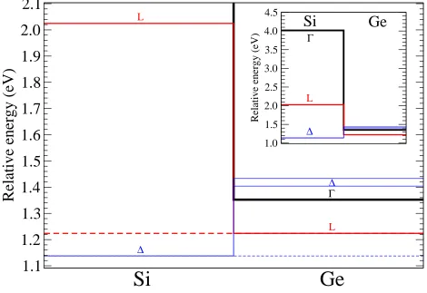
potential barriers experienced by an electron in the Ge L or Γ minima are determined through application of a theoretical value for the Si-Ge average valence band energy offset
of 0.47 eV29, in combination with the established unstrained Si band offsets at 300 K.
The transmission across the heterointerface is primarily determined according to the
rel-ative energy of the incident electron and any energy barrier for the valley within which the
electron resides at that moment, in the standard semiclassical manner. In addition, two
tun-nelling mechanisms have been examined: direct tuntun-nelling and phonon-assisted tuntun-nelling.
Direct tunnelling was calculated through application of WKB theory and a triangular
ap-proximation to the barrier shape, with barrier height determined dynamically in each case
based on a comparison of the energy of the impinging electron with the heterojunction
conduction-band energy offset. Phonon-assisted tunnelling was considered by calculating a
probability according to the dwell time in the barrier multiplied by an appropriate intervalley
scattering. The dwell time in the barrier was determined numerically30, using an approach
which is consistent with the WKB result for the triangular barrier tunnelling probability.
The scattering rate was determined in an analogous way to regular intervalley scattering
within a single material, but with one of the energy levels (minima) involved being taken
from the other material. The transitions considered were those close in energy to one
an-other: transitions in Ge from Γ andL valley states into lower-lying states corresponding to the Si ∆ valleys, and transitions in Si from upper-lying states corresponding to the Ge Γ
and L valleys into the real Si ∆ valley states. The latter correspond to electronic states in Ge extending into the Si layer, from which scattering is then possible into the real ∆ states;
the former corresponds to scattering from real states within Ge into the evanescent tail of
the Si ∆ states.
III. RESULTS
The absolute applied external bias is not important when modelling only the Ge
absorp-tion layer, since potential drops occur across other device layers according to their doping
density profiles. Consequently, rather than considering application of specific external
bi-ases, instead various electric field profiles within the Ge absorption layer (perpendicular to
1.1
1.2
1.3
1.4
1.5
1.6
1.7
1.8
1.9
2.0
2.1
Relative energy (eV)
1.0 1.5 2.0 2.5 3.0 3.5 4.0 4.5
Relative energy (eV)
[image:8.612.70.540.75.398.2]Γ L ∆
Si
Ge
Si
Ge
∆ L L ∆ ΓFIG. 2. Relative conduction-band offsets between Si and lightly-strained Ge in the flat-band case,
highlighting the potential barriers for electrons traversing from Ge into Si in theL or Γ minima. Solid lines indicate real states, dashed lines correspond to energies relevant for phonon-assisted
tunnelling (Land ∆ states only). Inset: full range of real energy minima modelled.
A. Just-active absorption layer
At low applied biases the transfer of electrons photo-generated in the Ge layer across
the heterointerface into the Si multiplication layer is severely impeded. If the background
doping is p-type, this occurs since the Ge layer is not fully depleted, causing transport to the
heterointerface to rely upon slow diffusion; if the background doping is n-type, the electric
field near the interface opposes transport in this region. As the bias is raised, an increasing
depth of the Ge absorption layer becomes active - namely having a finite electric field and
able to drift photogenerated electrons in the direction of the heterointerface. The first
operating point we consider is at the bias where the entire Ge absorption layer isjust active;
effects due to the Ge contact homojunction, the electric field profile runs from zero at one
end of the layer to a finite value at the other, the latter determined by the intervening net
background doping. The background doping is assumed to be uniform, of p- or n-type, and
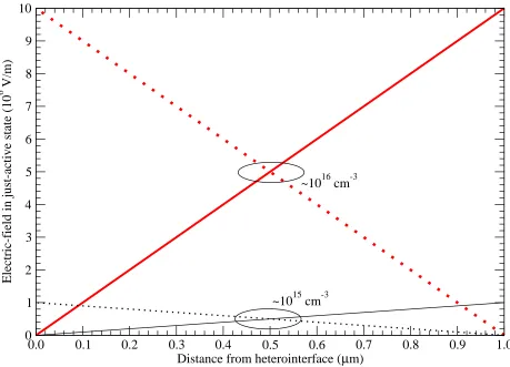
fully ionized, with densities of approximately 1015cm−3 to 1016cm−3. At the bias where the Ge layer is just active, the electric field in the Ge layer is easily calculated from electrostatics
to be given by
∆E = 1.13×10⁻⁹N L (1)
where ∆E is the shift in electric field over the height L of Ge layer, with a doping N. Substituting in a layer height of 1.0µm and the above doping density range gives peak electric fields of 1.13×10⁶V m−1 to 1.13×10⁷V m−1. Simulations have been performed with electric field profiles which vary linearly by 106V m−1 to 107V m−1 over 1µm and are shown in figure 3.
Figure 4 shows the temporal characteristics when the absorption layer is just active,
obtained by tracking the probability that a given fraction of the original ensemble of electrons
remains in the Ge layer as a function of time. Four lines are shown, for n-type (solid) and
p-type (dotted) background doping in the Ge absorber layer, each with densities of 1015cm−3 and 1016cm−3. Ideally these lines should drop to zero as rapidly as possible, indicating that electrons photo-generated in the Ge layer are rapidly and efficiently emptied into the Si
layer, such that avalanche multiplication can occur as rapidly as possible. In addition to
being directly relevant to the speed of the device, if electrons do not rapidly exit into the Si
layer then they are more likely to be affected by undesirable mechanisms in the Ge, such as
trapping and recombination.
It is clear from the figure that electrons will spend markedly less time in a p-type Ge
layer than an n-type Ge layer, and that for each type of doping, a higher doping density also
reduces the time spent in the Ge layer. The latter point is clearly related to the enhanced
energy transfer to the electrons from the higher electric field over the entire thickness of the
Ge layer, leading to a higher probability that upon reaching the heterointerface an electron
will either be in a ∆ state (with no energy barrier), or else be in anLstate and have sufficient energy to transfer over the potential barrier. The only change in the electric field profile
between p-type and n-type doping in the just-active case is as depicted in figure 3, with
the p-type profile having the highest electric field near the heterointerface and being zero at
0.0 0.1 0.2 0.3 0.4 0.5 0.6 0.7 0.8 0.9 1.0
Distance from heterointerface (µm)
0 1 2 3 4 5 6 7 8 9 10
Electric-field in just-active state (10
6 V/m)
~1016 cm-3
[image:10.612.76.535.70.401.2]~1015 cm-3
FIG. 3. Electric field profiles within the Ge absorber layer as a function of the distance from the
Ge/Si heterointerface, for p-type (dotted) and n-type (solid) doping of 1015cm−3 (thin/black lines)
and 1016cm−3 (thick/red lines), when the layer is just-active.
the improvement in transit-time characteristics associated with switching to p-type dopants
may be related to the electric field being at its peak close to the interface rather than at the
top of the device. For an n-type Ge layer, the high electric field transfers more energy to
the electrons the further they are from the heterointerface - yet when far from the interface
they have a greater distance in which to lose that energy to the lattice. For p-type Ge the
situation is reversed and improved, since the largest energy input to the electrons takes place
near the interface, where the electrons will (if they transfer over sufficiently quickly) spend
little time and stand little chance of being cooled by the lattice.
This explanation is supported by figure 5, which shows the energy dissipated to the lattice
(by sampling the net phonon emission19) over the course of each of the simulations shown
dissipa-10 p 100 p 1 n Time elapsed after charge generation (s)
0.0 0.1 0.2 0.3 0.4 0.5 0.6 0.7 0.8 0.9 1.0
Probability of electron remaining in Ge layer
thin/black: ~1015 cm-3
thick/red: ~1016 cm-3
n-type Ge
p-type Ge
[image:11.612.73.539.72.411.2]Ge doping density
FIG. 4. Probability of a photo-generated electron remaining in a just-active Ge absorption layer as
a function of time, characterising the transmission over the Ge/Si heterointerface. Doping type and
density combinations are as in figure 3: p-type (dotted) and n-type (solid); 1015cm−3 (thin/black
lines) and 1016cm−3 (thick/red lines).
tion towards the interface, in line with the increasing electric field and also the aggregate
contribution arising from increasing numbers of electrons which pass through locations close
to the interface. For n-type doping, maximum dissipation occurs in the centre of the Ge
absorption layer. While this distribution of energy dissipation within the Ge absorption
layer should not influence the transport characteristics in the case of single photon
opera-tion, it is interesting to compare the curves in figure 5 and 4. The inefficiencies of n-type
doping are emphasised through comparison of the highly-doped (thick/red) n-type (solid)
and p-type (dotted) results in these two figures: on average for the case of n-type doping
there is significantly more energy dissipation from electrons to the lattice, whilst this case
An additional trend apparent in figure 4 is the presence of two timescales, broadly on
either side of 10 ps to 20 ps. At durations shorter than this characteristic time, transport is
understood to be dominated by an initial transfer of the hot-energy tail of electrons
photo-generated anywhere within the Ge absorption layer over the heterointerface. Any remaining
electrons accumulate adjacent to the interface until they gain sufficient energy (by phonon
absorption) or are transferred into the ∆ minima in which there are no energy barriers for
transfer into the Si layer. In some cases (upper curve in figure 4) the latter process appears
to dominate, while in others (lower curve in same figure) it is the former. The presence
of the latter process may also be observed in figure 5 as peaks adjacent to the interface.
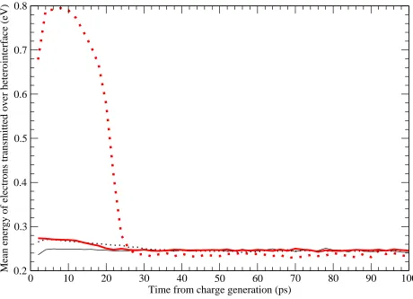
Where figure 5 only shows the latter process, figure 6 clearly demonstrates in which doping
combination the former process is dominant. This figure also highlights how the highly
0.0 0.1 0.2 0.3 0.4 0.5 0.6 0.7 0.8 0.9 1.0
Distance from heterointerface (µm)
0 20 40 60 80 100 120 140
[image:12.612.75.540.318.659.2]Energy dissipated from sampled ensemble (a.u.)
FIG. 5. Spatial histogram of net energy transferred from electrons to lattice via electron-phonon
scattering, for the doping type (p-type: dotted, n-type: solid) and density combinations (thick/red:
doped p-type case has another potential side-effect: the mean energy of electrons entering
the Si layer is significantly higher, improving the chances of rapid impact-ionization.
0 10 20 30 40 50 60 70 80 90 100
Time from charge generation (ps) 0.2
0.3 0.4 0.5 0.6 0.7 0.8
[image:13.612.73.533.115.448.2]Mean energy of electrons transmitted over heterointerface (eV)
FIG. 6. Mean energy of electrons traversing heterointerface as a function of time, for the
dop-ing type (p-type: dotted, n-type: solid) and density combinations (thick/red: higher dopdop-ing,
thin/black: lower doping) of figures 3, 4 and 5. Energy is relative to lowest conduction band
minima.
B. Influence of tunnelling
As stated in section II, two tunnelling mechanisms were considered in addition to the
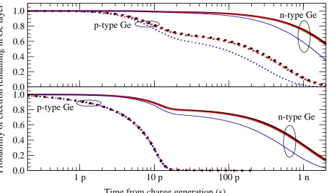
classical transmission over theL state barrier. The effect of including the direct tunnelling on the transmission timescales of figure 4 are shown in figure 7. The degree of tunnelling
is parameterised by the electric field in the Si charge layer, the absolute values used in
the simulation being a sum of the electric field at the heterointerface according to the
and the Si charge layer doping density (in the triangular barrier approximation). The
different thicknesses (colours) of lines in figure 7 therefore allow analysis of the significance
of tunnelling for two different Si charge layer doping densities. It is apparent that, for the
lower density of Si charge layer doping (≈1017cm−3) tunnelling has a negligible impact on the transport timescales. For the higher density of Si charge layer doping (≈1018cm−3), tunnelling has the greatest impact for the cases where the electronic transport is rather slow
such as the long time-scale behaviour mentioned in section III A. Even in this case, while
the improvement is much more apparent, the effect is not as significant as that which may
be achieved by increasing the Ge absorption layer doping density. Higher Si charge layer
densities have not been considered, since other device design and processing constraints
indicate this is not feasible.
Phonon-assisted tunnelling was found to have even less effect than direct tunnelling,
producing an enhancement in Ge to Si transfer probabilities only of the order of a few percent.
Given that both tunnelling processes appear to only weakly improve slow-performing cases
and have little impact on efficient cases, tunnelling was not included in the calculations
described below.
C. Biasing beyond the just-active point
Biasing above the operating point at which the whole Ge layer becomes active leads to
a rigid shift in the electric field profile. Given this, applying a higher bias to the cases from
figure 4 with low doping will allow the electric field near to the heterointerface to reach
the level of that in the p-type high doping case; simulation results which test this idea are
shown in figure 8. The top two thin lines are reproductions of the data from figure 4 for
low background doping, for n-type (solid) and p-type (dotted) dopants; the lower thin lines
are also in pairs and are the result of increasing the electric field profile of these first two
lines in steps of 106V m−1 each time, as the lines drop towards the bottom left of the figure. While the matching is by no means perfect, and this figure uses a logarithmic scale for
the probability, there is a rather good overlap between the p-type (dotted) line from any
given set and the n-type (solid) result from the pair at the next higher electric field (closer
to the bottom-left). From considering the electric field profiles (similar to figure 3) it is
0.0
0.2
0.4
0.6
0.8
1.0
1 p
10 p
100 p
1 n
0.0
0.2
0.4
0.6
0.8
1.0
Time from charge generation (s)
Probability of electron remaining in Ge layer
n-type Ge
p-type Ge
[image:15.612.79.539.69.339.2]n-type Ge
p-type Ge
FIG. 7. Probability of a photo-generated electron remaining in a just-active Ge absorption layer
as a function of time, and tunnelling barrier electric field. The upper plot is for a peak electric
field (doping density) in the Ge layer of 106V m−1 (≈1015cm−3); the lower plot is for 107V m−1 (≈1016cm−3). The thickest (black), thick (red) and thin (blue) lines represent additional
elec-tric field variation (as per equation 1) in the Si charge layer of zero (no tunnelling), 107V m−1 (≈1017cm−3) and 108V m−1 (≈1018cm−3) over the 100 nm Si charge layer.
heterointerface is identical. Furthermore, in the bottom-middle of figure 8 it is also clear
that two (one solid, one dotted) of these thin lines overlay the thick dotted line, which is
a repeat of the high-density p-type result from figure 4. These three results were obtained
from simulations with electric field profiles with differing electric field gradients, but all had
identical values at the heterointerface. All of this supports the earlier suggestion that the
electric field near to the heterointerface is the dominant factor for achieving rapid (<20 ps) transport timescales.
One additional point evident from figure 8 is that while the just-active high p-type doping
case from earlier (figure 4) has 99 % transmission within 20 ps, it also has a long-time tail
for the remaining 1 %. This emphasises the dominance of the electric field at the interface in
1 p 10 p 100 p 1 n Time from charge generation (s)
0.001 0.010 0.100 1.000
[image:16.612.77.539.73.401.2]Probability of electron remaining in Ge layer
FIG. 8. Probability of a photo-generated electron remaining in a just-active Ge absorption layer
as a function of time, for various electric field profiles. The thickest dotted (red) line is for p-type
doping at a density of 1016cm−3 (as lowest line in figure 4). The top two thin (black) lines are for n-type (solid) and p-type (dotted) doping at a density of 1015cm−3 (thin/black lines in figure 4).
Pairs of solid and dotted lines (each pair a different colour) below the top two represent increasing
the entire electric field profile by 106V m−1 for each pair (colour); pairs closer to the thick dotted
line correspond to higher electric fields, equivalent to increasing the reverse bias.
through a set of curves indexed by this parameter.
D. Preferred Ge absorber doping
The results from section III C offer a perspective beyond that of III A, suggesting that as
long as the electric field at the interface can be adequately adjusted, through applying a bias
will suffice. However, this condition only concerns efficient transmission of electrons over the
heterointerface; in practice there are various other constraints which must be met in order
to achieve SPAD operation.
As indicated in section I, one reason for the SACM (or SAM) design of SPADs is to be
able to minimise the electric field in the narrow band-gap material of the absorber layer, so
limiting carrier generation and dark current from band-to-band (Zener) tunnelling. While
similar transmission characteristics may be obtained for a broad range of uniform dopant
type and density combinations so long as the electric field is identical at the heterointerface,
the dopant characteristics affect the gradient of the electric field throughout the Ge absorber
layer. The band-to-band tunnelling rate increases exponentially with electric field17, hence
p-type background doping in the Ge absorber is preferable to n-type since this results in
lower electric fields in the bulk of the layer compared to that at the interface.
According to figures 4 and 8, doping that results in an interfacial electric field of
4×10⁶V m−1 to 107V m−1 should exhibit transmission of ≈ 90 % to 99 %, respectively, of electrons over the interface within 20 ps of being photo-generated. For a 1µm Ge
ab-sorption layer to be just-active and meet these criteria would require p-type doping of
4×1015cm−3 to 1016cm−3 respectively. Biased appropriately, this simultaneously achieves rapid transport of photogenerated electrons while minimising electric-field-enhanced dark
events. A lower background doping density (4×1015cm−3) results in a lower internal electric field (hence potentially lower band-to-band tunnelling), but also a lower transport efficiency
(90 %). Through higher reverse biasing, the interfacial electric field may then be raised
so as to achieve 99 % transmission within 20 ps, yet at the cost of increased band-to-band
tunnelling. Conversely a higher doping density (1016cm−3) results in high transmission in tandem with a minimised internal electric field. Whilst this implies that a higher
dop-ing density is preferable, a high background doping density is often associated with poor
crystalline quality and hence increased dark events.
E. Jitter calculations
Jitter in a SPAD represents the variability in the delay from photon absorption to the
point where a current may be measured, which may be experimentally determined by taking
number of detection events1. Our Monte Carlo simulations can be used to estimate the
contribution to jitter due to variations in transit time from the point of photogeneration in
the Ge to entry into the Si layer.
The histograms required can be easily calculated by taking the derivative of the
trans-mission time data as presented in figures 4 and 8, leading to results such as in figure 9. An
0 10 p 20 p 30 p 40 p 50 p 60 p
Time from charge generation (s)
10-7
10-6
10-5
10-4
10-3
Number of heterointerface transmission events per unit time (a.u.)
0.5 µm
1.0 µm
[image:18.612.73.540.213.547.2]2.0 µm
FIG. 9. Histograms of the number of events requiring a given time from charge generation to
interfacial transmission, allowing comparison of the contribution to jitter for transport in three
different Ge absorber layer heights. Results are for just-active Ge layer conditions, with an electric
field of 107V m−1 at the heterointerface and zero at the top of the layer, corresponding to uniform p-type doping of ≈1016cm−3 for the 1µm case, and an appropriately scaled amount for the others
according to equation 1. These conditions were selected for comparision since the jitter cannot
be determined when the interfacial transport is too low, and does not vary significantly when the
initial rise and later sharp drop (to levels below 10−5) is identifiable for all heights of Ge layer, however each curve typically has two peaks: one at very short times (<2 ps) and a later broader one. The former is associated with velocity overshoot of a sub-ensemble of
electrons which are generated close to the interface. Selecting either peak for a FWHM
measurement does not result in consistent meaningful jitter values.
Jitter values have previously been given for peak heights other than half-maximum31;
given this precedent we determine limiting values of jitter for a range of histograms similar
to those in figure 9. The minimum jitter is calculated by taking the time at which a horizontal
line drawn through the minimum between the two peaks intersects the falling edge, while
the maximum width is taken as that at which the histogram signal enters the noise. The
resulting values for a range of Ge layer heights are shown in figure 10, under the same
conditions as in figure 9; understanding the dependence upon absorber height is relevant
since this is a future route to improving overall optical absorption and detection efficiency,
particularly at longer wavelengths. The shaded region is obtained by approximate linear
fits of the limiting values and reproduces the simulation results remarkably well. The upper
bound passes very close to the origin, indicating the good quality of the data and linear fit.
The fit lower bound intercepts the horizontal axis at 0.25µm, for which simulations confirm that the two peaks merge, supporting the prediction from the fit that this bound approaches
zero. With a single peak the standard FWHM jitter may be determined and was found to
be 1.57 ps.
The relative significance of the jitter components determined above will vary according
to other jitter contributions in the system. These could include those due to the
multipli-cation process itself32,33, including expansion of the current filament34, or those external to
the active device. For thick Ge absorption layers the contribution to jitter from the
pro-cesses modelled here could become significant in otherwise low-jitter designs1 or operating
conditions34.
IV. CONCLUSIONS
Monte Carlo electronic transport simulations have been employed to analyse the impact
of Ge absorber doping on performance characteristics of Ge/Si SPADs. Doping directly
0.0 0.2 0.4 0.6 0.8 1.0 1.2 1.4 1.6 1.8 2.0 Ge layer height (µm)
0 5 10 15 20 25 30 35 40
[image:20.612.73.539.68.408.2]Jitter contribution from Ge layer (ps)
FIG. 10. Estimated range of jitter for various Ge absorber layer heights. The shaded band
rep-resents the range of jitter values between these limits, using a linear fit for the upper and lower
bound.
which is found to be the dominant factor in minimising the time that photo-generated
electrons spend in the Ge. Nevertheless, p-type doping is preferable to n-type, since it allows
the device to be biased such that the electric field is high enough at the Ge/Si interface
to achieve rapid electron transfer into the Si layer, yet which is low enough elsewhere to
minimise dark events from tunnelling. The ideal density of p-type dopants for rapid charge
transport varies according to the height of the Ge absorber layer; for a 1µm thick layer
as primarily analysed here, a density of ≈4×1015cm−3 to 1×1016cm−3 should achieve a transport efficiency of 90 % to 99 % respectively within 20 ps, when the layer is just-active.
Higher efficiencies will occur as the bias is raised, at the cost of increased dark events from
tunnelling and the potential for breakdown to occur in the Ge rather than the Si layer.
layer. However, if the background doping is n-type, it may be desirable to compensate this
with identical p-type doping in order to achieve the optimum electric field profile described
above.
The contribution to jitter from the Ge/Si heterointerface is difficult to ascertain, but
does not appear to vary significantly with bias or doping for conditions under which devices
are expected to function. The jitter contribution varies linearly with the Ge absorber layer
height and the estimated minimum jitter approaches 27 ps for a 2µm high Ge absorber layer,
which is of the same order of magnitude as the minimum jitter found in some experimental
devices34.
ACKNOWLEDGMENTS
This work has been funded by the UK Engineering and Physical Sciences Research
Coun-cil (EPSRC) programme, “UK Silicon Photonics”. The authors acknowledge useful
discus-sion with Gerald Buller and Ryan Warburton (Heriot-Watt University), David R Leadley
and Maksym Myronov (University of Warwick) and Helen Rafferty (University of Leeds).
REFERENCES
1G. S. Buller and R. J. Collins, Measurement Science and Technology 21, 012002 (2010).
2E. Knill, R. Laflamme, and G. J. Milburn, Nature 409, 46 (2001).
3C. H. Bennett and G. Brassard (Bangalore, India, 1984) pp. 175–179.
4S. Bellis, C. Jackson, and A. K¨onig, Laser+Photonik , 34 (2005).
5J. S. Massa, A. M. Wallace, G. S. Buller, S. J. Fancey, and A. C. Walker, Optics Letters
22, 543 (1997).
6A. Tosi, F. Stellari, A. Pigozzi, G. Marchesi, and F. Zappa, in Reliability Physics
Sympo-sium Proceedings, 2006. 44th Annual., IEEE International (2006) pp. 595 –601.
7S. Cova, M. Ghioni, A. Lacaita, C. Samori, and F. Zappa, Applied Optics35, 1956 (1996).
8B. F. Levine, C. G. Bethea, and J. C. Campbell, Electronics Letters 20, 596 (1984).
9Y. Maruyama and E. Charbon, in Solid-State Sensors, Actuators and Microsystems
Con-ference (TRANSDUCERS), 2011 16th International (2011) pp. 1180 –1183.
11Y. Kang, H.-D. Liu, M. Morse, M. J. Paniccia, M. Zadka, S. Litski, G. Sarid, A. Pauchard,
Y.-H. Kuo, H.-W. Chen, W. S. Zaoui, J. E. Bowers, A. Beling, D. C. McIntosh, X. Zheng,
and J. C. Campbell, Nat Photon 3, 59 (2009).
12P. C. M. Owens, J. G. Rarity, P. R. Tapster, D. Knight, and P. D. Townsend, Applied
Optics 33, 6895 (1994).
13A. Lacaita, P. A. Francese, F. Zappa, and S. Cova, Applied Optics 33, 6902 (1994).
14Z. Zhou, C. Li, H. Lai, S. Chen, and J. Yu, Journal of Crystal Growth 310, 2508 (2008).
15V. Shah, A. Dobbie, M. Myronov, and D. Leadley, Solid-State Electronics62, 189 (2011).
16V. M. Robbins, T. Wang, K. F. Brennan, K. Hess, and G. E. Stillman, Journal of Applied
Physics 58, 4614 (1985).
17D. A. Ramirez, M. M. Hayat, and M. A. Itzler, IEEE Journal of Quantum Electronics
44, 1188 (2008).
18C. Jacoboni and L. Reggiani, Reviews of Modern Physics 55, 645 (1983).
19N. J. Pilgrim, W. Batty, and R. W. Kelsall, Journal of Computational Electronics 1, 263
(2002).
20T. Sadi, R. Kelsall, and N. Pilgrim, IEEE Transactions on Electron Devices 53, 1768
(2006).
21N. J. Pilgrim, A. Khalid, G. M. Dunn, and D. R. S. Cumming, Semiconductor Science
and Technology 23, 075013 (2008).
22N. J. Pilgrim, A. Khalid, C. Li, G. M. Dunn, and D. R. S. Cumming, physica status solidi
(c) 8, 313 (2011).
23C. Jacoboni, F. Nava, C. Canali, and G. Ottaviani, Physical Review B 24, 1014 (1981).
24G. H. Li, A. R. Go˜ni, K. Syassen, and M. Cardona, Physical Review B 49, 8017 (1994).
25C. G. Van de Walle and R. M. Martin, Physical Review B 34, 5621 (1986).
26J. Liu, D. D. Cannon, K. Wada, Y. Ishikawa, D. T. Danielson, S. Jongthammanurak,
J. Michel, and L. C. Kimerling, Physical Review B 70, 155309 (2004).
27M. Rouvi`ere, M. Halbwax, J.-L. Cercus, E. Cassan, L. Vivien, D. Pascal, M. Heitzmann,
J.-M. Hartmann, and S. Laval, Optical Engineering 44, 075402 (2005).
28T. Gonz´alez and D. Pardo, Solid-State Electronics 39, 555 (1996).
29M. M. Rieger and P. Vogl, Physical Review B 48, 14276 (1993).
30E.-j. Bai and Q.-q. Shu, Chinese Physics Letters 15, 862 (1998).
Mc-Carthy, M. G. Tanner, J. A. O’Connor, C. M. Natarajan, S. Miki, M. Sasaki, Z. Wang,
M. Fujiwara, I. Rech, M. Ghioni, A. Gulinatti, R. H. Hadfield, P. D. Townsend, and G. S.
Buller, New Journal of Physics 13, 075008 (2011).
32S. L. Tan, D. S. Ong, and H. K. Yow, Journal of Applied Physics 102, 044506 (2007).
33D. Dolgos, H. Meier, A. Schenk, and B. Witzigmann, Journal of Applied Physics 110,
084507 (2011).
34M. Assanelli, A. Ingargiola, I. Rech, A. Gulinatti, and M. Ghioni, IEEE Journal of
1.1
1.2
1.3
1.4
1.5
1.6
1.7
1.8
1.9
2.0
2.1
Relative energy (eV)
1.0
1.5
2.0
2.5
3.0
3.5
4.0
4.5
Relative energy (eV)
Γ
L
Δ
Si
G
Si
Ge
Δ
L
L
Δ
0.0
0.1
0.2
0.3
0.4
0.5
0.6
0.7
0.8
Distance from heterointerface (
μ
m)
0
1
2
3
4
5
6
7
8
9
10
Electric-field in just-active state (10
6