Article
Temporal Encoding to Reject Background Signals
in a Low Complexity, Photon Counting
Communication Link
Alexander D. Griffiths1,* , Johannes Herrnsdorf1 , Christopher Lowe2, Malcolm Macdonald2,
Robert Henderson3, Michael J. Strain1 and Martin D. Dawson1
1 Institute of Photonics, University of Strathclyde, Glasgow G1 1RD, UK; [email protected] (J.H.);
[email protected] (M.J.S.); [email protected] (M.D.D.)
2 Department of Mechanical & Aerospace Engineering, University of Strathclyde, Glasgow G1 1XJ, UK;
[email protected] (C.L.); [email protected] (M.M.) 3 CMOS Sensors & Systems Group, University of Edinburgh, Edinburgh EH9 3JL, UK;
* Correspondence: [email protected]
Received: 14 August 2018; Accepted: 6 September 2018; Published: 9 September 2018
Abstract:Communicating information at the few photon level typically requires some complexity in the transmitter or receiver in order to operate in the presence of noise. This in turn incurs expense in the necessary spatial volume and power consumption of the system. In this work, we present a self-synchronised free-space optical communications system based on simple, compact and low power consumption semiconductor devices. A temporal encoding method, implemented using a gallium nitride micro-LED source and a silicon single photon avalanche photo-detector (SPAD), demonstrates data transmission at rates up to 100 kb/s for 8.25 pW received power, corresponding to 27 photons per bit. Furthermore, the signals can be decoded in the presence of both constant and modulated background noise at levels significantly exceeding the signal power. The system’s low power consumption and modest electronics requirements are demonstrated by employing it as a communications channel between two nano-satellite simulator systems.
Keywords:LED; GaN; single-photon avalanche diode; optical communications; CubeSats
1. Introduction
Conventional optical wireless communications (OWC) involves the modulation of the optical emission from a light source, such as a light-emitting diode (LED) or laser, and detection of the output light with a photoreceiver [1]. When transmitting over long distances, or through high loss media, received power will become greatly reduced, and eventually be lost in noise from background light or within the receiver electronics themselves. Single photon detection and counting methods are used to achieve high receiver sensitivity with intensity modulated optical signals [2–6]. With the use of forward error correction (FEC) codes and high order pulse position modulation (PPM) [7], photon counting systems can operate with extremely low numbers of photons per bit [8]. In combination with arrayed receivers, the high sensitivity of single photon counting techniques has potential for deep-space communication links, operating at megabit rates [9,10].
The link performance of a single photon counting link can suffer significantly under the presence of noise counts [11], which can occur due to background light in the channel, or dark counts occurring within the detector. These additional counts cause erroneous detection of bits, necessitating the use of powerful FEC codes [2,12]. Photon counting links using coincident photon pairs can overcome noise limitations [13–16], and can be used for quantum key distribution [17–19]. However, such
systems typically require high efficiency photon pair sources, putting large form factor requirements on the internal and transceiver optics. In fact, many single photon communication links make use of complex, large, and/or costly equipment, such as cryogenic receivers [3,10], CW lasers with external modulators [2,6] and arbitrary waveform generators [4]. This makes such systems difficult to deploy in application areas where size, weight and power budgets may be limited.
Here, we demonstrate a novel optical transmission scheme, suitable for OWC with single photon detection, requiring a single, low photon flux channel. Compared with existing methods, this scheme is implemented with simple and widely available semiconductor components and electronics. A gallium nitride (GaN) micro-LED transmitter, silicon single-photon avalanche diode (SPAD) receiver and field-programmable gate array (FPGA) electronics provide a compact system and with low power consumption. The transmission method operates under the presence of both constant and modulated background noise, which is enabled by the encoding of data in the timing statistics of the received photons. The following sections discuss the details of the transmission scheme, its current implementation, data transmission results and a demonstration of the system’s suitability for
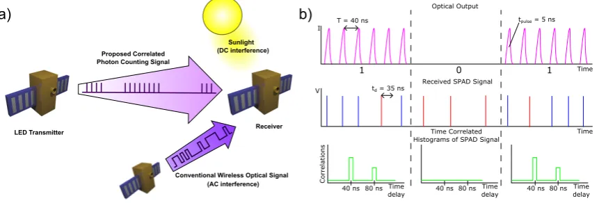
inter-satellite communications, such as shown in Figure1a.
0
1 1
T = 40 ns
Optical Output
Received SPAD Signal
Time Correlated Histograms of SPAD Signal
40 ns 80 ns 40 ns 80 ns 40 ns 80 ns I
Time V
Corr
elat
ions
a)
b)
Sunlight
Conventional Wireless Optical Signal Proposed Correlated
Photon Counting Signal
LED Transmitter Receiver
td = 35 ns
Time
Time
delay delayTime Timedelay tpulse = 5 ns
(DC interference)
[image:2.595.85.516.312.458.2](AC interference)
Figure 1. (a) Application scenario for inter-satellite communications: the proposed signal encodes data in trains of time-correlated optical pulses and is compatible with low power consumption LED emitters. It is resilient against constant background such as sunlight and also insensitive to most AC background such as conventional wireless optical signals. (b) Schematic of the transmission scheme used. LED output on transmission of “0” and “1” (top), SPAD response to the LED signal (middle) and the calculated correlation histograms for each data interval (bottom).
2. Results
2.1. Time Correlation Encoding Scheme
The transmission scheme presented here, inspired by time-correlated single photon counting (TCSPC) techniques often used for fluorescence lifetime imaging [20], involves the use of a single SPAD to receive time correlated signals at a single photon level. Analysis of the SPAD response to incoming
light over an interval[−t1,t1]shows that the correlation count density functiong(τ)dt0of recording
two subsequent SPAD counts with temporal separation in the interval[τ,τ+dt0]is given by:
g(τ) =
Z t1
−t1
dt f(t)f(t+τ). (1)
Here,f(t)is the temporal probability distribution of received SPAD pulses, which is determined
by the optical signal from the transmitter. Full analysis is given in the Supplementary Materials of
Reference [21]. If a suitable optical source transmits pulses with a time separation ofT,g(τ)will
Equation (1) is the autocorrelation of f(t), so it is expected that peaks ing(τ)would have a width
of 2tpulse, wheretpulseis the width of the optical pulse. After detection of a photon, the output of a
SPAD has a “dead time” (τd) in which it is insensitive to further photons, typically 10 s of ns in length
[6,12]. It is important thatT>τd, as otherwise the SPAD would not recover from the first pulse in
time to see the second. This restriction can be lifted by using a SPAD array [22,23], however here
we consider the use of only a single SPAD. The presence and/or temporal position of peaks ing(τ)
directly depends on the sequence of optical pulses from the transmitter, and therefore can be used as a means of transmitting data.
In reality, the SPAD output is not a continuous probability distribution, but a series of discrete photon detection events. These events can occur due to the optical pulses from the transmitter, background photons, or dark counts. SPADs typically have dark count rates (DCRs) ranging from 100 s of Hz to several kHz [2,6,7,12], however, the SPAD used in the following experimental sections has an active cooling system, reducing the DCR to 25 Hz. The SPAD output signal will be sampled
over a time period, intoNstime binsti,i=1, . . . ,Ns, chosen to be smaller thanτd, so that bin contains
a number of counts fi ∈[0, 1]. The correlation time will also be discretised intoτj,j=1, . . . ,Nτ. For a
single pair of pulses a correlation either is or is not detected, so the optical signal must be repeated many times to distinguish correlation counts from noise. Instead of a single pulse pair, the pulses are
continuously repeated at a rate specified by the temporal separationRpulse =1/T. With correlation
time bin size chosen as an integer multiple of sampling bin size,τbin =ktbin, we can define start and
stop indices for correlating acrossi asnstart = τ1/tbin andnstop = nstart+kNτ−1. With this, the
discrete form of Equation (1) is:
g(τj) = Ns−nstop
∑
i=1
k−1
∑
l=0
fifi+nstart+(j−1)k+l. (2)
Asfiis a binary value, and the output from the SPAD is a transistor-transistor logic (TTL) signal,
the summation could be implemented with simple logic circuits.
Encoding data ing(τj)has the potential to allow data transfer at exceptionally low light levels,
and in the presence of significant background illumination. To detect correlations, the receiver requires the detection of a single photon from each optical pulse. Such conditions allow average received power to be extremely low, in the range of pW. The trade-off in this transmission scheme is that the data rate is expected to be relatively modest, as the optical signal must be repeated several times in order to
generate a distinguishable signal ing(τj).
There are several potential ways to encode data ing(τj), with parallels to on-off keying (OOK),
PPM or pulse amplitude modulation (PAM). Here, we consider the simplest form of encoding, OOK, where data can be encoded using a single pulse time separation. On transmission of the symbol
“1”, pulses are transmitted continuously with a fixed time separationT=40 ns, corresponding to a
repetition rate of 25 MHz, sog(τj)will show a peak atτ=T. This time separation has been chosen as
the dead time of the SPAD used is 35 ns. On transmission of the symbol “0” no pulses are transmitted,
producing only background counts ing(τj). A schematic of the expected waveforms is shown in
Figure1b. With pulse widthtpulse = 5 ns, deliberately less thanτd, only one signal photon can be
detected from each pulse, indicated by the blue SPAD signals in Figure1b. In reality, the detection
Synchronisation of the system can be easily achieved by using an embedded clock in the transmitted
data, as discussed in Section4.2.
2.2. Experimental Demonstration
The scheme detailed above was realised using a GaN violet emitting (405 nm), micro-LED device as the transmitter and a silicon Single Photon Avalanche Detector (SPAD) as the receiver. The LED chip was bonded to a custom CMOS driver allowing short pulse operation, with durations of 5 ns. The LED wavelength of 405 nm was initially used as the devices showed improved pulsed performance in this configuration over other wavelength counterparts. Data signal modulation was applied as a slower
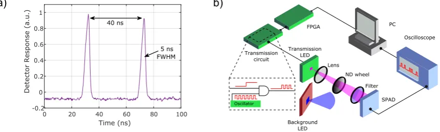
on-off keying of the short pulse train. Figure2a shows a measured pair of pulses from the micro-LED
of 5 ns duration and with a relative delay of 40 ns. A variable neutral density filter was placed between the emitter and detector to control the received power at the SPAD. A schematic of the measurement
setup is shown in Figure2b. Full details of the devices and electronic drivers are given in Section4.1.
0 20 40 60 80 100
Time (ns)
-0.2 0 0.2 0.4 0.6 0.8 1
Detecto
r Response (
a.u.) 40 ns
5 ns FWHM
a)
b)
Oscilloscope
SPAD Filter ND wheel Lens FPGA
Transmission circuit
Background LED
Oscillator
PC
[image:4.595.85.515.287.416.2]Transmission LED
Figure 2.(a) Measured pulse pair from a micro-LED source. (b) Schematic of the experimental setup.
2.3. Signal-to-Noise Ratio
To set an operation threshold for the system, a figure of merit similar to the classical signal-to-noise ratio (SNR) must be defined. In this method, it is the distinguishability of the correlation peak
in the g(τ) function that indicates the robustness of the classical information recovery to noise.
Conventional SNR can be defined asSNR=10 log10 NNsignal
noise, whereNsignalis average signal correlation
counts andNnoiseis average noise correlation counts. However, as the number of pulse repetitions
increases, the correlation counting interval increases, causing bothNsignalandNnoiseto increase at linear
rates. This results in a constant SNR, which does not reflect the observed increase in distinguishability of signal correlations with increasing pulse repetitions.
Instead, it is more useful to consider the statistical distribution of correlation counts for signal and noise. Photon counting experiments were undertaken using the experimental setup described above, with a received power at the detector of 38 pW, corresponding to a detector count rate of
1.07×10⁷Hz, in a dark lab environment with an average background count rate of 619 Hz. Note that
this count rate contains both dark counts and counts from the small amount of ambient light. The delay correlations of detected photons were binned with a resolution of 10 ns, with the transmitted pulse
delay set at 40 ns. Figure3a,b shows average histograms of received photon correlations for 5 and 100
pulse repetitions, respectively. Figure3c shows the histogram for 100 pulse repetitions under high
background conditions, displaying the correlation histogram due to background noise alone, and
signal with noise. The background count rate for this measurement was 107Hz.
In Figure3a–c, the signal is defined as the number of correlations in the 40 ns delay time bin, and
the noise correlation count is taken from the 60 ns delay bin. Correlation counts follow a Poissonian distribution, as they are discrete independent events arising directly from shot noise limited photon
correlation counts at 5 and 100 repetitions of the pulses, respectively, taken from 1500 independent
measurements of each case. Figure3f shows the distributions for background noise, signal alone
(identical to Figure3e) and combined signal and noise.
5 repetitions
20 40 60 Time (10 ns bins) (ns) 0
5 10 15
Mean correlation counts
100 repetitions
20 40 60 Time (10 ns bins) (ns) 0
5 10 15
Mean correlation counts
0 5 10 15 20 25 Correlation counts 0 0.5 1 Probability 5 repetitions
Signal + noise Noise
0 5 10 15 20 25 Correlation counts 0 0.5 1 Probability 100 repetitions
Signal + noise Noise
0 20 40 60 80 100 Pulse repetitions 10-6 10-4 10-2 100 Poissonian overlap
0.1 0.2 0.3 0.4 Photons detected per pulse 10-6
10-4 10-2 100
Poissonian overlap
0 10 20 30
Correlation counts 0 0.05 0.1 0.15 0.2 Probability
100 repetitions with noise
Signal + noise Noise Signal
100 repetitions with noise
20 40 60 Time lag (10 ns bins) (ns) 0
5 10 15 20
Mean correlation counts
Signal + noise Noise
0 1 2 3 4 5
Mean noise correlations 10-8
10-6 10-4 10-2
Possonian overlap
a) b) c)
d) e)
g)
f)
[image:5.595.98.499.163.469.2]h) i)
Figure 3.Measured correlation histograms for: (a) 5 pulse repetitions; (b) 100 pulse repetitions; and (c) 100 pulse repetitions with background noise. Poissonian distributions for the signal and noise correlation counts for: (d) 5 pulse repetitions; (e) 100 pulse repetitions; and (f) 100 pulse repetitions with background noise. (g–i) Poissonian overlap according to Equation (3) as a function of: (g) number of pulse repetitions; (h) average number of photons detected per pulse; and (i) average number of background noise correlations.
At five repetitions, the probability distributions for signal and noise are strongly overlapped. Thus, a correlation count peak due to signal transmission is difficult to distinguish from a correlation count peak due to random background and dark counts. At 100 repetitions, the overlap of signal and noise distributions is significantly reduced, making distinction much easier. A histogram threshold equates to a point along the x-axis of the distribution plots. Evidently, a threshold of 2 would result in many erroneous detections at five repetitions, whereas, at 100 repetitions, the majority of signal correlation peaks would be correctly identified, and noise correlation peaks rejected. Under high background noise conditions, the number of correlations from noise is increased, so the threshold must increase to distinguish between the correlations due to noise from those due to the signal, as both will be present on transmission of “1”.
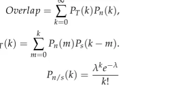
Distinguishability is therefore described by Equation (3), the overlap of the Poisson distributions
for: (i) the total signal and noise contributions,PT(k); and (ii) the noise alone,Pn(k).PT(k)is related to
are the the probabilities ofkcorrelation counts occurring due to noise or signal with meanλ, given by
Equation (5).
Overlap=
∞
∑
k=0
PT(k)Pn(k), (3)
PT(k) = k
∑
m=0
Pn(m)Ps(k−m). (4)
Pn/s(k) = λke−λ
k! (5)
Figure3g–i shows the calculated overlap for changing pulse repetitions, photon detection rate and
noise correlations, respectively. The overlap reduces exponentially with pulse repetitions, faster than exponential with photon detection rates, and increases sub-exponentially with background correlations.
This is understood by noting thatλin Equation (5) followsλ= p2phNrep, wherepphis the probability
of detecting a photon from a single pulse, andNrepis the number of pulse repetitions.
Therefore, the distinguishability of binary 0 and 1 is governed by the Poissonian overlap, Equation (3), and depends on the number of sampled pulse repetitions, the received signal power, and the background intensity, with the first two parameters dominating.
2.4. Data Rates
The achievable data rate of this system is determined by the number of pulse repetitions required to distinguish the signal, and hence the received power and the time separation between pulses.
The SPAD response imposes a lower limit on this separation, due to the dead timeτdand pulse width,
τpulse, giving an achievable data rate of:
Rdata=
1
Nrep(tpulse+τd)
. (6)
whereNrepis the number of pulse repetitions required to see a distinguishable peak in the correlation
histogram. Use of a SPAD array could lift the restrictions imposed by dead time through pulse combining techniques [23]. To demonstrate the system performance as a function of received power
and data rate, bit error ratio (BER) measurements were taken. A target BER of 1×10⁻³was used,
as FEC codes can be used to reduce this to effectively error free levels at a small overhead on data
throughput [24]. A pseudo-random bit sequence (PRBS) of 104bits was transmitted, limited by the data
processing capabilities of the oscilloscope and PC components in the measurement setup. The ND filter
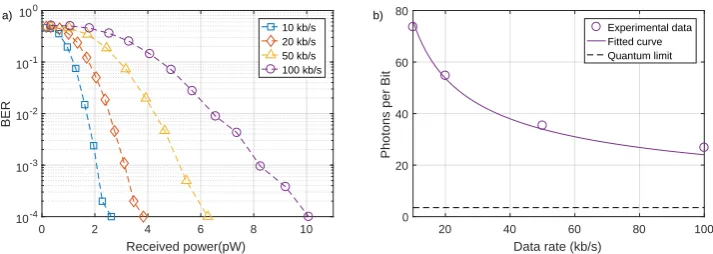
wheel allowed control of received power, or equivalently, photon detection probability. Figure4a shows
BER curves for varying data transmission rates, taken with minimal background light. At 8.25 pW of average power, corresponding to an average of 0.34 incident photons per pulse, a data rate of 100 kb/s
was possible with a BER of less than 10−3. Received optical power can be reduced at the expense of
data rate. A data rate of 10 kb/s can be achieved at the same BER with 2 pW, corresponding to 0.08
photons per pulse. The power measurements quoted here and used in Figures4and5are the incident
optical power on the active area of the SPAD, calculated through numerical methods from the average detector count rate. Detector count rate is the parameter which governs BER performance, however the incident optical power will be influenced by the performance of the SPAD. Most importantly, the photon detection probability (PDP) at 405 nm is 18%, so the incident photon flux is significantly higher than the detector count rate. More efficient photon detection would improve BER performance in terms of required power.
The system performance can also be described in terms of the number of received photons per
bit. Figure4b shows detected photons per bit for each data rate, at the level required for a BER of less
than 10−3. The fitted curve is calculated from the relationship between correlation counts, received
[image:6.595.241.439.134.221.2]and is inversely proportional to the data rateRdata. To reach a given target BER, a certain constant
number of signal correlation counts must be reached, meaning(ph/s)2∝Rdata. As photons per bit is
the required photons per second divided by data rate, the data follows ay=x−12 relationship. The 100
kb/s link is transmitting each bit with an average of 27 detected photons. This is relatively close to the
standard quantum limit (SQL), set by Poissonian photon statistics [25]. For a BER of 10−3, a minimum
of seven photons is required to detect a “1”. Therefore, an average of 3.5 photons per bit is required, assuming the probability of transmitting “0” or “1” is equal. The implemented scheme will be unable to reach the SQL, due to the correlation approach. Two photons are required for a single correlation detection, which itself has a Poissonian distribution that must be distinguished from noise.
0 2 4 6 8 10
Received power(pW) 10-4
10-3 10-2 10-1 100
BER
10 kb/s 20 kb/s 50 kb/s 100 kb/s
20 40 60 80 100
Data rate (kb/s) 0
20 40 60 80
Photons per Bit
Experimental data Fitted curve Quantum limit
[image:7.595.113.470.227.354.2]a) b)
Figure 4.(a) BER as a function of received signal power for varying data rates. (b) Received photons per bit required to achieve a BER of less than 10−3for varying data rates, fitted with ax−12 relationship. The standard quantum limit for OOK at this BER is also shown.
After correcting for detector efficiency, 27 detected photons equate to 7.37×10⁻¹⁷J incident on
the detector per bit. This exceptionally low energy demonstrates the suitability of the transmission scheme in low power or high loss systems. As mentioned above, more efficient photon detection would allow further reductions in energy received per bit. Additionally, efficiency improvements will be possible through use of PPM style transmission, to transmit multiple bits per correlation peak.
2.5. Robustness to Noise
A major advantage of this transmission scheme is that it is expected to be robust against background counts, as ambient light is generally uncorrelated on the time scale of 10 s of ns. To verify this, BER measurements were taken for increasing levels of background light using a secondary 450 nm
light source, as shown in Figure2b. As background counts increase, the probability of detecting
noise correlations increases. The threshold applied to the correlation histogram must be increased to avoid erroneous detection of bits, requiring higher received average power to maintain the same BER performance.
The results in Figure5a show the incident optical power required to maintain a BER of 1×10⁻³
for 10 and 50 kb/s with increasing levels of background optical power. The signal power requirements do increase, however, they are still very low. At high background levels, the required signal power is significantly lower than the power received from background illumination, with equal levels indicated by the solid line. Here, the interplay between number of pulse repetitions, photons detected per pulse
and background counts becomes important. As discussed in Section2.3, higher levels of background
The system was also measured under modulated background illumination. Since the number of detected correlation counts depends on the square of received power, a high modulation rate background should interfere in the same manner as a DC signal at the root-mean-squared (RMS) of its count rate. For this reason, background signals were set to maintain similar RMS photon count rates for comparison to DC measurements. The RMS background optical power was approximately 15 pW for
all measurements. The power required to maintain a BER of 10−3is shown in Figure5b, and displays
two distinct groups of results. The high background modulation rates of 1 and 10 MHz show similar required signal power to constant background conditions, while when the background modulation rate is close to the correlation link data rate, the BER performance is degraded, requiring approximately 40% more received power. This reduction in performance occurs as the background signal is now generating different levels of noise correlations from one bit period to the next, making it more difficult to choose a correlation threshold. At higher background modulation rates the background signal completes many cycles within a single bit period of the correlation link, and the dead time of the SPAD restricts the number of photons that can be detected per background cycle, causing the signal to interfere in the same manner as constant background. Nevertheless, all conditions still reach a BER of
less than 10−3for less than 14 pW of received signal power.
0 10 20 30 40
Background optical power (pW) 0
5 10 15
Signal power for BER 10
-3
10 kb/s 50kb/s
0 5 103
9 10 11 12 13 14
Signal power for BER 10
-3
104 105 106 107 Background modulation frequency (Hz)
[image:8.595.114.469.322.447.2]a) b)
Figure 5.(a) Required signal power to attain a BER of 10−3under constant background power for 50 and 10 kb/s. Equal signal and background power is indicated by the solid line. (b) Required signal power to attain a BER of 10−3under modulated background conditions. Required power increases by approximately 40% when background modulation rates are comparable to the signal data rate.
Under all background conditions, the signal is transmitted with a lower photon count rate than the background signal, demonstrating low power performance even with high power modulated background interference.
2.6. Satellite Systems Demonstration
The communications system presented here is applicable in many scenarios, but is particularly attractive for inter-satellite links. The semiconductor devices are extremely compact, have low power consumption and are readily integrated with control electronics. LED based visible light communications shows potential for use with cube satellites [26,27]. The robustness of the signal to background noise and operation at picowatt levels of received optical power means the scheme could be implemented without the high accuracy pointing requirements, telescope optics and filters of current satellite systems.
To highlight this capability, the system was tested in the nano-satellite hardware and software
test-bed, NANOBED, shown in Figure6a, which can simulate the available power systems on a cube
satellite. To demonstrate that the full communication link was able to be powered by the NANOBED, a real time decoder, incorporating embedded clock signal recovery, was implemented on a FPGA platform to replace the oscilloscope and PC components in the characterisation setup. Details of this
The LED transmission system was integrated with one NANOBED system, while the SPAD receiver system was integrated with a second. In this work, the solar panel emulating power sources are used to supply the transmitter and receiver devices via the electrical power supply (EPS) and battery units, simulating an in-orbit scenario. The transmitter side of the real time link requires a single FPGA board, from which the CMOS micro-LED array is powered and controlled. On the receiver side, the commercial SPAD module requires a 6 V DC supply, and a second FPGA is used to process the
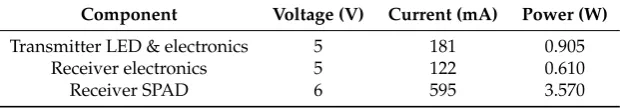
received signals. A summary of typical power consumption is shown in Table1. The SPAD consumes
the most power in the system, however the commercial module has not been designed with power conservation in mind, and employs significant levels of active cooling. A custom SPAD receiver may show power requirements of 10–100 mW [6,22]. While the lack of active cooling would result in
higher levels of dark counts, the resilience to constant background signals demonstrated in Section2.5
indicates this would not be problematic. Additionally, bespoke electronics in place of FPGA boards may also permit lower power consumption, therefore this demonstration should be thought of as an upper limit on power requirements.
SPAD Filter ND wheel Lens
FPGA PC
Transmission LED
FPGA PC
LED transmitter
board NANOBED test bed 3U CubeSatchassis
NANOBED NANOBED
Power Data only
[image:9.595.84.508.295.444.2]10 cm
Figure 6. (a) Photograph of the micro-LED transmitter board (left), NANOBED “Flatsat” test bed (middle) and a standard 3U CubeSat chassis (right). (b) Schematic of the experimental setup for real time data transmission under simulated satellite power.
Table 1.Typical power requirements of the communication system.
Component Voltage (V) Current (mA) Power (W)
Transmitter LED & electronics 5 181 0.905
Receiver electronics 5 122 0.610
Receiver SPAD 6 595 3.570
For the laboratory demonstration, the transmitter and receiver were placed 4 m apart with the micro-LED pixel projecting the light across a 4 cm wide square with received power controlled using a neutral density filter. A micro-LED emitter at 450 nm was used to improve the PDP to 25%. As shown
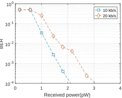
in Figure7, the live link requires 2.5 pW of received power to maintain a BER of 10−3at 20 kb/s.
On a 20 µm diameter SPAD, 3 pW corresponds to an intensity of 9.5 mW/m2. To provide this over the
[image:9.595.143.455.540.594.2]0 1 2 3 4 Received power(pW)
10-4 10-3 10-2 10-1 100
BER
[image:10.595.191.390.94.254.2]10 kb/s 20 kb/s
Figure 7.BER performance of the real-time communication link under simulated satellite power.
3. Discussion
We have demonstrated a transmission scheme suitable for single photon level optical wireless
communications. By transmitting temporally correlated signals, data communications can be
performed at extremely low light levels, with received power on the order of pico-Watts. Signals can be transmitted using an LED, and received with a single SPAD. A 100 kb/s link has been achieved
with a BER of less than 10−3at a received power of 8.25 pW. The scheme is robust to background
light, with only a minor increase in required power for very high background conditions. Modulated background signals appear to have little additional influence over that of continuous background, suggesting the scheme could be used in parallel with other optical communications with minimal interference. Furthermore, multiple transmission systems using this scheme could operate without interfering with each other, simply by using different pulse time separations. The modest data rates presented in this work are dominated by two key factors, firstly the requirement of this protocol for correlating many repetitions of a pulse pattern, and, secondly, the dead time of the SPAD detector itself.
A real time transmission setup has been demonstrated, showing a method for clock synchronisation and determination of a threshold level. The current, unoptimised implementation allows a data rate up to 20 kb/s, with only a minor reduction in performance when compared to offline processed transmission. The real time transmission link has been demonstrated in a simulated
satellite environment, providing data transmission at a received optical intensity of 9.5 mW/m2under
simulated nanosatellite power systems. Additionally, GaN LEDs at low current densities show higher wall-plug efficiencies than laser diode counterparts [28], further enhancing the power consumption characteristics of the system. In future satellite-focussed experiments, an optimum transmission wavelength will be chosen, based on LED performance, detector response and solar-blind wavelengths.
Data rate and photons per bit efficiency can both be improved through relatively straightforward modifications to the system. By using a SPAD array as a receiver rather than a single device, the dead time limitation can be overcome and therefore higher data rates achieved. In addition, by implementing a form of pulse position modulation, with powerful FEC codes, the photons per bit transmission efficiency can be improved. Finally, data rates may be enhanced by using a form of pulse amplitude modulation, however the received power requirement would also increase.
4. Materials and Methods
4.1. Optical Transmitter and Receiver Realisation
The transmitter used for the results presented here is a complementary metal oxide semiconductor (CMOS) integrated gallium nitride micro-LED pixel. Details and fabrication of comparable devices can
be found in [29]. The micro-LED pixel is a square 100×100 µm in size, and part of a 16×16 array
with a 405 nm emission wavelength. The array was fabricated in flip chip format, and bump-bonded onto CMOS control electronics which allow the LEDs to be modulated in a pulsed mode, triggered
by the falling edge of an input logic signal. The shortest stable optical pulsestpulse that could be
generated with this device and control system were 5 ns. To produce pulses for the OOK transmission, a data signal was produced at the desired data rate by a field programmable gate array (FPGA) (Xilinx Spartan-3, XEM3010, Opal Kelly, Portland, OR, USA). The FPGA clocks were derived from a 48 MHz signal from a USB microcontroller, with parts of the system running at 100 MHz. The data sequence was sent to a simple transmission circuit. Here, the data signal was combined with an oscillator producing a signal of square waves with a period of 40 ns, through an AND gate, as shown
in Figure2b.
The SPAD receiver is a commercial module (SPCM20A, Thorlabs, Newton, NJ, USA), with a detector active area diameter of 20 µm. The dead time of the detector is 35 ns, and the typical dark count rate is 25 Hz. At 405 nm and 450 nm, the PDP is 18% and 25%, respectively. The module outputs 3 V logic signals indicating photon counts. This signal was sent to an oscilloscope, and collected by the
PC for offline processing ofg(τj). In a practical system, this processing could be performed by digital
logic circuits
The LED output was collected with a lens (C220TME-A, Thorlabs, Newton, NJ, USA) and transmitted through a graded neutral density (ND) wheel (NDC-50C-4M-A, Thorlabs, Newton, NJ, USA). A 450 nm shortpass filter was used in front of the SPAD to reject additional background light. This filter was removed for the experiments assessing performance under high background conditions. The pixel was imaged onto the SPAD active area. As the pixel image is approximately a 7 mm square, only a small portion of the light was imaged on to the SPAD circular active area of diameter 20 µm. In a practical system, receiver optics could be used to collect more light on to the active area of the SPAD, reducing the loss through the channel. Received optical power was calculated numerically from the average number of photon counts detected. This method accounts for detector dead time, and photon detection probability at the operational wavelength. Details of the calculation can be found in the Supplementary Materials of Reference [21].
To assess the effects of DC background illumination, a commercial 450 nm LED (LD CQ7P, OSRAM, Munich, Germany) was placed within a few centimetres of the transmitter LED, directed
towards the SPAD, as shown in the setup schematic in Figure2b. By increasing the driving current for
the commercial LED, the background counts could be controlled. The modulated background optical signal was generated using a commercial 450 nm LED (LERTDUW S2W, OSRAM, Munich, Germany) modulated with a transistor. This commercial LED had a modulation bandwidth of 15.9 MHz, and was placed within a few centimetres of the transmitting LED. Modulating this LED with a PRBS effectively simulates operation of the correlation link in an environment with conventional optical wireless communication links.
4.2. Real Time Link
To demonstrate a practical system, an FPGA based synchronisation system was implemented, involving data transmission in frames consisting of a 6 bit clock word and 32 data bits. The clock word, “001101”, allows both frame level and symbol level synchronisation of data streams. Details on choice of clock work and synchronisation methods can be found in the Supplementary Materials of Reference [21]. A block diagram of the experimental setup for real-time transmission is shown in
the 6 bit clock word. In contrast to the offline setup in Figure2b, this FPGA directly supplied the falling edge trigger for the LED board, without the need for extra logic circuitry. The receiver FPGA (Xilinx Spartan-3, XEM3010, Opal Kelly, Portland, OR, USA) was connected to a separate PC, and clock synchronisation removed the need for a trigger from the transmitter. However, due to limitations from the FPGA boards, the achievable data rates with the real-time setup are limited to 20 kb/s. It should also be noted that the data rates quoted here include transmission of the clock word. This 18.75% overhead reduces useful data transfer to 8.42 and 16.84 kb/s for 10 and 20 kb/s links, respectively.
4.3. NANOBED Satellite Simulator Experiments
The LED transmitter and SPAD receiver systems were independently powered by separate NANOBED systems, positioned approximately 4 m apart. A 450 nm micro-LED was used, focussed on the receiver plane using an 8 mm focal length lens (C240TME-A, Thorlabs, Newton, NJ, USA), giving a pixel image size at of approximately 4 cm. To increase received power on the 20 µm diameter SPAD, a 35 mm focal length collection lens (ACL4532U-A, Thorlabs, Newton, NJ, USA) was used.
The satellite simulator test bed is a FlatSat-configured CubeSat system, which includes an electrical power system, batteries, an on-board computer and communication systems. A software design tool offers mission design, simulation and analysis, including a link to the hardware for in-loop simulation and testing. A software defined radio link to NANOBED enables ground software validation and operational testing, over which command and control of the system components can be invoked. The NANOBED EPS provides a 5 V bus suitable for powering the transmitter and receiver FPGA boards directly. For the SPAD supply, the unregulated battery bus was used with a voltage regulator to fix the voltage to 6 V.
Author Contributions:J.H. and R.H. conceived the approach; experimental implementation, verification and
analysis was performed by A.D.G.; experimental work with the NANOBED system was performed by C.L.; FPGA and MATLABTMsoftware was developed by J.H.; and J.H., M.J.S., M.M and M.D.D. contributed to discussion and interpretation of the results. All authors contributed to the final form of the manuscript.
Funding: This research was funded by UK Engineering and Physical Sciences Research Council (EPSRC)
EP/M01326X/1, UK Quantum Technology Hub in Quantum Enhanced Imaging. The NANOBED environment was developed under funding from UK Space Agency in collaboration with Clyde Space Ltd.
Acknowledgments: The underlying experimental data for the work presented here are available online at
doi:10.15129/0dfcac12-dbf6-424f-8bc7-71d13db00155.
Conflicts of Interest:The authors declare no conflict of interest. The founding sponsors had no role in the design of the study; in the collection, analyses, or interpretation of data; in the writing of the manuscript, and in the decision to publish the results.
References
1. Rajbhandari, S.; Mckendry, J.J.D.; Herrnsdorf, J.; Chun, H.; Faulkner, G.; Haas, H.; Watson, I.M.; Brien, D.O.; Dawson, M.D. A review of Gallium Nitride LEDs for multi-gigabit-per-second visible light data communications. Semicond. Sci. Technol.2017,32, 1–44.
2. Robinson, B.S.; Caplan, D.O.; Stevens, M.L.; Barron, R.J.; Dauler, E.A.; Hamilton, S.A. 1.5-photons/bit Photon-Counting Optical Communications Using Geiger-Mode Avalanche Photodiodes. In Proceedings of the LEOS Summer Topical Meetings, San Diego, CA, USA, 25–27 July 2005.
3. Robinson, B.S.; Kerman, A.J.; Dauler, E.A.; Barron, R.J.; Caplan, D.O.; Stevens, M.L.; Carney, J.J.; Hamilton, S.A.; Yang, J.K.W.; Berggren, K.K. 781 Mbit/s photon-counting optical communications using a superconducting nanowire detector. Opt. Lett.2006,31, 444–446, doi:doi:10.1364/OL.31.000444.
4. Chitnis, D.; Zhang, L.; Chun, H.; Rajbhandari, S.; Faulkner, G.; O’Brien, D.; Collins, S. A 200 Mb/s VLC demonstration with a SPAD based receiver. In Proceedings of the 2015 IEEE Summer Topicals Meeting Series, SUM 2015, Nassau, Bahamas, 13–15 July 2015,3, 226–227, doi:10.1109/PHOSST.2015.7248280. 5. Li, Y.; Safari, M.; Henderson, R.; Haas, H. Optical OFDM With Single-Photon Avalanche Diode. IEEE
6. Zimmermann, H.; Steindl, B. Hofbauer, M; Enne R. Integrated fiber optical receiver reducing the gap to the quantum limit. Sci. Rep.2017,7, 1–12, doi:10.1038/s41598-017-02870-2.
7. Alsolami, I.; Chitnis, D.; O’Brien, D.C.; Collins, S. Broadcasting over photon-counting channels via multiresolution PPM: Implementation and experimental results. IEEE Commun. Lett.2012,16, 2072–2074, doi:10.1109/LCOMM.2012.111612.121935.
8. Boroson, D.M. A survey of technology-driven capacity limits for free-space laser communications.Free-Space Laser Commun. VII2007,6709, 670918, doi:10.1117/12.738310.
9. Mendenhall, J.A.; Candell, L.M.; Hopman, P.I.; Zogbi, G.; Boroson, D.M.; Caplan, D.O.; Digenis, C.J.; Hearn, D.R.; Shoup, R.C. Design of an optical photon counting array receiver system for deep-space communications. Proc. IEEE2007,95, 2059–2069, doi:10.1109/JPROC.2007.905098.
10. Boroson, D.M.; Robinson, B.S. The Lunar Laser Communication Demonstration: NASA’s First Step toward Very High Data Rate Support of Science and Exploration Missions. Space Sci. Rev. 2014,185, 115–128, doi:10.1007/s11214-014-0122-y.
11. Liao, S.K.; Yong, H.L.; Liu, C.; Shentu, G.L.; Li, D.D.; Lin, J.; Dai, H.; Zhao, S.Q.; Li, B.; Guan, J.Y.; et al. Long-distance free-space quantum key distribution in daylight towards inter-satellite communication. Nat. Photonics2017,11, 509–514, doi:10.1038/nphoton.2017.116.
12. Zhang, L.; Chitnis, D.; Chun, H.; Rajbhandari, S.; Faulkner, G.; O’Brien, D.C.; Collins, S. A comparison of APD and SPAD based receivers for visible light communications. J. Lightw. Technol.2018,36, 2435–2442, doi:10.1109/JLT.2018.2811180.
13. Lekki, J.; Nguyen, Q.V.; Bizon, T.; Nguyen, B.; Kojima, J.; Hizlan, M. An Extremely Low Power Quantum Optical Communication Link for Miniature Planetary Sensor Stations. J. Aerosp. Comput. Inf. Commun.2008, 5, 396–408, doi:10.2514/1.35411.
14. Hizlan, M.; Lekki, J.D.; Nguyen, B.V. Glenn Research Center quantum communicator receiver design and development. Opt. Eng.2009,48, 1050031, doi:10.1117/1.3241989.
15. Seward, S.; Tapster, P.; Walker, J.; Rarity, J. Daylight demonstration of low-light-level communication system using correlated photon pairs. Opt. Quantum Electron.1991,3, 201–207.
16. Hong, C.K.; Friberg, S.R.; Mandel, L. Optical communication channel based on coincident photon pairs. Appl. Opt.1985,24, 3877–3882, doi:10.1364/AO.24.003877.
17. Hughes, R.J.; Buttler, W.T.; Kwiat, P.G.; Lamoreaux, S.K.; Morgan, G.L.; Nordholt, J.E.; Peterson, C.G. Free-space quantum key distribution in daylight.J. Mod. Opt.2000,47, 549–562, doi:10.1080/095003400148376. 18. Gordon, K.J.; Fernandez, V.; Townsend, P.D.; Buller, G.S. A short wavelength GigaHertz clocked fiber-optic
quantum key distribution system.IEEE J. Quantum Electron.2004,40, 900–908, doi:10.1109/JQE.2004.830182. 19. Takenaka, H.; Carrasco-Casado, A.; Fujiwara, M.; Kitamura, M.; Sasaki, M.; Toyoshima, M. Satellite-to-ground quantum-limited communication using a 50-kg-class microsatellite. Nat. Photonics
2017,11, 502–508, doi:10.1038/nphoton.2017.107.
20. Becker, W.Advanced Time-Correlated Single Photon Counting Applications; Springer: Berlin, Germany, 2015. 21. Griffiths, A.D.; Herrnsdorf, J.; Lowe, C.; Henderson, R.; Strain, M.J.; Dawson, M.D. Poissonian
communications: Free space optical data transfer at the few-photon level. arXiv2018, arXiv:1801.07994. 22. Fisher, E.; Underwood, I.; Henderson, R. A reconfigurable single-photon-counting integrating receiver for
optical communications. IEEE J. Solid-State Circuits2013,48, 1638–1650, doi:10.1109/JSSC.2013.2253222. 23. Gnecchi, S.; Dutton, N.A.; Parmesan, L.; Rae, B.R.; Pellegrini, S.; McLeod, S.J.; Grant, L.A.; Henderson, R.K.
Digital Silicon Photomultipliers With OR/XOR Pulse Combining Techniques.IEEE Trans. Electron Devices
2016,63, 1105–1110, doi:10.1109/TED.2016.2518301.
24. ITU. Recommendation G.975.1: Forward Error Correction for High Bit-Rate DWDM Submarine Systems; ITU: Geneva, Switzerland, 2005.
25. Shieh, W.; Djordjevic, I.OFDM for Optical Communications; Elsevier: Amsterdam, The Netherlands, 2010. 26. Kawamura, Y.; Tanaka, T. Transmission of the LED light from the space to the ground. AIP Adv.2013,3,
doi:10.1063/1.4824853.
28. Piprek, J. Comparative efficiency analysis of GaN-based light-emitting diodes and laser diodes. Appl. Phys. Lett.2016,109, 2–6, doi:10.1063/1.4958619.
29. Zhang, S.; Watson, S.; McKendry, J.J.D.; Massoubre, D.; Cogman, A.; Gu, E.; Henderson, R.K.; Kelly, A.E.; Dawson, M.D. 1.5 Gbit/s multi-channel visible light communications using CMOS-controlled GaN-based LEDs. J. Lightw. Technol.2013,31, 1211–1216, doi:10.1109/JLT.2013.2246138.
c