Thesis by
Rebecca Wernis
In Partial Fulfillment of the Requirements for the Degree of
Bachelor of Science
California Institute of Technology Pasadena, California
2013
Acknowledgements
No one does research in a vacuum − especially not experimental physicists. Since joining the Zmiudzinas research group in June 2011 I’ve had help in every step of the work presented here. I would first like to thank Prof. Jonas Zmuidzinas for offering me a place in his research group for two years, where I could learn firsthand and take part in all the work that goes into detector development. Next I would like to thank Loren Swenson, a postdoc in Jonas’ group who brought me from a state of knowing nothing about microwave electronics and cryogenics to the point where I could set up and program the instruments and take data on my own. Loren was always available when I had questions or needed help and worked closely with me not only in the data taking but the analysis and interpretation as well, drawing on his considerable knowledge and experience in the field.
Abstract
Contents
Acknowledgements iii
Abstract iv
1 Background 1
1.1 Introduction to bolometers . . . 1
1.1.1 Bolometer modeling . . . 2
1.2 Introduction to superconducting microresonators . . . 2
1.2.1 Microresonator electrodynamics . . . 3
1.2.2 Principles of operation . . . 3
1.2.3 Frequency multiplexing . . . 4
1.2.4 Photon absorption . . . 4
1.2.5 Two level systems . . . 5
1.3 The resonator bolometer . . . 6
1.3.1 Fabrication . . . 7
2 Measurement Techniques 9 2.1 Overview . . . 9
2.2 Measurement setup . . . 9
2.3 Fitting for the resonant frequency and quality factor . . . 11
3 Dark Measurement Results 13 3.1 Temperature dependence . . . 13
3.2 Response . . . 15
3.2.1 Thermal conductance calculation . . . 16
3.2.2 Results . . . 16
3.3 Noise . . . 16
3.3.1 Data collection and processing . . . 16
3.3.3 Dark noise results . . . 19
4 Measurements under illumination 21 4.1 Optical response measurement . . . 21
4.2 Time Constant . . . 21
4.3 Noise under illumination . . . 24
4.4 Noise equivalent power . . . 25
5 Conclusion 27 A Expressions for fr(T) and Qi(T)from Mattis-Bardeen theory 28 A.1 Temperature dependence of fr . . . 28
A.2 Temperature dependence of Qi . . . 29
B Resonator ring-down time derivation 30 C HFSS modeling calculations 31 C.1 Description of circuit . . . 31
C.2 Analytic solution to simplest case . . . 31
List of Figures
1.1 Schematic of a bolometer . . . 2
1.2 Lumped-element resonator pixels and sample readout . . . 4
1.3 ROACH board . . . 5
1.4 Two level systems . . . 5
1.5 Resonator bolometer pixel and explanation . . . 7
1.6 Prototype resonator bolometer array . . . 8
2.1 Measurement setup . . . 10
2.2 Instrument programming with LabVIEW . . . 10
2.3 Data processing steps . . . 12
3.1 Fractional frequency shift and quality factor vs. temperature . . . 14
3.2 Quality factor vs. fractional frequency shift . . . 14
3.3 Data processing steps . . . 15
3.4 Response under dark conditions . . . 17
3.5 Sample noise data . . . 18
3.6 Power spectral density . . . 18
3.7 Noise under dark conditions . . . 20
4.1 Optical response measurement photo . . . 22
4.2 Optical response . . . 22
4.3 Time constant measurement photo . . . 23
4.4 Time constant measurement . . . 23
4.5 Fractional frequency noise under dark and illuminated conditions at constant temperature 24 4.6 Noise under illumination . . . 25
4.7 Illuminated and dark noise equivalent power . . . 26
Chapter 1
Background
Cryogenic detectors for photon detection have applications in astronomy, cosmology, particle physics, climate science, chemistry, security and more. In the infrared and submillimeter wavelengths, the most widely used sensor type is the bolometer, which employs a very sensitive thermometer to mea-sure small temperature changes on a thermally isolated absorber. Over the past decade, however, interest has grown in superconducting microresonators for use as photon detectors because of their simplicity and potential to be multiplexed in large arrays. I have investigated and characterized a novel prototype device which incorporates elements of both bolometers and superconducting mi-croresonators in its design. This resonator bolometer takes advantage of the scalability offered by the use of superconducting microresonator technology along with the versatility offered by the use of a thermally insulated island. Because of its unique potential, the resonator bolometer is proving promising for many different science applications. In order to discuss these further it will be neces-sary to first outline the basic operating principles of bolometer-based detectors and superconducting microresonators.
1.1
Introduction to bolometers
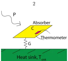
The bolometer concept is ubiquitous in infrared sensor design. The basic setup consists of an absorbing element with heat capacityC which is attached to a heat sink by thin legs which have a combined thermal conductanceG(Fig. 1.1). The heat sink is well thermally sunk so as to maintain a constant base temperature from which the isolated absorbing element’s temperature will deviate. When a power sourceP is turned on, the absorbing element’s temperature rises to a limiting value ofTsink+P/Gwith time constant τth =C/G. A thermometer placed on the island measures this
Figure 1.1: Schematic diagram of a bolometer pixel. A thermometer measures the temperature change associated with a change in incident power P on the absorber with heat capacityC. Heat escapes to the substrate via thin legs with combined thermal conductanceG.
1.1.1
Bolometer modeling
The quantities C,G and the noise equivalent power in a bolometer may be calculated in terms of fundamental dimensions and properties of the device. The heat capacity of a slab of material of massm, densityρand specific heatc is given by
C= mc ρ .
The thermal conductance of a wire with lengthl, cross-sectional areaAand resistivityρis given by
G=ρA l .
Quantized fluctuations in the thermal energy flowing across the legs introduce phonon noise. The phonon noise contribution to the noise equivalent power is given by
NEPphonon=
√ 4kT2G
in units of W/√Hz [13].
1.2
Introduction to superconducting microresonators
1.2.1
Microresonator electrodynamics
True to their name superconducting microresonators have zero resistance for direct currents when cooled below their superconducting transition temperatureTc. This supercurrent is carried by pairs
of electrons, called Cooper pairs, with binding energy 2∆≈3.5kBTc forT Tc [2]. However, for
alternating currents energy may be stored as kinetic energy in the Cooper pairs and may be recovered without loss by reversing the electric field. Thin (10s to 100s of nanometers) superconducting films additionally permit energy to be transferred between Cooper pair motion and the magnetic field, since magnetic fields penetrate below the surface of superconductors a distanceλ, called the London penetration depth, which is typically of order the thickness of the film. This reactive energy flow results in a surface kinetic inductanceLs=µ0λ.
Additionally a dissipative component to the conductivity is present due to the small fraction of electrons not bound up in Cooper pairs, called quasiparticles, which behave as normal electrons (i.e. they do not carry the supercurrent). The presence of quasiparticles and the finite inertia of the Cooper pairs result in a complex conductivity σ(ω) =σ1(ω)−iσ2(ω) as described by the
Mattis-Bardeen theory [10]. Any energy inputE >2∆ which breaks a Cooper pair into quasiparticles will introduce a corresponding perturbation in the complex conductivityδσ. This perturbation may be measured very precisely by constructing a resonant circuit.
1.2.2
Principles of operation
Superconducting microresonator detectors are typically either a quarter-wave transmission line res-onator or a lumped-element circuit. A single coplanar waveguide (CPW) transmission line is coupled to every pixel in the array. The superconducting material is carefully chosen so that the resonators exhibit very low loss in each oscillation; quality factors ofQ∼105 are readily obtainable. Since the
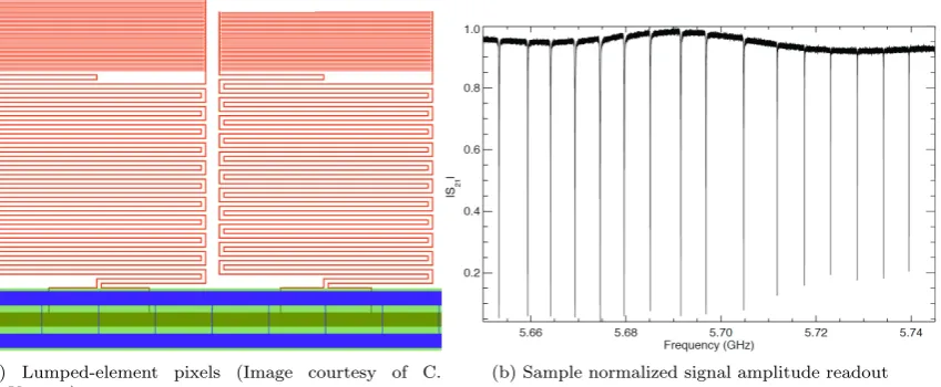
device studied in this paper utilizes the lumped-element pixels, I will focus my discussion on that design. A lumped-element pixel consists of a capacitor and inductor in series which are capacitively coupled to the transmission line (Fig. 1.2a). By varying the capacitor area, the capacitance and thus the characteristic resonant frequency of the pixel may be varied in a controlled manner according to ω= (LC)−1/2.
(a) Lumped-element pixels (Image courtesy of C. McKenney)
[image:11.595.116.541.83.258.2](b) Sample normalized signal amplitude readout
Figure 1.2: (a) An example of the lumped-element design. The interdigitated capacitor, top, can be varied in size to control the resonant frequency of the pixel. In the center, the meandered inductor, which acts as the photon absorber, takes up most of the pixel area. The coplanar waveguide, along which the microwave signal travels, is visible at the bottom. (b) Signal transmission vs. frequency using standard scattering matrix notation. Each dip in transmission indicates attenuation from a resonant pixel coupled to the transmission line.
1.2.3
Frequency multiplexing
By tuning each pixel to a different resonant frequency, multiple pixels may be read out simply by varying the AC frequency on the feedline (Fig. 1.2b). Only this single feedline is required to read out the entire array. Pixels may be engineered to be closely spaced in frequency, in principle allowing hundreds to thousands of pixels coupled to a single feedline. Furthermore, the readout technology required for such large arrays already exists. One example is the CASPER ROACH processing board shown in Fig. 1.3 [4]. One system is currently being used to read out the 32 x 32 pixel ARray Camera for Optical to Near-infrared Spectrophotometry (ARCONS) [11].
1.2.4
Photon absorption
Figure 1.3: A Reconfigurable Open Architecture Computing Hardware (ROACH) board used to read out large superconducting microresonator arrays.
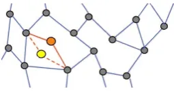
Figure 1.4: Two level systems, in which an atom may quantum tunnel between two local minima in potential energy, are hosted in a thin amorphous surface layer on the crystalline substrate. They introduce excess noise in the position of the resonant frequency in a resonant circuit.
1.2.5
Two level systems
[image:12.595.258.386.288.355.2]1.3
The resonator bolometer
Superconducting microresonators are revolutionary devices but they do not come without limita-tions. They must operate at temperatures T Tc, where the surface inductance dominates. To
operate in the 1 - 4K temperature range, desirable for its simple cooling requirements compared to sub-Kelvin temperatures, superconductors with Tc ∼ 15K must be used. However,
superconduc-tors with such high transition temperatures have short quasiparticle lifetimes [9]. The quasiparticle lifetime, or the time it takes for quasiparticles to recombine once formed, limits the sensitivity of a detector. For constant illumination, a shorter lifetime implies fewer quasiparticles at a given time and thus a smaller signal. Thus microresonators must operate at sub-Kelvin temperatures to remain sensitive.
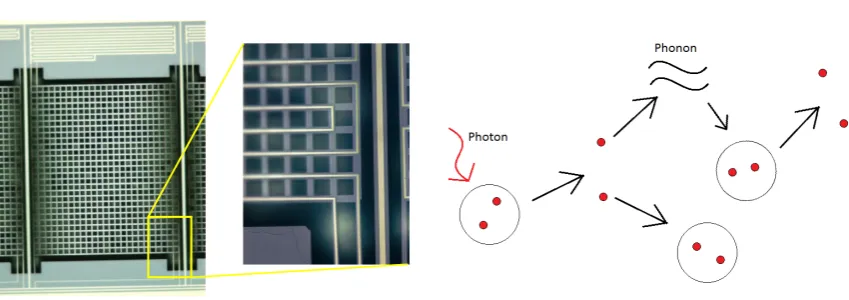
Along with my collaborators at Caltech and NASA’s Jet Propulsion Laboratory I have inves-tigated placing the sensitive portion of the resonator on a thermally insulated island as a way to circumvent this obstacle. In the resonator bolometer, the inductor is placed on the bolometer island, where it acts as both the photon absorber and the thermometer measuring the energy trapped on the island. The rest of the circuit is deposited directly onto the substrate (Fig. 1.5a). This design effectively extends the quasiparticle lifetime because thermal energy released from the recombination of a pair of quasiparticles is trapped on the island, where it may break another Cooper pair (Fig. 1.5b). The magnitude of the signal is thus governed by heat flow from the bolometer island legs to the substrate instead of by the quasiparticle recombination time. In contrast, in a superconducting film deposited directly on the substrate, the emitted thermal energy, or phonon, simply escapes to the substrate, and only incident photons break Cooper pairs.
The resonator bolometer design thus allows for a broad class of superconducting materials to be used in fabrication. It additionally enables a straightforward decoupling of the meander from photon detection; a separate absorber could easily be placed on a bolometer island with a resonator inductor, with the resonator detecting the thermal energy produced by this absorber.
This design has many potential science applications. The ability to operate at temperatures above 1K makes the resonator bolometer attractive for space-based instrumentation because of the greatly simplified cryogenic setup. It is especially suitable for high-background applications such as Earth observation in the far-infrared because of the tunability of the dynamic range enabled by the use of high-Tc superconductors. The investigation into the viability of the bolometric island as a
(a) Resonator bolometer pixel (b) Energy recycling in a resonator bolometer pixel
Figure 1.5: (a) A resonator bolometer pixel. The inductor is on a wire mesh grid released from the substrate and connected to it via six legs (see closeup). The capacitor (top) and the CPW (bottom) are both directly on the substrate. (b) Energy recycling in a resonator bolometer pixel. An incident photon breaks a Cooper pair into its constituent quasiparticles, which quickly recombine. The energy from recombination is emitted as a phonon. Since the phonon is trapped on the isolated island, it is available to break another Cooper pair. Overall, a given input power causes more quasiparticles to exist at a given time than if the sensitive portion of the pixel were not thermally isolated, so that the signal is larger.
1.3.1
Fabrication
In order to begin investigating the feasibility of the resonator bolometer concept, a prototype array was fabricated at NASA’s Jet Propulsion Laboratory (Fig. 1.6). This array consists of a single row of 16 pixels in two frequency bands. The chosen superconducting material is NbTiN, with a Tc of
Chapter 2
Measurement Techniques
2.1
Overview
Several measurements were performed on this prototype array in order to demonstrate its function-ality and characterize it fully. Under dark conditions, when the detector is not exposed to light, the temperature dependence of the resonant frequency and quality factor for several pixels was mea-sured. In addition the noise equivalent power (NEP) was obtained as a function of both temperature and readout power. Under illumination, the response of a pixel to a small change in illumination was measured, as well as the NEP and time constant associated with the time taken for the signal to return to baseline upon removal of the radiation source.
2.2
Measurement setup
See Figure 2.1. The basic measurement is a change in amplitude and phase of a tone of a given frequency after interacting with the pixels of the array. A frequency tone is generated by the microwave source and split, with one branch sent straight to a mixer and the other to a transmission line coupled to each pixel, where absorption from a resonance may occur. The two branches are recombined by the mixer, and the two orthogonal components, which can be thought of as the real and imaginary components of the signal, are low pass filtered before being read in by a data acquisition card and saved to file.
Figure 2.1: Measurement setup. A frequency tone generated by a microwave source is split, with one component traversing the transmission line near the detector pixels, and recombined by a mixer to retrieve orthogonal components of the signal, which are used to calculate amplitude and phase information.
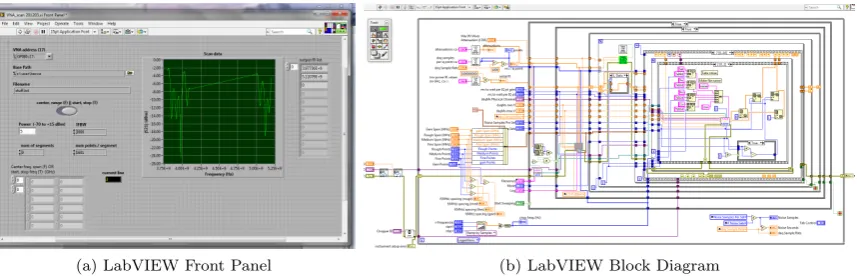
(a) LabVIEW Front Panel (b) LabVIEW Block Diagram
[image:17.595.112.541.483.621.2]2.3
Fitting for the resonant frequency and quality factor
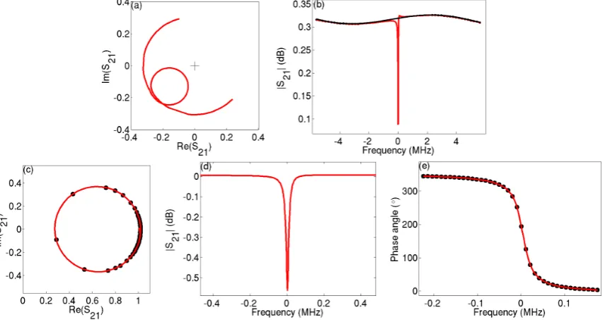
Sweeping over a range of frequencies, one can reconstruct the resonance profile for a given pixel. Using the standard scattering matrix description of the circuit, the transmitted raw data obeys the relation [6]:
S21≡I+jQ=a(f)ej(ωτ+ϕ)
1−Qr Qc
ejφ
1 + 2jQrx
, (2.1)
where the fractional frequency shift x is given by
x= f−fresonance fresonance
. (2.2)
In equation (2.1), a(f) represents the frequency-dependent amplitude of the signal if the reso-nance were absent (the baseline transmission) and ej(ωτ+ϕ)is the cable delay term with ω = 2πf,
τ being the phase shift atf for the cable length present (the cable delay) andϕbeing the phase at zero frequency. Qr = (Q−i1+Q−
1
c )−
1 is the total quality factor with Q
i being the internal quality
factor and Qc being the coupling quality factor, andφ is an arbitrary phase due to wire bonding.
S21 is the fraction of power transmitted. Note that Q, the imaginary part of S21, is distinct from
the various quality factorsQr,Qc andQi.
The first steps in solving for the resonance parametersfr,Qi andQc are to remove the leading
factors: the baseline transmission and the cable delay term. By adequately sampling the frequencies near, but not in, the resonance, the cable delay term ωτ +ϕmay be fit to a line and the baseline transmissiona(f) may be fit to a high degree polynomial (Fig. 2.3 (a), (b)).
Next, the resonance is fit to a circle in the IQ plane (Fig. 2.3 (c)) according to the equation
S21= 1−
Qr
Qc
ejφ 1 + 2jQrx
Chapter 3
Dark Measurement Results
The measurements taken can be neatly divided into dark measurements, where the array and cryostat windows were covered to keep optical radiation from reaching the array, and measurements under illumination, where a controlled radiation source was placed in front of the cryostat window to illuminate the detector. Both types of measurement are of interest for characterizing this array; the dark measurements offer a glimpse into the operating capabilities under very low light conditions and allow the most fundamental and characteristic noise sources to dominate and be studied. In contrast the illuminated measurements are more similar to how this array might be used for science so they provide a more concrete picture of the array’s potential performance. I will begin by presenting the dark measurement results and later compare these to the illuminated measurement results.
3.1
Temperature dependence
The simplest experiment to carry out is to vary the temperature of the device and record the changes in the resonance. A detector pixel responds to changes in temperature and changes in incident radiation similarly since both processes result in additional Cooper pair-breaking energy in the inductor. Thus we expect to see both the resonant frequencyfr and the quality factorQi of the
resonance varying with temperature, which was observed (Fig. 3.1). Also shown in the figure is the best fit of a theoretical model based on the Mattis-Bardeen theory of superconductivity. The model is derived in Appendix A. To fitfr(T), the superconducting transition temperature Tc was allowed
to vary; Tc = 13.7K yielded the best fit. Q−i1(T) depends both onTc and the kinetic inductance
fractionα, defined as the ratio of the kinetic inductanceLk to the total inductanceLk+Ls, whereLs
is the temperature-invariant geometric inductance. For this fit we fixedTc at the value determined
from the fit tofr(T) and variedα. α= 0.55 gave the best fit.
(a) Fractional frequency shift vs. temperature (b) Quality factor vs. temperature
Figure 3.1: (a) Fractional frequency shift x vs. temperature. The data points are plotted in red, with the fit from Mattis-Bardeen theory (Appendix A) in blue. The fit is a best fit line; the superconducting transition temperatureTcwas allowed to vary to find the curve which best matched
the data. The shown curve corresponds toTc = 13.7K, which is the value the material was designed
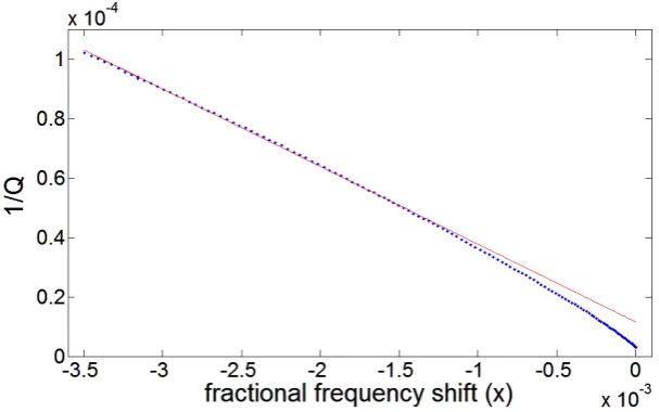
to have. (b) Inverse quality factor vs. temperature. The theory predicts thatQ→ ∞asT →0. In this and other superconducting microresonator-based devices however, Q is observed to approach a finite maximum; this is due to other sources of dissipation, including TLS (Section 1.2.5) and radiation into free space [15]. The gap in the data near 2.2 K is the lambda point of liquid helium, where it transitions from superfluid to normal liquid and the associated large change in heat capacity causes a jump in the temperature.
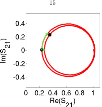
[image:21.595.172.476.454.644.2]Figure 3.3: To measure a signal change, resonances sampled before and after a change in incident power are compared. The resonant frequency fr before the change is at a different position after
the change; the fractional frequency shiftxis thus (frold−frnew)/frnew. The signal change in the
dissipation direction is also shown.
3.2
Response
With the basic behavior of the resonances understood, the next step was to look toward the mea-surements necessary to find out the sensitivity of the array. The sensitivity depends both on the magnitude of the response of the resonator to a small change in the incident power and the ran-dom fluctuations, or noise, in the resonator properties measured. If the power change results in a response so small that it cannot be distinguished from the random fluctuations, then the detector is not sensitive enough to observe that change. More precisely, the sensitivity for long wavelength detectors is usually given as the noise equivalent power, defined for noiseSxx and responseR as
N EP = √
Sxx
R . (3.1)
Thus accurate measurements of both the response and the noise are necessary to estimate the NEP. Signal changes are measured by comparing a resonance before and after a small change in the incident power. Because both reactive and dissipative changes occur, either or both of these changes may be measured independently to infer the change in incident power. Changes in the resonant frequency (reactive) are along the resonance loop and dissipation changes are perpendicular to it (Fig. 3.3). The response is significantly larger in the frequency direction as a consequence of superconductivity theory. This makes the frequency direction less susceptible to electronic noise; for this reason, we focus on the response and noise measurements in the frequency direction only. The signal change produces a response in the form of a fractional frequency shiftx, given by Eq. (2.2). Note that in a system where this detector is used for science applications, both directions may be used.
the mechanism is straightforward; a change in the incident power causes changes in the resonance as described above. In the latter case, small temperature changes serve as the effective signal. These may be converted to equivalent changes in incident power by G, the thermal conductance of the bolometer island legs:
G∆T = ∆P. The response under dark conditions is thus
R= ∆x G∆T.
3.2.1
Thermal conductance calculation
x/∆T, the response to temperature changes, is readily calculated as the derivative of the curve in Fig. 3.1a. The other necessary quantity is the thermal conductance Gof the bolometer island legs. It is known empirically thatGexhibits a roughlyT3 dependence [1]. From the phonon NEP expression given in Section 1.1.1 and Eq. (3.1), we can solve forG:
G=4kBT
2(∆x/∆T)2
Sxxphonon
whereSphonon
xx is the phonon contribution to the total noiseSxx. Measurements of the phonon noise
(see Section 3.3.3 below) fit to aT3power law yield, in nW/K,
G≈0.3T3.
3.2.2
Results
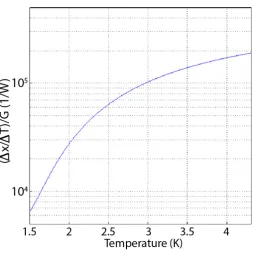
The response is shown as a function of temperature in Fig. 3.4. Importantly, there is well over an order of magnitude difference between the response at 1.5 K and at 4 K, suggesting that the lowest temperatures will not yield the optimal sensitivity.
3.3
Noise
3.3.1
Data collection and processing
Figure 3.4: Calculated response fromG= 0.3T3nW/K.
for reasons stated above (Sec. 3.2). From the initial scan of the resonance, a mapping between the generator frequencies and the points on the resonance loop is made, and the fractional frequency shiftxfor each point is calculated (Eq. (2.2)).
Next, the power spectral density of the time stream of data is computed. The power spectral density quantifies the power carried by each frequency component of a stochastic process (in this case, the noise data stream) and is typically given in Watts/Hz. This is normalized by dividing by the total power in the signal to yield the fractional frequency noiseSxxin (Hz)−1.
3.3.2
Noise sources
Figure 3.5: Noise at resonance. Each data point in the green spread is mapped to a frequency using the fit to a frequency scan over the resonance (black points).
[image:25.595.153.491.361.649.2]3.3.3
Dark noise results
In practice, signals varying with frequencies above the bolometer roll-off cannot be observed with this detector because the averaging effect of the bolometer time constant will reduce the signal. Thus the frequencies of interest for operation are∼ 150 Hz and below. Extraneous noise from thermal drift and excess noise exhibited by our cryogenic amplifier dominate at very low frequencies. In the future, these can be greatly reduced with a new amplifier and a thermally controlled sample stage. For this measurement however, the value ofSxxused to calculate the NEP is an average of the data
points within the green box in Fig. 3.6, excluding the electronic noise spikes. This average noise is plotted vs. temperature in Fig. 3.7. A clear minimum is visible at∼2.5 K; to either side, the two most important noise sources dominate. At high temperatures, the phonon noise dominates; it is given by
Sxxphonon= 4kBT
2(∆x/∆T)2
G .
The plotted phonon noise curve is a best fit of this equation to the data, with G as a variable parameter. G = 0.3T3 nW/K yields the best fit; thus this was the dependence chosen for the
response calculation (section 3.2).
At the low temperature end, the TLS noise dominates due to its T−2 dependence. The exact proportionality constant for this dependence was also chosen for its fit to the data; thus
SxxTLS= 3∗10
−19K2/Hz
T2 .
Chapter 4
Measurements under illumination
Up to this point I have discussed only the dark measurements. While most of the procedure remains the same for the corresponding measurements under illumination, particularly the data processing, the experimental setup changes significantly with the addition of an external light source. In this chapter I will explain some of these extra procedural challenges and present the results in comparison with the corresponding dark measurement.
4.1
Optical response measurement
When light is allowed into the cryostat, a change in the power radiated by an optical source leads to changes inx. In this case the response is simply
R= ∆x ∆P.
The changes ∆P were produced by placing a chopper wheel between a voltage-controlled black-body and the cryostat window (Fig. 4.1). The chopper wheel was placed behind a sheet of room-temperature absorbing material with a small hole to define the aperture. As the chopper wheel spun, it alternately blocked and passed light from the blackbody behind it, producing an approxi-mately square wave signal of amplitude ∆P. The corresponding frequency changes were recorded as a function of operating temperature and the results are presented in Fig. 4.2.
4.2
Time Constant
Figure 4.1: Setup for the optical response measurement. Light from a blackbody held at a fixed temperature is modulated by the rotation of the chopper wheel. An aluminum plate covered in an absorbing material placed in front of the chopper with a small hole for the aperture ensures that off-axis radiation entering the cryostat comes from a homogeneous source.
[image:29.595.199.452.402.653.2]Figure 4.3: Setup for the time constant measurement. A terahertz radiation source was used to ensure that the transitions between low and high intensity were fast compared to the bolometer time constant.
(a) Response to a pulse of THz radiation (b) Fit to the response decay
Figure 4.4: (a) Responses at low and high operating T to the THz pulse show the substantial difference in the magnitude of the response at these two temperatures. (b) The rise and decay curves may be fit to an exponential (black curves) to estimate the time constant. τ4K = 475µs and
τ1.5K= 365µs.
radiation source was used in place of the blackbody and chopper setup to ensure that sharp square pulses were produced when compared to the bolometer time constant (Fig. 4.3).
Sample pulses are shown in Fig. 4.4a. The difference in response between 1.5 K and 4 K is clearly visible. Also evident are the exponential rise and decay of the frequency shift. Fitting the decay curves to an exponential function (Fig. 4.4b) yields τ4K = 475µs and τ1.5K = 365µs; these
[image:30.595.114.539.289.434.2]Figure 4.5: Noise plots for a single pixel at a constant temperature (∼ 3 K). While the overall structure is similar, the noise under illumination is higher below the phonon noise roll-off, reflecting the presence of photon noise.
4.3
Noise under illumination
Fig. 4.5 compares two noise plots taken at the same temperature for the same pixel under dark and illuminated conditions. Evidently the structure is the same; both measurements clearly exhibit low frequency thermal instability noise, a phonon noise roll-off between 102and 103 Hz, and in this case
TLS noise rolled off by the resonator ring-down time (Appendix B) at high frequencies. However, in the illuminated case the noise is higher below the phonon noise roll-off; this reflects the addition of photon noise, which has no intrinsic spectral dependence but which is rolled off by the detector response.
When we again average the noise around 150 Hz over multiple temperatures, we see the added photon noise contribution in the optical data when compared with the dark data (Fig. 4.6). As-suming a constant photon NEP, the photon noise may be calculated:
Figure 4.6: Noise vs. temperature at 150 Hz. The red data points are the noise under illumination while the blue data points are under dark conditions. Adding a constant photon NEP modulated by the response of the detector and added to the phonon and TLS noise determined from the dark data produces good agreement with the data forT >2.5K.
NEPphoton= 8*10−15W/Hz1/2 produces the best fit to the data. The photon noise is added to the
phonon and TLS noise as fit from the dark data.
4.4
Noise equivalent power
The noise equivalent power (NEP) in terms of the fractional frequency noise and response is
N EP = √
Sxx
R .
The dark and illuminated NEP are plotted together with the photon NEP in Figure 4.7. A clear minimum is present in the dark NEP around 3 K and to some extent also in the illuminated NEP. The upward trend as temperature decreases reflects the diminishing response, while in the opposite direction phonon and photon noise dominate.
Figure 4.7: Noise equivalent power under dark and illuminated conditions as compared to the calculated photon NEP. A NEP minimum is established around 3 K. The discrepancy between the photon NEP and the measured NEP under illumination is currently being investigated.
Chapter 5
Conclusion
The measurements presented here form a comprehensive characterization of the resonator bolometer array and point towards several avenues of further research. Design changes have been proposed which would improve the device performance. For example, depositing the capacitor directly onto the silicon substrate instead of on a layer of silicon nitride should substantially reduce the TLS noise. Additionally, other superconducting microresonator detector projects have begun to engineer the resonances at much lower frequencies in order to eliminate the need for an analog mixer. Removing this analog component not only reduces complexity but significantly reduces cost and removes a potential source of electronic noise from the system. Finally, investigations into increased optical coupling will help ready this device for science applications.
Appendix A
Expressions for
f
r
(
T
)
and
Q
i
(
T
)
from Mattis-Bardeen theory
The Mattis-Bardeen theory of the anomalous skin effect in superconductors [10] may be used to derive the behavior of the resonance as the superconductor’s temperature is varied.
A.1
Temperature dependence of
f
rGiven conductivityσs=σ1−iσ2, the superconducting resistivity is
ρs≡
1 σs
=σ1+iσ2 σ2
1+σ22
. The superconducting resistance is thus
Rs=
σ1
σ2 1+σ22
RN
where RN is the resistance in the normal state. Likewise, the superconducting inductance is given
by
ωLs=
σ2
σ2 1+σ22
RN
whereω is the angular frequency. The resonant frequency of an LC circuit is
2πfr=ωr=
1 √
LC. Letf0 be the resonant frequency of the circuit at 0K. Then
x≡ fr−f0 f0
=fr f0
−1 =
s
(LrC)−1
(L0C)−1
−1 =
r
L0
Lr
=
s
σ20
ω0(σ210+σ
2 20)
ωr(σ12r+σ
2 2r)
σ2r
−1.
Because we are dealing with frequency changes on the order of a few thousandths off0 (i.e. a few
MHz),ωr/ω0 ≈1. Also, forT Tc, σ2 σ1, so σ21+σ22 ≈σ22. Using these approximations, we
have:
x≈
rσ
2r
σ20
−1.
σ2is related to the temperature by
σ2(ω)
σn
= 1
~ω
Z ∆+~ω
∆
dE E
2+ ∆2−
~ωE
√
E2−∆2p
∆2−(E−
~ω)2
[1−2f(E)], (A.1)
where σn is the normal state conductivity, ∆≈3.5kBTc is half the Cooper pair binding energy,ω
is the angular resonant frequency andf(E) is the distribution function for quasiparticles, given by f(E) = 1/(eE/kT + 1) in thermal equilibrium.
A.2
Temperature dependence of
Q
iThe internal quality factorQi is the ratio ofωtimes the kinetic inductanceLk to the resistanceRs
in the circuit. The kinetic inductance fraction α≡Lk/Ls. Using the equations forRsand ωLs in
section A.1, we can expressQi as a function ofσ1 andσ2:
Qi =
ωLk Rs = 1 α ωLs Rs = 1 α σ2 σ1 . σ2is given by Equation (A.1), while
σ1(ω)
σn = 2 ~ω Z ∞ ∆ dE E
2+ ∆2+
~ωE
√
E2−∆2p
(E+~ω)2−∆2[f(E)−f(E+~ω)]
Appendix B
Resonator ring-down time
derivation
The total quality factorQr is given by:
Qr=
ω0
P
whereω0= 2πf0is the angular resonant frequency, = 12LI2is the energy stored in the resonance
andP =12I2Ris the power dissipated. Plugging in forandP yields:
Qr=
ω012LI2 1 2I
2R =
ω0L
R
The attenuation can be obtained by solving the equation of motion for an RLC circuit and is equal to 2RL. Then we have:
attenuation = R 2L =
ω0
2 R ω0L
=ω0 2
1 Qr
= 2πf0 2Qr
= πf0 Qr
The resonator ring-down time τres is defined as the inverse of attenuation, so, in terms of
quan-tities easily found from fitting resonances,
τres=
Qr
πf0
. (B.1)
τres can also be expressed in terms of the bandwidth ∆f by substitutingQr= ∆f0f:
τres=
1 π∆f.
Appendix C
HFSS modeling calculations
An accurate NEP under loading can only be determined if the optical power reaching the detector is well known. This requires knowledge of both the absorption of the filters in front of the detector and the spectral dependence of the absorption of the detector itself. The former is provided by specification sheets for the filters, but the latter must be measured or modeled. In order to confidently report the amount of radiation absorbed by the detector, we have modeled the absorption of a single pixel. Details of the methodology are reported here.
C.1
Description of circuit
See section 1.3.1.
C.2
Analytic solution to simplest case
[image:38.595.207.441.571.653.2]The simplest approximation treats the meandering inductor as a uniform 80 Ω sheet resistance on one surface of the silicon substrate in free space (see Fig. C.1). The Si substrate has a thickness of l = 500 µm. Standing waves can occur in the silicon. Maximum transmission occurs when the
substrate thickness is an odd integer multiple of a quarter of a wavelength. Minimum transmission occurs when the substrate thickness is an even integer multiple of a quarter of a wavelength. To find the frequencies of minimum and maximum transmission, we evaluate:
nλ 4 = n 4 c ν√ where λ/4 =l= 500µm andSi= 11.9. Solving yields
nν=n∗4.35∗1010Hz.
In the case that n is even, we are dealing with half-wavelength multiples, so the magnitude of the voltage is the same at either end of the silicon section. This means we can eliminate it from the circuit. The simplified circuit is free space in series with free space and a 50 Ω sheet resistance to ground in parallel. The equivalent impedance for the parallel section is
1
1 50Ω +
1 377Ω
= 44.1 Ω.
And the reflection coefficient for the transition between free space and this load is
Γ1 2λ=
377−44.1
377 + 44.1 = 0.79.
In the case that n is odd, the equivalent impedance of the Si section plus load (free space in parallel with 50 Ω sheet resistance) isZ2
Si/Zload, so that the reflection coefficient is
Γ1 4λ=
377−(377/√11.9)2/44.1
377 + (377/√11.9)2/44.1 = 0.16.
Bibliography
[1] Neil W. Ashcroft and N. David Mermin. Solid State Physics. Harcourt College Publishers, 1976.
[2] J. Bardeen, L. N. Cooper, and J. R. Schrieffer. Theory of Superconductivity. Physical Review, 108(5):1175–1204, 1957.
[3] R. Barends, H. L. Hortensius, T. Zijlstra, J. J. A. Baselmans, S. J. C. Yates, J. R. Gao, and T. M. Klapwijk. Contribution of dielectrics to frequency and noise of NbTiN superconducting resonators. Applied Physics Letters, 92(22), JUN 2 2008.
[4] Collaboration for Astronomy Signal Processing and Electronics Research. ROACH, February 2012. https://casper.berkeley.edu/wiki/ROACH.
[5] P. K. Day, H. G. LeDuc, B. A. Mazin, A. Vayonakis, and J. Zmuidzinas. A broadband su-perconducting detector suitable for use in large arrays. Nature, 425(6960):817–821, OCT 23 2003.
[6] Jiansong Gao. The Physics of Superconducting Microwave Resonators. PhD thesis, California Institute of Technology, 2008.
[7] Jiansong Gao, Miguel Daal, John M. Martinis, Anastasios Vayonakis, Jonas Zmuidzinas, Bernard Sadoulet, Benjamin A. Mazin, Peter K. Day, and Henry G. Leduc. A semiempirical model for two-level system noise in superconducting microresonators. Applied Physics Letters, 92(21), MAY 26 2008.
[8] Jiansong Gao, Jonas Zmuidzinas, Benjamin A. Mazin, Henry G. LeDuc, and Peter K. Day. Noise properties of superconducting coplanar waveguide microwave resonators.Applied Physics Letters, 90(10), MAR 5 2007.
[10] D. C. Mattis and J. Bardeen. Theory of the Anomalous Skin Effect in Normal and Supercon-ducting Metals. Physical Review, 111(2):412–417, 1958.
[11] Sean McHugh, Benjamin A. Mazin, Bruno Serfass, Seth Meeker, Kieran O’Brien, Ran Duan, Rick Raffanti, and Dan Werthimer. A readout for large arrays of microwave kinetic inductance detectors. Review of Scientific Instruments, 83(4), APR 2012.
[12] D. C. Moore, S. Golwala, B. Bumble, B. Cornell, B. A. Mazin, J. Gao, P. K. Day, H. G. LeDuc, and J. Zmuidzinas. Phonon Mediated Microwave Kinetic Inductance Detectors.Journal of Low Temperature Physics, 167(3-4, Part 1):329–334, MAY 2012. 14th International Workshop on Low Temperature Particle Detection (LTD), Heidelberg Univ, Kirchhoff-Inst Phys, Heidelberg, GERMANY, AUG 01-05, 2011.
[13] P. L. Richards. Bolometers for infrared and millimeter waves. Journal of Applied Physics, 76(1):1–24, 1994.
[14] A Wallraff, DI Schuster, A Blais, L Frunzio, RS Huang, J Majer, S Kumar, SM Girvin, and RJ Schoelkopf. Strong coupling of a single photon to a superconducting qubit using circuit quantum electrodynamics. Nature, 431(7005):162–167, SEP 9 2004.