1
Sono-electrodeposition transfer of micro-scale copper
patterns on to A7 substrates using a mask-less method
Albert Serrà a,*, Simon J. Coleman b, Elvira Gómez a, T.A. Green c, Elisa Vallés a, Joan Vilana a, Sudipta Roy c
a
Grup d’Electrodeposició de Capes Primes i Nanoestructures (GE-CPN), Departament de
Química Física and Institut de Nanociència i Nanotecnologia (IN2UB), Universitat de
Barcelona, Martí i Franquès 1, E-08028, Barcelona, Spain.
b
School of Chemical Engineering and Advanced Materials (CEAM), Merz Court, Newcastle
University, Newcastle upon Tyne, NE2 7RU, UK.
c Department of Chemical and Process Engineering, University of Strathclyde, James Weir
Building, 75 Montrose Street, Glasgow, G1 1XJ, UK.
Corresponding Author: Albert Serrà
Grup d’Electrodeposició de Capes Primes i Nanoestructures (GE-CPN), Departament de Química
Física and Institut de Nanociència i Nanotecnologia (IN2UB), Universitat de Barcelona, Martí i Franquès 1, E-08028, Barcelona, Spain
E-mail: [email protected] Fax: +34 93 4021231 Tel: +34 93 4039241
2
ABSTRACT
A patterned anode tool was used to transfer electrodeposited microstructures on to an un-patterned A7 sized cathode by maintaining very narrow separation (300 µm) between the two electrodes and agitating the fluid in the inter-electrode gap by ultrasonic means. A non-acidic copper solution with a low content of metal ions and additives was used. Limiting current experiments were initially performed to demonstrate that improved and uniform agitation could be maintained within the inter-electrode gap at relatively low ultrasonic powers of 5 to 30 W L-1. The best pattern definition was obtained at a US power of 5 W L-1 and a current density of 20 mA cm-2. Importantly, the results obtained were comparable to those obtained by conventional through-mask plating. A single anode tool could be used to pattern up to five substrates, substantially minimising the amount of lithographic processing required. These results suggest that the proposed technique is a useful mask-less microfabrication process for pattern transfer on to large substrates.
3
1.
INTRODUCTION
Copper electrodeposition is a key fabrication technique in micro- and nano-fabrication and is routinely employed to manufacture microelectronic, optoelectronic and MEMS devices [1-4]. While thin films of copper can be deposited using a variety of ‘dry’ techniques such as PVD and CVD, ‘wet’
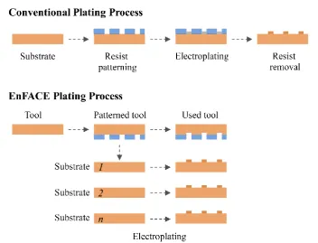
methods based on electrodeposition are generally preferred for most applications [5]. In microfabrication, the technique of through-mask plating [6] is typically employed to form patterned metal films on substrates. This typically involves coating the substrates with a photoresist and then patterning it using conventional photolithography. This photoresist then acts as a mould to define the areas of electroplating. Importantly, through mask plating is a batch processing technique where many microstructures are formed in parallel. More recently, techniques based on patterned electrodeposition using conformal masks have been developed [7,8] which allow more complex 3D structures to be formed.
A number of alternative techniques [9-11] employing direct-writing or mask-less methods have also been developed to electrodeposit micro-structures, and these have the advantage of reducing the costs and limitations associated with conventional lithography. However, while these approaches are capable of high resolution, they are serial fabrication methods and therefore less suitable for the volume production of micro-devices. The electrodeposition of nano-structures can also be perfomed
via through-mask plating using e-beam lithography, but these are more conveniently prepared using various nano-templates [12]. However, in recent years, many strategies using soft-templates like micro-emulsions [13,14], assembly of micelles [15], self-assembled monolayers [16], have been proposed to fabricate nano-structures electrochemically, thereby avoiding the use of the classical hard-templating.
4
a substrate [18-21]. As shown in Figure 1, the technique advocates the use of a patterned masked electrochemical tool which is positioned close to the substrate, and a current is then imposed to transfer the tool pattern on to the substrate [18-21]. The process does not avoid the use of a physical mask completely, but has the advantage that a single patterned tool can be used to electro-etch or electrodeposit many substrates. Compared to the standard technique of through-mask plating (Figure 1) where each substrate has to be individually patterned with a resist mask [4, 6] this results in significant reduction in material usage, processing time and cost.
The proposed technique does, however, require careful control of the reactor design, and a narrow inter-electrode gap of less than 500 µm [17-20]. The thin gap between the electrodes can limit mass transport and anodic or cathodic gas evolution resulting in bubble formation and retention has also been recognised as issue [20-21] which could limit its potential use. In addition, it has been shown that an acceptable deposition rate requires high and uniform mass transport in the inter-electrode gap. Similarly, good feature definition which exhibit minimum current spreading requires the use of a narrow and repeatable gap and a low conductivity (i.e. acid-free) electrolyte [17-20]. Therefore, in order to fully exploit the potential of the technique, a method to provide adequate mass transfer between the two closely spaced electrodes is essential.
5
having much wider feature than on the anode tool. A final concern is that the cavitation bubbles formed at these high powers can be retained in the gap and degrade the pattern definition.
In this paper we describe the electrodeposition of patterned copper on to A7 sized copper plates at relatively low ultrasonic power (typically 5 – 30 W L-1) in an attempt to minimise some of the adverse effects identified in earlier work [24]. In addition, a non-acidic bath with a low content of additives is used, which has previously been shown to produce copper deposits with characteristics compatible with the printed circuit board industry [25]. This is in contrast to the earlier study [24] which did not employ any additives and typically employed much higher ultrasonic powers. The results reported here are directly compared with these previous findings and also against those obtained using the classical through-mask plating process.
2.
EXPERIMENTAL
2.1.
Chemicals and Materials Used
It has been previously demonstrated [19] that the EnFACE process requires an acid-free bath and recently [25] it has been shown that low concentrations of commercial additives, which are normally used to plate printed circuits boards (Copper Gleam HS 200 – Dow Electronic Materials), can be used effectively with these electrolyte. The electrolyte solution used in experiments contained 0.1 M CuSO4, 5 mL L-1 of Gleam HS-200B, 2.5 mL L-1 of Gleam HS-200A and 35 µL L-1 of HCl. The Gleam HS-200B additive is a large molecular weight polyoxy-alkyl compound which functions as a carrier/suppressor. Similarly, the HS-200A additive is an unidentified organosulfur species which acts as a brightener/accelerator. The electrolyte solutions were prepared with deionized water with a resistivity of 13.7 MΩ cm.
6
cathode plates were manually polished with #1200, #2000 and #4000 grit SiC paper. They were then cleaned in a Decon 90 solution, rinsed with deionised water and dried thoroughly using nitrogen.
2.2.
Experimental Apparatus
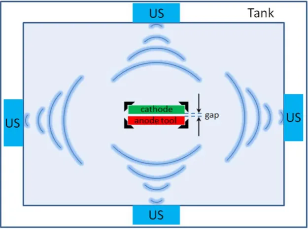
Electrochemical experiments were carried out in an 18 L ultrasonic tank reactor with transducers
mounted on the sidewalls and bottom of the tank (Figure 2). Special PVC electrode holders were used to mount the large A7 size substrates and tools in the tank with a narrow and uniform
inter-electrode gap.A detailed description of the tank, the PVC holders, and their methodology of loading
and unloading them has been provided in detail in Reference 24, and is therefore not described here. A standard calorimetric method was used for measuring and calibrating the ultrasonic power prior to the copper deposition experiments [26]. The electrodeposition experiments were of two different varieties: (1) limiting current experiments to determine the degree of mass transport induced by US agitation, and (2) pattern transfer experiments to determine the thickness, surface roughness and feature dimensions of the electrodeposits. All the electrochemical experiments were carried out under galvanostatic conditions using a DC power supply (Thurlby Thandar PL320).
2.3.
Limiting Current Experiments
7
measured at different positions. These are shown as regions B and F in Figure 1S. In the present work a power range of 5 W L-1 to 30 W L-1 is used.
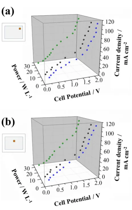
For each experiment the A7-sized electrodes were initially loaded into Perspex holders (Figure 1S). The limiting current experiments at each US power were then carried out by applying current densities of j = 10 - 120 mA cm-2 for 30 seconds and measuring the overall cell potential, E. This method of estimating the limiting current is often employed in industrial situations when the use of a reference electrode is impractical or impossible [33]. The limiting current density (jlim) was obtained directly from the plateau region of the j-E plots. Each limiting current experiment was repeated three times and carried out individually at different positions. During these experiments the remainder of the cathode substrate was masked with protective layer of spray-on photoresist. The anode in these experiments was an un-patterned A7 copper plate, and the inter-electrode gap was 1.5 mm.
It should be noted that the limiting current region can be affected by several factors such as the occurrence of secondary reactions, variations in area during the metal deposition, and the prevailing current and potential distributions [33]. Therefore, a clear and well-defined plateau is often not obtained. Recently, significant distortions in the polarisation data have been observed for narrow electrode gaps in a parallel plate configuration [31]. However, it has been shown [24] that a limiting current density can still be estimated from the experimental data, and this can then be used to assess the degree of agitation within the gap.
2.4. Pattern Electrodeposition Experiments
8
linear features were fabricated using a standard dry film photoresist and patterned using photolithography (Figure 3S).
The anode tool with the large square features was prepared according to Figure 2S(b).Firstly, 10 x 10 mm2 areas were masked off using adhesive copper tape. Next, a liquid film resist (PRP Positive Photoresist, Electrolube) was sprayed over the entire surface and cured with an air dryer for 10 minutes. The squares of adhesive copper tape were then removed and the photoresist cured again in an oven at 50 ºC for 20 minutes. Finally, the plate was rinsed in deionized water and dried thoroughly with a N2 gun.
The anode tool with linear micro-scale features was fabricated according to Figure 3S. Firstly, the copper plate was cleaned with isopropanol and dried thoroughly with N2. A 35 μm thick layer of a dry-film resist (E9230, Eternal Chemical Company Ltd.) was then laminated on to the copper plate at a temperature of 110 ºC. A photo-mask with the desired linear pattern was then placed over the resist layer which was then exposed for 15 seconds in a UV exposure unit. The resist was then developed for 13 minutes at 30 oC in a standard K2CO3 developer (Chestech) followed by rinsing in DI water and N2 drying. Note that for the experiments employing conventional through-mask plating the dry film resist processing was applied directly to the cathode plate. It was observed that the electrolyte solution did not always penetrate the fine features of the dry-film resist, which can lead to un-plated areas. To minimise this effect, the substrates were immersed in a 0.5 wt% SDS surfactant solution just prior to each experiment.
Deposited features on the A7 copper plates were initially characterised using a confocal microscope. A 3D optical surface metrology system (Leica DCM 3D) was used to determine the thickness and roughness of the transferred copper patterns. Surface roughness is reported as Ra (arithmetical mean of the absolute values of the average 2D profile departures) or Sa (arithmetic mean height of the 3D surface profile).
9
3.1. Limiting current experiments:
The current-potential data gathered for the limiting current experiments is shown in Figure 3. As can be seen in the figure, there is no clear plateau, and this affects the estimation of the limiting current. However, the data are similar to those observed previously for sono-electrodeposition, and it was shown [22-24, 31] that that limiting current could still be determined in the pseudo-plateau region. Adopting the same procedure used previously [31] the limiting current densities at lower power are shown in Table 1. The limiting current for the two positions (F and B) ranges from 40 – 70 mA cm-2 which compares to a value of 25 mA cm-2 in the absence of US agitation. According to the literature [30-32] such an enhancement in the limiting current density with increasing ultrasonic power is expected.
The diffusion layer thickness, δ, can be calculated from the limiting current as follows:
𝛿 =𝑛 · 𝐹 · 𝐷 · 𝑐𝑏
𝑗lim (1)
where F is the Faraday constant, n is the charge on the electroactive species, D is its diffusion
coefficient and cb is its bulk concentration. The values of δ shown in Table 1 are calculated from equation 1 assuming a value of D = 7.07 x 10⁻⁶ cm2 s-1 for copper ions [34]. As can be seen in Table 1, increasing the ultrasonic power increases the limiting current, which can be attributed to the cavitation and/or micro and macro-streaming effects [30]. Notably, the limiting current at the two different locations (B and F) are nearly identical, which means that the material transfer to these regions is similar during sono-electrodeposition.
10
one finds that mass transfer is indeed enhanced at higher powers. For example, the diffusion layer thickness for 40 W L-1 and 60 W L-1 were 17 and 15 µm, respectively [24]. This can be compared to values of 34 µm (5 W L-1) and 27 µm (10 W L-1) in the current study.
The above data reveal that even relatively low ultrasonic powers can provide sufficient agitation to attain the required transport to and from the electrode surface, even in the central part of an A7 plate in a narrow electrode-gap configuration. However, the value of limiting current will be lower when the inter-electrode gap is 0.3 mm as versus 1.5 mm. For the former case, the onset of limiting current can only be inferred indirectly by a drop in current efficiency and/or increase in surface roughness. The recommended current density for copper plating in industry using these additives is typically 10 - 20 mA cm-2 [25]. The current findings therefore support that these values are achievable for sono-electrodeposition on A7 substrates with a narrow inter-electrode gap.
3.2. Transfer of Centimetre Features
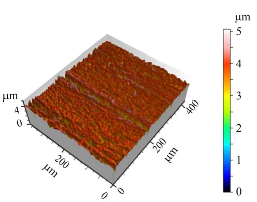
Sono-electrodeposition experiments employing the maskless technique were initially carried out using a patterned tool containing an array of 10 x 10 mm squares. The process was then characterised by analysing the current efficiency, feature size, deposit uniformity and roughness. Before this was performed, an analysis of the surface roughness of the manually polished A7 substrates was obtained as a baseline (Figure 4). These measurements indicated that, prior to electrodeposition, the polished copper substrates typically had an average surface roughness of Ra = 160 nm and Sa = 216 nm.
11
The results in Table 2 indicate that the total surface area, Af, and average lengths, Lf, of the plated features on the cathode were generally larger than the anode feature area. This arises from the current
spreading effect and reflects both variations in the electrode gap across the substrate (typically 40
µm) and also the prevailing current distribution between the electrodes [19-21]. The amount of spread observed at 5 W L-1 and 10 W L-1 was 0% and 10%, respectively. This is significantly lower than value of 14% observed earlier for deposition at 30 W L-1 [24]. The increase in feature dimensions with increasing US power was observed in both this study and the earlier study. This may reflect an ultrasonic enhancement of current spread, but increased damage/delamination of the photoresist on the anode tool at higher powers which increases the effective feature size cannot be ruled out [24].
The current efficiency, , for copper electrodeposition is also shown in Table 2. This was estimated using the expression:
𝜀 = 𝑑 · 𝑛 · 𝐹 · 𝜌 · 𝐴𝑓
𝐴𝑝· 𝑗 · 𝑡 · 𝑀 (2)
where d is the measured average thickness, n is the number of electrons, F is the Faraday constant, ρ is the density of copper, Af is the actual plated area on cathode, Ap is the exposed area on the anode tool, j the current density, t is the deposition time and M is the atomic weight of copper. Figure 5a
indicates that the average thicknesses of the deposits were approximately d = 2.6 - 4.4 µm (Table 2), resulting in a current efficiencies between 85% and 96%. In an earlier study [24] current efficiencies approaching unity were observed at the same current density but with higher US powers and without additives. However, the difficulties in estimating the exact dimensions of the electrodeposited pattern results in errors in the current efficiency of 10 – 20% [24] so these differences may not be significant. More recent work [25] performed with a similar concentration of additives but without US agitation resulted in current efficiencies of 85 - 94% which are in good agreement with the present results.
12
thickness distribution was observed in the earlier study at higher US powers [24]. This is due to the prevailing current distribution between the electrodes, but may also reflect variations in the inter-electrode gap which change the amount of current spread. Finally, the thickness variation across the substrate tended to be lower at the lowest US powers.
As can be seen in Figure 5b the average surface roughness (Sa) is generally higher at the corners than at the centre at all US powers. In part this may be due to the increased deposit thickness at the edges, and an earlier study [20] without US agitation showed a strong development in copper roughness with deposit thickness. Additionally, there appears to be a small reduction in deposit roughness as the US power increases but the trend is relatively weak. In a previous study [24] performed at higher US power (with no additives) there was a similar decrease in roughness as the power was increased from 30 W L-1 to 40 W L-1. At 60 W L-1 the roughness increased again due to cavitation induced pitting.
Some of the observed effects may be due to the presence of additives. The low concentrations of these additives mean that their brightening/levelling action depends on the prevailing mass transport conditions [4,6]. Therefore, it is plausible that there is a relationship between US power and surface roughness. It is also possible that the use of high US powers can remove the additives from the surface. However, the present results appear to indicate that, at low powers the action of the additives is not significantly impaired and deposits of low roughness can be obtained.
3.3. Transfer of Micrometre Pattern Features:
13
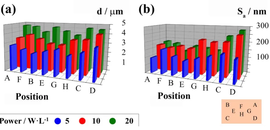
widths of the exposed copper on the anode tool were measured at different locations (A-G) and typically ranged between 200 µm and 240 µm.
Some representative examples of linear features deposited on the A7-sized cathode at 20 mA cm-2 for 720 seconds are shown in Figure 6a. The figure shows relatively well-defined lines with widths of 230 - 290 µm. This can be compared to the anode tool line-widths of 200 - 240 µm which indicates that current spread is limited to 15% and does not appear to increase with the current density. This is a large improvement on earlier experiments at higher US powers using the same linear patterned anode tool which typically resulted in 250% current spreading [24]. In addition, the pattern is transferred over the entire area of the A7 substrate with good definition. This demonstrates the feasibility of transferring patterns using this technique on to large substrates at low US powers.
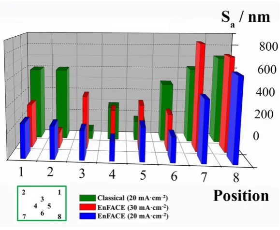
In order to further assess the performance of the method, a thickness and roughness analysis was also performed. The thickness data is presented in Figures 7, 8 and Table 3 and also in Figures 5S, 6S and 7S. The average thickness of the lines was measured over two lines that that corresponded to the locations of the centimetre-scale square features. The thickness data summarised in Figure 8 indicates excellent uniformity over the entire substrate at both current densities. The average surface roughness amplitude (Sa) in Figures 9, 10 and 8S is marginally lower in the centre than at the edges, and increases with current density. In the latter case, this may be due to the limiting current being approached with a corresponding increase in roughness. The low values for the current efficiencies in
Table 3 are more difficult to interpret. Possibly they arise because the limiting current has been exceeded but, interestingly, the through-mask data performed under similar mass transport conditions has a much higher current efficiency.
14
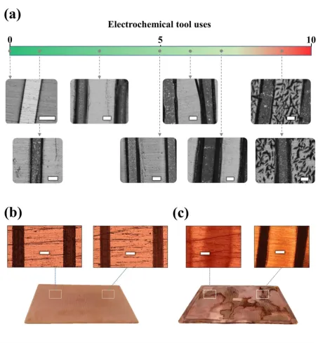
optical micrographs. The gradual degradation of the resist pattern on the anode tool is clearly visible with repeated use (Figure 11a). The damage begins to become clearer after five uses, where the isotropically etched copper has significantly undercut the resist pattern (black lines). After six to seven uses the resist begins to delaminate and undercutting continues. After the ninth experiment, the
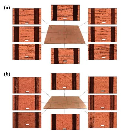
tool becomes unusable due to resist lamination.
Figures 11b and 11c show the optical micrographs and profiles of the copper lines transferred to the cathode for the first and seventh use, respectively. The results in Figure 11 indicate that it is possible to re-use the tool at least five times in the presence of low US power. In the earlier study [24] performed at higher US powers with the same linear pattern dimensions, delamination of the resist were observed after a single experiment. Although the tool life is limited, this still represents an 80% reduction in the amount of lithography processing required compared to conventional through-mask plating. In comparison, earlier experiments employing smaller substrate sizes (1 cm) and positive and negative-tone liquid photoresists typically allowed ten pattern transfers to be obtained from a single tool [20]. Clearly, ultrasonic power has the potential to damage the dry-film photoresist but the previous results indicate that the use of liquid photoresists with improved adhesion could further increase the life-time of the tool. These are difficult to apply to large area rectangular substrate using conventional spin-coating techniques, but spray coating is also feasible [35].
15
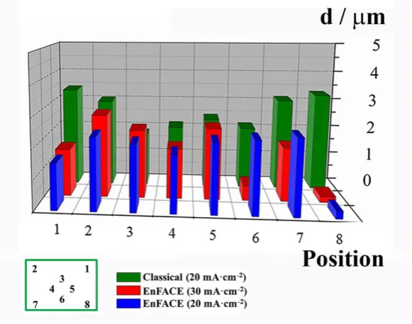
Table 2. Notably, the deposit uniformity obtained for the classical through-mask methodology is poorer than the maskless method, and there is a pronounced edge to centre thickness variation.
The main limitation of the proposed technique is the current spreading effect. This is largely unavoidable, and is mainly controlled by the electrode gap, resistivity of the electrolyte and flatness of the substrate [20, 37]. In the current work, large features (10 x 10 mm2 squares) showed an increase in feature size of around 10% compared to the tool features. For the linear pattern (210 μm x 78 mm) there is an increase of 15% in width. In previous studies [20] using smaller substrates without US agitation, current spreading was typically greater than 20% for 100 – 200 μm wide lines. This increase in feature size is generally not an issue as long as it is reproducible. Under these conditions, it is always possible to reduce the tool feature size to compensate for the current spreading effect, and such mask biasing is often used in conventional microfabrication [35]. Such strategies should enable the maskless technology to be a viable microfabrication process for large substrates. In all other aspects such as thickness, roughness and uniformity the process is comparable to conventional though mask plating.
CONCLUSIONS
Copper pattern transfer experiments of centimetre squares and micrometre lines have been performed in a 18 L ultrasonic tank on to large area substrates (A7 sized copper plates) using the EnFACE technology. The purpose of these experiments was to test the scalability of this mask-less electrochemical patterning method, as previous experiments had been performed on relatively small substrates. A secondary aim was to determine if the process would work at relatively low US powers as earlier experiments had shown a number of issues at higher powers. The final objective was to determine if the additives typically used in copper plating would still function effectively in an acid-free bath with an unconventional agitation scheme.
16
current data can be obtained. The results of this study indicated that, even at a relatively low US power of 5 W L-1, limiting current densities of 40 – 45 mA cm-2 are obtainable. Limiting current at the centre and edges were similar which indicates that mass transport is relatively constant across the substrate. The observed limiting currents are sufficient to allow copper plating at a rate of 20 mA cm-2
which is comparable to current industry practice.
Pattern transfer at the centimetre scale using the maskless process was performed at various US powers with a fixed current density of 20 mA cm-2. The degree of current spreading was found to increase with applied US power and the current efficiency was also lower at the highest powers. The dependence of the deposit roughness on ultrasonic power was harder to ascertain but there was a general tendency for it to be lowest at the highest powers. Collectively, these results indicated that good pattern definition could be achieved at a US power of 5 W L-1 which is much lower than had been used previously [24, 36]. All subsequent experiments were performed under these optimum conditions.
Pattern transfer at the micrometre scale using the process was then demonstrated at 5 W L-1 and at current densities of 20 mA cm-2 and 30 mA cm-2. The degree of current spreading was about 15% which is comparable to that for the centimetre scale experiments (10%) under the same conditions. Increasing the current density to 30 mA cm-2 did not increase the degree of current spreading but it did reduce the current efficiency and increase the surface roughness. Therefore, the optimum conductions for the micrometre pattern transfer were 5 W L-1 and 20 mA cm-2. A comparison was also made against the conventional through-mask plating technique, under the same deposition conditions. As expected through mask plating resulted in 0% current spreading, although the surface roughness was slightly higher than for the maskless one and the thickness uniformity worse. The current efficiency was, however, higher and close to the theoretical value for copper deposition below the limiting current.
17
significant saving in resist processing compared to conventional through-mask plating. With additional improvements in resist technology it is likely that the tool life can be extended further. Collectively, these findings indicate that the technology is a promising electrochemical microfabrication process for large-scale substrates.
Acknowledgements
This work was supported by EU ‘MESMOPROC’ Grant 303550. The Mechanical Workshop of
18
References
[1] P.C. Andricacos, C. Uzoh, J.O. Dukovic, J. Horkans, H. Deligianni, Damascene copper electroplating for chip interconnections, IBM J. Res Dev., 42 (1998) 567.
[2] K. Kondo, R.N. Akolkar, D.P. Barkey, M. Yokoi (Eds), Copper Electrodeposition for Nanofabrication of Electronics Devices, Springer, 2014.
[3] M. Datta, T.Osaka, J.W. Schultze (Eds) Microelectronic Packaging, CRC Press, Boca Raton, 2005.
[4] M. Datta, D. Landolt, Fundamental aspects and applications of electrochemical microfabrication, Electrochim. Acta, 45 (2000) 2535.
[5] J. Rickerby, J. H. G. Steinke, Current trends in patterning with copper, Chem. Rev., 102 (2002) 1525.
[6] L.T. Romankiw, E.J.M. O’Sullivan in Handbook of Microlithography, Micromachining and Microfabrication, Vol. 2 (Editor: P. Rai-Choudhury), SPIE Optical Engineering Press, Bellingham, 1997.
[7] E.J.J. Kruglick, A.L. Cohen, C.A. Bang in The MEMS Handbook, 2nd Edition (Editor: M. Gad-el-Hak), CRC Press, Boca Raton, 2006.
[8] P. Möller, M. Fredenberg, M. Dainese, C. Aronsson, P. Leisner, M. Östling, Metal Printing of copper interconnects down to 500 nm using ECPR – Electrochemical pattern replication, Microelectron. Eng., 83 (2006) 1410.
[9] J.D. Madden, I.W. Hunter, Three-dimensional microfabrication by localized electrochemical deposition, J. Microelectromech. Sys., 5 (1996) 24.
[10] J.D. Whitaker, J.B. Nelson, D.T. Schwartz, Electrochemical printing: software reconfigurable electrochemical microfabrication, J. Micromech. Microeng., 15 (2005) 1498.
19
[12] D. Xu, X. Shi, G. Guo, L. Gui, Y. Tang, Electrochemical preparation of CdSn nanowire arrays, J. Phys. Chem. B, 104 (2000) 5061.
[13] A. Serrà, E. Gómez, J. F López-Barbera, J. Nogués, E. Vallés, Green electrochemical template synthesis of CoPt nanoparticles with tunable size, composition, and magnetism from microemulsions using an Ionic Liquid (bmimPF6), ACS Nano, 8 (2014) 4630.
[14] A. Serrà, E. Gómez, E. Vallés, Novel electrodeposition media to synthesize CoNi-Pt core@shell stable mesoporous nanorods with very high active surface for methanol electro-oxidation, Electrochim. Acta, 174 (2015) 630.
[15] C. Li, T. Sato,Y. Yamauchi, Electrochemical synthesis of one-dimensional mesoporous Pt nanorods using the assembly of surfactant micelles in confined space, Angew. Chem. Int. Ed., 125 (2013) 8208.
[16] J. B. Nelson, D. T. Schwartz, Electrochemical factors controlling the patterning of metals on SAM-coated substrates, Langmuir, 23 (2007) 9661.
[17] S. Roy, Fabrication of micro- and nano-structured materials using mask-less processes, J. Phys. D Appl. Phys., 40 (2007) 413.
[18] S. Roy, EnFACE: A maskless process for circuit fabrication, Circuit World, 35 (2009) 8.
[19] I. Schönenberger, S. Roy, Micro-scale pattern transfer without photolithography of substrates, Electrochim. Acta, 51 (2005) 809.
[20] Q.-B. Wu, T.A. Green, S. Roy, Electrodeposition of microstructures using patterned anode, Electrochem. Commun., 13 (2011) 1229.
[21] T. Widayatno, “Micropattern Transfer Without Photolithography of Substrate: Ni Electrodeposition using Enface Technology”, PhD Thesis, Newcastle University, July 2013.
20
[23] S.J. Coleman, S. Roy, Electrodeposition of copper patterns using EnFACE technique under ultrasonic agitation, J. Appl. Electrochem., 45 (2015) 889.
[24] S. Coleman, “Scale-up of EnFACE Electrochemical Reactor Systems”, PhD Thesis, Newcastle University, June 2015.
[25] E.M. Dela Pena, N. Bains, A. Hussain, A. Cobley, S. Roy, Effect of additive concentration during copper deposition using EnFACE electrolyte, Trans. IMF, 93 (2015) 288.
[26] T. Kikuchi, T. Uchida, Ultrasonic power measurement by calorimetric method using water as heating material, IEEE International Ultrasonic Symposium, 6724830 (2013) 1657.
[26] T. Kikuchi, T. Uchida, Calorimetric method for measuring high ultrasonic power using water as heating material, J. Phys. Conf. Ser., 279 (2011) 012012.
[28] Y. Kado, M. Atobe, T. Nonaka, Ultrasonic effects on electroorganic processes. XVIII. A limiting current study on indirect electrooxidation of n-Butylamine with triarylamine redox mediator, Electrochem., 68 (2000) 262.
[29] F. Marken, D. L. Goldfarb, R. G. Compton, Sonoelectrochemisrty in highly resistive media – mass – transport effects, Electroanalysis, 10 (1998) 562.
[30] B.G. Pollet, Power Ultrasound in Electrochemistry, John Wiley & Sons, 2012.
[31] S. Coleman, S. Roy, Effect of ultrasound on mass transfer during electrodeposition for electrodes separated by a narrow gap, Chem. Eng. Sci., 133 (2014) 35.
[32] J. P. Lorimer, B. Pollet, S. S. Phull, T. J. Mason, D. J. Walton, Disc and cylindrical electrode with ultrasound, Electrochim. Acta, 43 (1998) 449.
[33] D. Pletcher, F.C. Walsh, Industrial Electrochemistry, 2nd Edition, Blackie Academic & Professional, 1993.
21
[35] S. Franssila, Introduction to Microfabrication, 2nd Edition, John Wiley & Sons , 2010.
22
Tables:
Power / W L-1
Limiting Current / mA cm-2
Diffusion Layer, δ / µm
B F B F
5 40 45 34 30
10 50 50 27 27
30 70 70 20 20
Table 1: Limiting current and diffusion layer thickness, δ, at different ultrasonic powers. Values are
23
US Power
W L-1
Af / cm2 Lf /
cm
Average Thickness (d) / µm
Average Roughness (Sa) /
nm ε / %
Corners Middle All
Areas Corners Middle
All Areas 5
8.6 ± 0.2 1.0 4.6 4.2 4.4 220 140 180 96
10
9.7 ± 0.4 1.1 3.8 3.2 3.5 200 190 195 87
30 12.7 ± 0.2 1.3 2.8 2.4 2.6 140 120 130 85
24
Current density / mA cm-2
Line widths /
µm
Average Thickness (d) / µm Average Roughness (Sa) / nm
ε / %
Corners Middle All
Areas Corners Middle
All Areas
EnFACE methodology
20 260 ± 30 2.1 2.3 2.2 420 214 315 60%
30 255 ± 25 1.8 2.3 2.0 521 355 438 55%
Though-mask plating methodology
20 220 ± 15 3.2 2.4 2.8 630 249 440 87%
25
26
[image:26.595.122.475.203.472.2]27
[image:27.595.149.462.230.463.2]28
[image:28.595.182.414.196.566.2]29
[image:29.595.171.427.223.424.2]30
[image:30.595.79.522.223.437.2]31
32
33
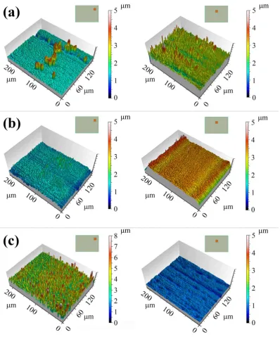
[image:33.595.154.445.281.510.2]Figure 7: 3D thickness profilesof linear copper patterns at: (a) 20 mA cm-2 and (b) 30 mA cm-2 using the maskless method and (c) at 20 mA cm-2 using through-mask plating. All experiments were performed at a US power of 5 W L-1.
34
[image:34.595.101.500.76.556.2]35
[image:35.595.154.444.228.466.2]36
37
SUPPORTING INFORMATION:
Sono-electrodeposition transfer of micro-scale copper
patterns on to A7 substrates using a mask-less method
Albert Serrà a,*, Simon J. Coleman b, Elvira Gómez a, T.A. Green c, Elisa Vallés a, Joan Vilana a, Sudipta Roy c
a Grup d’Electrodeposició de Capes Primes i Nanoestructures (GE-CPN), Departament de
Química Física and Institut de Nanociència i Nanotecnologia (IN2UB), Universitat de
Barcelona, Martí i Franquès 1, E-08028, Barcelona, Spain.
b
School of Chemical Engineering and Advanced Materials (CEAM), Merz Court, Newcastle
University, Newcastle upon Tyne, NE2 7RU, UK.
c
Department of Chemical and Process Engineering, University of Strathclyde, James Weir
Building, 75 Montrose Street, Glasgow, G1 1XJ, UK.
38
[image:38.595.108.504.222.472.2]39
[image:39.595.101.506.83.638.2]40
Figure 3S: (a) Scheme of the anodic holder with the photolithographed tool (left) and inter-electrode gap separation (right) for pattern electrodeposition with square; (b) Image of the photoresist tool; (c)
[image:40.595.87.512.70.645.2]41
42
43
44
[image:44.595.78.517.71.677.2]45