Generation, Performance Evaluation and Control Design of Single-phase Buck-boost Differential-mode Current Source
Inverters
Journal: IET Renewable Power Generation Manuscript ID: RPG-2015-0343
Manuscript Type: Research Paper Date Submitted by the Author: 23-Jul-2015
Complete List of Authors: Darwish, Ahmed; University of Strathclyde, EEE
Holliday, Derrick; University of Strathclyde, Electronic and Electrical Engineering
Williams, Barry; UNiversity of Strathclyde, Electrical and electronic engineering
Keyword:
DC-AC POWER CONVERTORS, SWITCHED MODE POWER SUPPLIES, PHOTOVOLTAIC POWER SYSTEMS, RENEWABLE ENERGY SOURCES, POWER ELECTRONICS, VARIABLE STRUCTURE SYSTEMS
Generation, Performance Evaluation and Control Design of
Single-phase Buck-boost Differential-mode Current Source Inverters
Ahmed Darwish1*, Derrick Holliday1, Barry Williams1 1
Electrical and Electronic Engineering, University of Strathclyde, Glasgow, UK *
Abstract: Differential-mode inverter topologies are promising for renewable energy generation as they offer merits such as reduced size of passive elements, high power density, and reduced total cost. Single-phase buck-boost differential-mode current source inverters (DMCSI) can provide flexible output voltage above or below the input dc voltage, which is necessary for higher efficiency of modern renewable energy applications. The continuous input current of a DMCSI is appropriate for maximum power point tracking operation (MPPT) of photovoltaic applications. However, the performance and control of such converters has not been discussed in detail. As a drawback, the total dc side input current of a single-phase inverter consists of a desired dc component and an undesirable ac component. This ac current component frequency is double the output voltage frequency and thus, affects MPPT resulting in reduced total efficiency. In this paper, five possible DMCSIs are proposed and compared in terms of total losses, maximum ripple current, total harmonic distortion, devices and passive element ratings. In addition, the sliding mode controller’s design and possible methods of eliminating the input 2nd harmonic current are discussed. A 2.5kW bidirectional inverter is used to validate the design flexibility of the five inverters topologies.
1. Introduction
There is mounting international proclivity to reduce the cost and improve the efficiency of energy conversion systems through modular structured renewable/distributed systems [1]. Therefore, the need for reducing converter size and passive component values is pressing. Moreover, the cost of photovoltaic (PV) systems is affected considerably by installation and maintenance costs [2]. The inverter initial and running costs may reach about half the initial PV system cost [3].
Most dc-ac converters installed in PV systems require large input filtering capacitance, typically wet electrolytic types. Replacing this electrolytic capacitor with a plastic type increases reliability significantly as it is at least thirty times more reliable than electrolytic types, at the same operating conditions [4]. At rated operating conditions, the life time of an electrolytic filter capacitor is short compared with other inverter components [5]. Thus, using this capacitor hampers increased overall system reliability. The life time of a capacitor is halved for every 10oC increase in the operating temperature [6].
10]. Myrzik [11] classified the single-stage buck and boost inverter topologies, while in [12], buck-boost Z-source inverter topologies were proposed and explained.
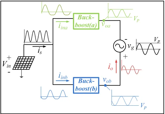
If two power converters are connected in a parallel-series configuration, they form a differential-mode inverter. Some of these differential mode inverters types are shown in [9], [13, 14]. The basic structure of a differential-mode buck-boost single-phase inverter is shown in Fig.1. The differential-mode inverter initially appeared in [13] as a boost inverter, while a differential buck inverter is presented in [15]. Knight et al. [2] proposed the differential six-switch buck-boost inverter based on the Ćuk converter, but its performance was not evaluated.
Of the known two-switch two-diode buck-boost reversible converters, there are five converters that can provide continuous input currents and hence, mitigate the need for large electrolytic input capacitors. These buck-boost converters are shown in [16] as C5, D1, D2, F5 and G5 and can be used as building blocks in a differential-mode current source inverter (DMCSI). Besides eliminating an unreliable large electrolytic capacitor, continuous input current switched mode power supplies (SMPS) enable safe and reliable converter-grid connection and they are attractive solutions for energy conversion systems in terms of: 1) voltage buck-boost operation with a flexible output voltage range, 2) continuous input current, 3) high efficiency, and 4) high frequency transformer coupling possibilities.
Generally, continuous input current converters are time variant systems where the overall transfer function describing the relation between the input and output voltages and currents depend on the switching periods of its switches. This results in a complex stable design because the converter poles and zeros travel through a long Nyquist trajectory [9], [17, 18].
component which requires another stage of filtering. An active harmonic suppression technique is presented in [23], where the 2nd order harmonic of the input current is eliminated by a series buffer converter topology.
[image:4.612.124.411.225.423.2]This paper presents the generation of single-phase buck-boost DMCSIs from their building dc-dc blocks, proposes proper control design for each topology, and compares the possible DMCSI topologies in terms of features such as efficiency, input current ripple, output current total harmonic distortion (THD), and device and capacitor ratings. Also the paper presents possible methods for decoupling the 2nd order harmonic current components in the proposed DMCSIs with and without extra power electronic switches and discusses their effect on passive element sizes.
Fig.1. Basic structure of a buck-boost DMCSI.
2. System description
The input voltage dc source is connected to two bidirectional buck-boost converters as shown in Fig.1. Most buck-boost converters produce an output voltage which has an opposite polarity to the input voltage. Each converter produces unipolar voltage where:
( )
oa t h Va in
v = −
sin
a Hdc Hac t
h = + ω
( )
½
[1 sin
]
oa
t
V
t
v
= −
p
+
ω
(1a)
( )
ob b in
v t = −h V⋅
( ) sin( )
b t Hdc Hac t
h = +
ω
−π
½
( )
p[1 sin(
)]
ob
t
V
t
v
= −
+
ω π
−
(1b)
( ) sin
( ) sin( )
ω ω γ
= − =
= +
g ob oa p
o o
t V t
v v v
t I t
i
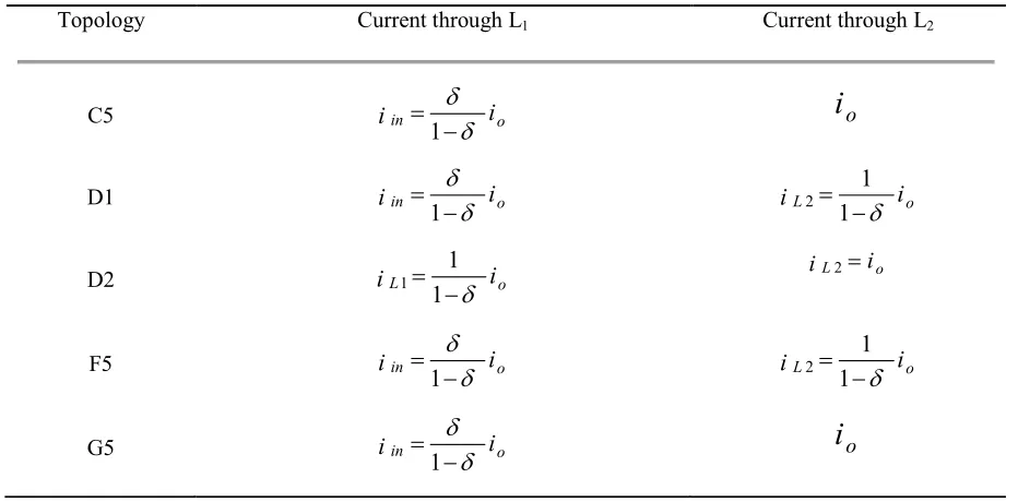
( 1c) The basic dc-dc converters with continuous input currents are shown in Fig. 2. All are reversible when using two switch-diode pairs. For all these converters, the power is transferred from the input to the output side (or in the opposite direction) through a capacitor C while storing energy in the input and output inductors L1and L2. For converters C5, D1 and D2, the output shunt capacitor Co is optional (converters the
output to a voltage source) as the output current is continuous. However, Co is mandatory for converters
G5 and F5 (in order to average the output voltage). For all the converters, the switch and diode (S1 and D2)
operate alternately when the power is transferred from the input to the output and the switch and diode (S2
and D1) operate alternately when power is transferred in the opposite direction. ton is the period when S1 or
D1 conduct current while toff is the period where S2 or D2 conduct.
c
a d
b e
Fig. 2. Buck-boost converters with continous input current: (a) C5 (Ćuk), (b) D1, (c) D2, (d) F5, and (e) G5 (sepic).
The switch on-state duty ratio of the converters δ is: on
s
t
t
=
δ
(2a)r
1,L
1r
2,L
2v
c+
-V
inS
1D
1S
2D
2i
in+
-C
ov
oC/2
i
L2The voltage conversion ratio between the output and input voltages (h) can be expressed as: 1 δ δ = = = − in o o in v i h
V i (2b)
The five buck-boost converters can be inserted into the configuration blocks in Fig.1. The time varying duty ratios of the converters can be deduced from the desired output voltages as:
( ) a and ( ) b
a b
a b
h h
t t
h 1 h 1
δ
=δ
=+ + (3)
3. Converter performance comparison
In this section, the five single-phase buck-boost DMCSIs are discussed and compared in terms of: 1) overall efficiency, 2) input current ripple, 3) switch and diode currents and voltages, 4) output current THD, and 5) capacitors voltage stresses. To avoid duplication and prolongation, the mathematical analysis for only the C5 (Ćuk) converter will be presented in detail while the final conclusions for the remaining four converters will be summarised.
3.1. Power Losses
Two significant loss sources will be considered in this analysis. The first is the copper (I2R) loss in the input and output inductors and the second is converter semiconductor device losses. Consequently, the root mean square (rms) currents in the inductors as well as the average current in the diodes should be derived. The currents through inductors L1 and L2 can be expressed as functions of the output current,
[image:6.612.74.540.443.673.2]voltage and duty ratios as shown in Table 1.
Table 1 Currents through the converter’s inductors
Topology Current through L1 Current through L2
C5
1
in io
i δ
δ
=
−
i
oD1
1
in io
i δ δ = − 2 1 1
L io
i
δ
= −
D2 1
1 1
L io
i
δ
= −
2 L io i =
F5
1
in io
i δ δ = − 2 1 1
L io
i δ = − G5 1
in io
i δ
δ
=
1 1−δ
is always greater than 1 while 1
δ δ
− is greater than 1 when δ> 0.5 and less than 1 when δ< 0.5. For C5 converters, as an example, the instantaneous input current iina and iinb of each converter is:
( )
,
( )
1
δ
δ
=
=
−
ina oa a
o in a
t
v
i
t
V
i
( )
( )
1
δ
δ
=
=
−
inb ob b
o in b
t
v
i
t
V
i
(4a)( ) ½[ sin ] sin( )
{½ cos ½ cos(2 ) sin( )}
2
ω
ω
γ
γ
ω
γ
ω
γ
= + + = + + + + p p ina o in in p o in V V
t t I t
i V V I V t t V (4b)
( ) ½[ sin( )] sin( )
{½ cos ½ cos(2 ) sin( )}
2
ω
π
ω
π γ
γ
ω
γ
ω
γ π
= + + + + = + + + + + p p inb o in in p o in V V
t t I t
i V V I V t t V (4c)
The inputs current iina and iinb are rewritten as:
1 2
1 2
1
2
( ) sin( t ) cos(2 t )
( ) sin( t ) cos(2 t )
¼ cos
½
¼
ω γ ω γ ω γ π ω γ
γ = + + + + = + + + + + = = =
ina in in in
inb in in in
o p in in o p in in o p in in t
i I I I
t
i I I I
V I I V V I I V V I I V (5)
If the parasitic resistances of the inductors (L1and L2) are assumed as r1 and r2, the copper losses are:
2 2
2
1 2 1 _
2 2 _
(
½
½
)
½
=
+
+
=
in in in loss inloss out o
P
I
I
I
r
P
I r
(6)
The power losses through the switches can be approximated as: 2
2 2 2
1
1 2
where
3 3 1.3
( ),
2 4 16 1
½ ,
δ
δ
π
π
= + ≈ + ≈ + + = − = Dsw DF on rms
av o dc ac dc
rms av
dc ac
in o
D in D
P V i R I
I H H H
I
H H
I I
i I i
(7)
The total power loss of each inverter is:
_ _
2[ ]
= + +
total loss in loss out sw
P P P P (8)
and the inverter efficiency is:
100
η = ×
+ p o
p o total V I
V I P (9)
The switches power losses in the five inverter types are the same as they all have identical current and voltage waveforms. The copper losses as well as device average voltage and current are summarized in Table 2.
Table 2 Copper losses and switch operating conditions Type
Copper losses x r Switch averages
L1 L2
S1 and D1 S2 and D2
Voltage Current Voltage Current
C5 3
16
2 2 −
8 2
G5 3
16
2 '' '' '' ''
D1 3
16
8 + (2 + 1) '' '' '' ''
D2
8 + (2 + 1)
2 '' '' '' ''
F5 3
16
[image:8.612.153.455.413.607.2]
2 '' '' '' ''
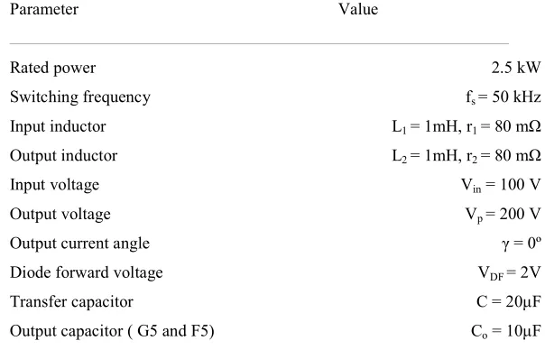
Table 3 Parasitic component values and circuit conditions
Parameter Value
Rated power 2.5 kW
Switching frequency fs = 50 kHz
Input inductor L1 = 1mH, r1 = 80 mΩ
Output inductor L2 = 1mH, r2 = 80 mΩ
Input voltage Vin = 100 V
Output voltage Vp = 200 V
Output current angle γ = 0º
Diode forward voltage VDF = 2V
Transfer capacitor C = 20µF
Output capacitor ( G5 and F5) Co = 10µF
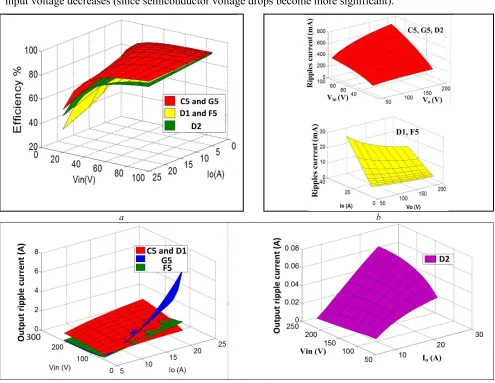
better than both when the input voltage is low. Generally, the efficiency of all inverters decreases as the input voltage decreases (since semiconductor voltage drops become more significant).
a b
c
Fig. 3. MATLAB simulation of DMCSIs: (a) efficiency, (b) input current ripple ∆Iin, and (c) output current ripple ∆Io
3.2 Input current ripple
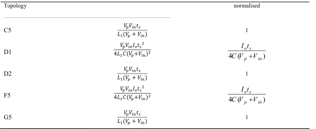
[image:9.612.59.554.76.459.2]same input current ripple versus output current and voltage. As an important advantage, the ripple contents of the input current iin in D1 and F5 are small compared with the other DMCSIs.
Table 4 Maximum Input current ripple
Topology normalised
C5
(+ ) 1
D1
4(+ ) 4 ( + )
o s
p in
I t
C V V
D2
(+ ) 1
F5
4(+ ) 4 ( + )
o s
p in
I t
C V V
G5
(+ ) 1
3.3 Output current ripple
The output current distortion can be classified into low frequency and high frequency distortion. Low order current distortion appears because of the non-linear nature and high system order of the proposed inverters and can be removed with appropriate control loops as discussed in [9]. The high frequency current and voltage ripple in the output side is because of the switching action. These high frequency ripple components are dependent on the converter topology the differential-inverter descends from. For the same passive element component values, the output current ripple can be expressed as in Table 5. The peak output current ripple ∆Io of the different inverters are simulated in Fig. 3c. The high frequency ripple
component of the output current Io in D2 is insignificant compared with the other converters, with the
Table 5 Output current ripple
Topology normalised
C5
(+ )
1
D1
(+ )
1
D2
4(+ ) 4 ( + )
o s
p in
I t
C V V
F5
(+ )
2 4
o o in
I C V
L
G5
(+ )
2
4 ( + )
o o Vp in
L I
C V
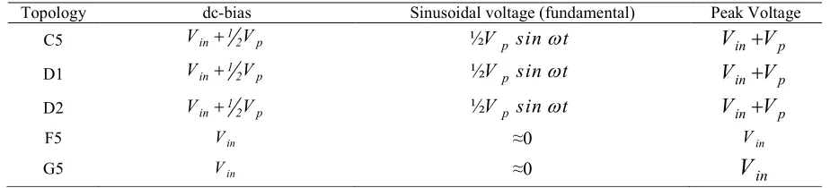
3.4 Capacitor C voltage stress
[image:11.612.73.535.431.536.2]Knowledge of the voltage stresses on the energy transfer capacitor C is important for its selection. For some inverters, the voltage across C consists of a dc-bias plus a sinusoidal voltage component (fundamental) while for other converters, the voltage across C is only dc. Inverters using F5 and G5 have lower capacitor voltages stresses than C5, D1 and D2. Table 6 summarize the capacitor voltages stresses for each converter, in terms of the source voltage and differential sinusoidal output maximum voltage, Vp.
Table 6 Voltage stress across capacitor C (see Fig. 1)
Topology dc-bias Sinusoidal voltage (fundamental) Peak Voltage
C5 Vin+12Vp ½V p sin ωt Vin+Vp
D1 Vin+12Vp ½V p sinωt Vin+Vp
D2 Vin+12Vp ½V p sinωt Vin+Vp
F5 Vin ≈0 Vin
G5 Vin ≈0
V
in4. Control design
analysis will be presented in detail for the C5 based system and following the same approach, the final block diagrams and control equations will be stated for the other four inverter types. SMC forces the system states to track predefined trajectories which lie on the desired reference values [25]. SMC having fast dynamics and its robustness to system parameter and states variations are important features. The control structure aims to drive the inverter’s output current io on a specified surface. First, the large signal
average model of C5 converter can be obtained from the converter’s differential equations in the on and off modes as follows (continuous conduction mode (CCM) of all passive reactive components is ensured because the converters are reversible):
i) S1 OFF and S2 ON (0 < t <toff)
in 1
in o c
1 1 1
di 1 r 1
= V - i - v
dt L L L
(10)
c in
dv 1
= i
dt C
o 2
o o
2 2
di r 1
= - i - v
dt L L
ii) S1 ON and S2 OFF (toff< t <ts)
in 1
in in
1 1
di 1 r
= V - i
dt L L
(11) c
o
dv 1
= i
dt C
o 2
c o o
2 2 2
di 1 r 1
= - v - i - v
dt L L L
The equations can be averaged over the switching time ts as:
in 1
in in c
1 1 1
di 1 r 1 - u
= V - i v
dt L L − L
(12)
c
in o
dv u 1 - u
= i i
dt C +C
o 2
c o o
2 2 2
di u r 1
= - v - i - v
dt L L L
{ 1
1
1 S on
0 S off
u =
By averaging the discrete variable u on ts as ueq = δ, the average state space model in the continuous
2
0
0 0 0
0 0
in 1
in
1 1 1
in c c o o 2 o 2 2
di r (1 - ) 1
- - i 0
dt L L L
V
dv (1 - )
v
dt C C
v
di r 1
- i
dt L L L
δ δ δ δ = + − (13)
The C5 converter is not able to be controlled directly from the output current; only the input current can be directly controlled. This can be understood from the effect of the two switches S1 and S2 on the converters
currents. For all the converters in Fig. 2, S1 affects the input current iin directly while S2 has no direct effect
on io. For this reason, the reference value of the converter output current is written in terms of iin. The
sliding surface ‘S’ can be chosen as:
= + + (14a)
= + + = 0 (14b)
where α1, α2 and α3 are constants and e1, e2and e3 are the controller error signals, written as: = ∗ −
= ∗−
= "(+ )#
(15a) = # ∗ # −# # = # ∗ # −# # = + (15b)
For the pre-stated controllability issues, the reference input current i*in is re-written as:
∗ = $(
∗− ) (16)
where K is a control constant. If the frequency of i*o is assumed small compared to the switching
frequency, i*o can be considered constant during one switching period and its derivative can be considered
as zero. Substituting (13) and (16) into (15a) yields:
δ δ
+ 1 + + 2 +
1 in in c o o
1 1 2 1 2 2
r K r
-1 K (1 - ) K
e = V i v (- + ) i v
L L L L L L
&
(17)
δ + 2 +
2 c o o
2 2 2
r 1
e = - v i v
L L L
&
* o
3 o in
e = (K +1)(& i - i ) - i
Substituting (17) into (14a) and solving for δ gives:
* in in 1 1 c o 2 2 o 2 3 o o eq
c 2
-V i ( r K ) v i ( K r ) v K K ( i i )
u =
v ( 1 K )
δ + − + + + + −
=
+
3 1 2 3
1 1 2 1 3 1
1 2 1 1
1 and ( K )
K
K L , K L , K L
L
α α α α
α α α
+ +
= = =
The resultant sliding mode controller from (18) is shown in Error! Reference source not found.a.
The controller gains K1, K2 and K3 are responsible for steady state regulation, oscillation and settling time.
The designer has three degrees of freedom to choose the gain values. However, it must be confirmed that these values ensure tracking of the predefined trajectory. This is confirmed by fulfilling two existence conditions [26]:
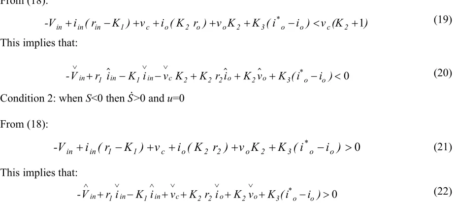
Condition 1(Lyapunov): when S>0 then <0 and u=1 From (18):
1
*
in in in 1 c o 2 o o 2 3 o o c 2
-V +i ( r −K ) v+ +i ( K r ) v K+ +K ( i −i ) <v (K + ) (19)
This implies that:
0
*
in 1 in 1 in c 2 2 2 o 2 o 3 o o
-V r i K i v K K r i K v K ( i i )
∨ ∨ ∨
+ $ − − + $ + $ + − < (20) Condition 2: when S<0 then >0 and u=0
From (18):
0
+
−
+
+
+
+
*−
>
in in 1 1 c o 2 2 o 2 3 o o
-V
i ( r
K ) v
i ( K r ) v K
K ( i
i )
(21)This implies that:
0
*
in 1 in 1 in c 2 2 o 2 o 3 o o
-V r i K i v K r i K v K ( i i )
∧ ∨ ∧ ∨ ∨ ∨
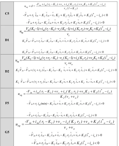
[image:14.612.64.527.187.394.2]+ − + + + + − > (22) Equations (20) and (22) are referred to as existence equations. The sliding mode controllers for the other inverters are similarly obtained. The block diagrams of the other four buck-boost DMCSIs are shown in Fig. 4 while the associated existence equations are listed in Table 7.
5. Experimental results
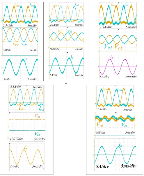
The system concept, presented mathematical analysis, and simulations, are validated with a 2.5kW DMCSI as in Fig.1, with the parameters in Table 3, controlled with TMS320F280335 DSP. Fig. 5 shows the experimental rig, while Fig. 6 shows the experimental results for the presented analysis and discussion for the buck-boost DMCSIs when controlled by sliding mode control and connected to the grid (Vp = 200V)
a b
c d
e
Fig. 4. Block diagrams of DMCSI sliding mode controllers: (a) C5, (b) D1, (c) D2, (d) F5, and (e) G5
Table 7 Control and existence equations
C5
* in in 1 1 c o 2 2 o 2 3 o o eq
c 2
-V i ( r K ) v i ( K r ) v K K ( i i )
u =
v ( 1 K )
δ + − + + + + −
=
+
0
*
in 1 in 1 in c 2 2 2 o 2 o 3 o o
-V r i K i v K K r i K v K ( i i )
∨ ∨ ∨
+ $ − − + $ + $ + − <
0
*
in 1 in 1 in c 2 2 o 2 o 3 o o
-V r i K i v K r i K v K ( i i )
∧ ∨ ∧ ∨ ∨ ∨
+ − + + + + − >
D1
2
1
21
*
in in 1 1 c o 2 2 o 2 3 o o
eq
c
V ( K
) i ( r K ) v ( K
) i ( K r ) v K
K (i
i )
u
v
− +
−
−
− +
+
+
−
=
2 2 2 2 0 0 * in in 1 in 1 in c c 2 2 o 2 o 3 o o* in in 1 in 1 in c 2 2 o 2 o 3 o o
K V V r i K i K v v K r i K v K ( i i )
K V V r i K i K v K r i K v K ( i i )
∨ ∧ ∨ ∧ ∧ ∨ ∨ ∨
∧ ∨ ∧ ∨ ∨ ∧ ∧
− + − − + + + + − >
− + − − + + + − <
D2
2
− +
1
+ −
−
2− +
1
+
+
−
=
+
*
in in 1 2 1 c o 2 2 o 2 3 o o
eq
c o
V ( K
) i ( r r
K ) v ( K
) i ( K r ) v K
K ( i
i )
u
v
v
2 2
2 2 2
0
0
* in in 1 2 in 1 in c c 2 2 o 2 o 3 o o
* in in 1 2 in 1 in c 2 o 2 o o 3 o o K V V ( r r ) i K i K v v K r i ) K v K ( i i )
K V V ( r r ) i K i K v K r i K v - v K ( i i )
∨ ∧ ∨ ∧ ∧ ∨ ∨ ∨
∧ ∨ ∧ ∨ ∨ ∧ ∧ ∨
− + + − − + + + + − >
− + + − − + + + − <
F5
*
in in 1 1 c o 2 2 o 2 3 o o
eq
2 c o
-V
i ( r
K ) v
i ( K r ) v K
K ( i
i )
u
K ( v
v )
+
−
+
+
+
+
−
=
+
2 0 0 * in 1 in 1 in c 2 2 o 2 o 3 o o* in 1 in 1 in c c 2 2 o 3 o o V r i (min) K i v K r i K v K ( i i )
V r i K i K v - v K r i K ( i i )
∧ ∧ ∨ ∨ ∨
∨ ∧ ∨ ∨ ∧ ∧
− + − + + + + − >
− + − − + + − <
G5
+
−
+
−
+
+
−
=
+
*
in in 1 1 c o 2 2 o 3 o o
eq
c o
-V
i ( r
K ) v
i ( K r ) v
K ( i
i )
u
v
v
0
*
in 1 in 1 in c 2 2 o o 3 o o
V r i K i v K r i v K ( i i )
∧ ∨ ∧ ∨ ∧ ∨
− + − + − + + − >
0
* in 1 in 1 in 2 2 o 3 o o
V
r i
K i
K r i
K ( i
i )
∨ ∧ ∨ ∨
−
+
−
−
+
−
<
D2 has the lowest THD while C5 and D1 have the highest. Both D1 and F5 have the lowest input current ripple. However F5 and G5 require output capacitor Co, while the voltage stresses across the
a b c
d e
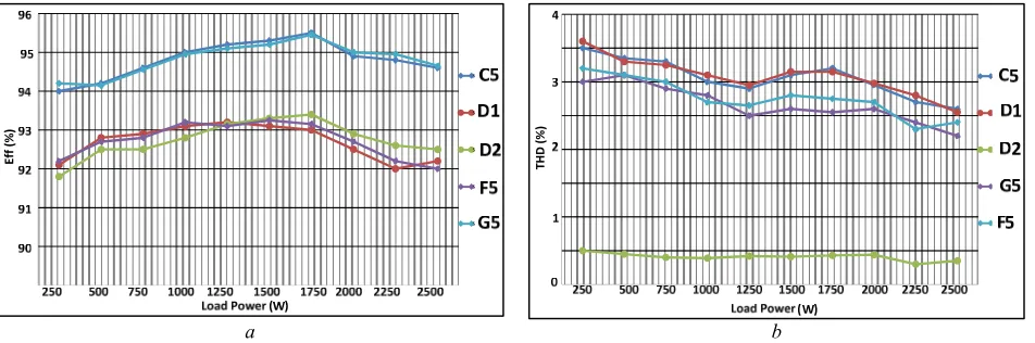
[image:17.612.61.556.44.649.2]a b Fig. 7. Experimental plots of DMCSIs: (a) efficiency and (b) THD.
6. Dc side harmonic filtering
Single-phase inverters draw and deliver oscillating power, with the second-order current harmonic (superimposed on an average dc current) in the dc link (the dc side), independent of the power flow direction. In low power applications, such as small-scale PV systems for micro-grids, filtering is required at the dc side because the harmonic current components will significantly affect PV MPPT. In [21], a two-switch two-diode reversible boost converter can actively eliminate the second order harmonic component from the input of the PV or EV system currents as shown in Fig. 8a and the energy can be stored temporarily in an output capacitor CHC. However, this harmonic compensator (HC) method requires an
additional power electronic converter which adds to the total cost and control complexity.
The instantaneous power equation of the differential buck-boost inverter with an HC can be written as:
( ) ( ) ( )
( ) ( ) ( )
= +
= +
in HC o
in s HC in g o
P t P t P t
V I i t V v t i t
½ o o
s
in V I I
V
=
( ) ( )
( )= − g o
HC s
in
v t i t
i t I
V
½ cos 2
½
= ω
=
p o HC
in
p o peak
HC
in V I
i t
V V I I
V
(23) Series1
Series2
Series3
Series4
Series5
E
ff
(
%
)
Chart Title
Series1
Series2
Series3
Series4
Series5
T
H
D
(
%
[image:18.612.66.542.75.233.2]a b
c d
Fig. 8. 2nd harmonic elimination of DMCSI: (a) active elimination with additional power electronic converter [21], (b) active elimination without additional power electronic converter, (c) control for the proposed method, and (d) experimental results for C5 DMCSI with the proposed method.
is
iina
iinb
io
vg +
-+
-Vin
Buck-boost(a)
Buck-boost(b)
Harmonic Compensator
LHC
CHC
iHC
iL
VHC (f)
Vi (f)
+
- i
s
iina
vg +
-+
-Vin
va
Buck-boost(a)
Buck-boost(b)
vb
io
iinb
+
-+
-va= +
+
vb=
f=50Hz
f=100Hz
f=50Hz
f=100Hz
ia
ib
Co
The energy (PHC dt) flows from the input side and is stored in the output capacitor CHC in the +ve half
cycle of iHC and vHC(t) increases from VHC(i) to VHC(f). In the -ve half cycle of iHC, the same energy flows
from CHC back to the dc supply leading vHC(t) to decrease from VHC(f) to VHC(i). This energy cycling can
be expressed as:
½
2 2
0
2 2
2
( ) dt ½ [ ( ) ( )] 1
where 2 and ( ) ( )
2 ( )
2
= −
∫
= =
= +
π
= +
π
HC
t
in HC HC HC HC
HC HC in
p o
HC in
HC p o
HC in
HC
V i t C v f v i
t f v i V
V I
v f V
f C
V I
v f v
f C
(24)
The proposed single-phase buck-boost DMCSIs have the capability to decouple the 2nd order harmonic current component without additional power electronic devices. From Fig. 8b, an additional controller forces energy oscillating at 100/120 Hz to be stored instantaneously in the output capacitors Co (which are
necessary for F5 and G5 inverters and optional for C5, D1 and D2 inverters). The controller must ensure that this stored energy does not affect the output voltages and currents. Therefore, two voltages with the same magnitude, phase-shift and 100/120 Hz frequency are superimposed across the output capacitors. Without decoupling the double-frequency power, the output instantaneous power is:
1 2
( ) cos cos(2 )
where
= γ − ω − γ =
P Q
p o
p t S S t
S V I
123 1442443
(25) where Q is the reactive power absorbed by the load
The converter output voltages, va and vb shown in Fig. 8b, can be expressed as:
2 2
2 2
( ) ½ ½ sin sin(2 )
( ) ½ ½ sin( ) sin(2 )
= + ω + ω + ψ = + ω + π + ω + ψ
a p p
b p p
v t V V t V t
v t V V t V t
(26)
Because they are of same magnitude V2, frequency 2f, and phase shift ψ2, the second order components in
the output voltages va and vb do not affect and are not seen by the load voltage vg and current io. That is,
the second order component is eliminate in the output va – vb.
For the C5 DMCSI example, the total reactive power stored in the inductors (L1 and L2) and capacitors (C
1 2
( ) ( ina inb ) 2 o ( ca cb ) ( a b )
s ina inb o ca cb o a b
di di di dv dv dv dv
Q t L i i L i C v v C v v
dt dt dt dt dt dt dt
= + + + + + + (27)
To eliminate the 2nd order harmonic current supplied from the input dc source, the total stored energy in the inverter should be zero. Equating Q to Qs in equations (25) and (27) and solving for V2 and ψ2 leads to:
2 1 2 2 2 tan
4 co s co s 2 co s
− ω ψ = γ γ = ω ψ d p o p C V S S V C V (28)
where Cd = C+Co
However, eliminating the double frequency oscillating power will generate 4th order oscillating power Q4th :
2
4th 2 2 sin(4 2 )
Q = ωV ω + ψt (29)
The emerging 4th order oscillating power will generate 4th order oscillating current in the input side and needs an additional control loop for elimination. In Fig. 8c, a proportional-resonant (PR) controller is implemented in order to ensure suppression of the 2nd and 4th order harmonics from the input current. As the controller’s fast dynamics are not important, the gain values of the PR controller (Kp and Kr) can be
selected much lower than the main loop values in order to avoid interaction. Fig. 8d shows the performance of this controller with Co = 150µF where it removes 75% of the 2nd order harmonic
component in the input current. Fig. 9a shows the voltage stress across the decoupling capacitors (CHC and
Co) for the two active methods, with and without power electronic devices, at different output current and
capacitor values.
a b
Fig. 9. 2nd harmonic elimination of DMCSI : (a) voltage stress across the decoupling capacitor (Co or CHC) for active elimination methods and (b) differential-mode C5 inverter efficiency with 2nd order harmonic currents active elimination techniques. 0 5 10 15 20 0 0.5 1 1.5
x 10-4
0 500 1000 1500 Io(A) Capacitor
(Co or CHC) (Farad)
S tr es s o n C a p a ci to r (V )
W ithout Power Electronics W ith Power Electronics
1 2 3 4 5 6 7 8 9 10 250 500 750 1000 1250 1500 1750 2000 2250 2500 92
93 94 95
With Power Elect. Converter Without Power Elect.
Converter
[image:21.612.67.552.453.606.2]Using additional power electronics results in lower stress on the capacitor CHC (lower plane in Fig. 9a)
than on Co with the second method (upper plane in Fig. 9a). However, Fig. 9b shows that the efficiency of
the second method is higher, since device power losses of the additional power electronic converter decrease efficiency.
7. Conclusion
The paper investigated single-stage single-phase inverters based on two differentially connected reversible buck-boost converters which have advantages when embedded in renewable energy generation systems. The inverters have a low dc side ripple current, without recourse to electrolytic capacitor filtering. The buck-boost converters have nonlinear high order transfer functions where the dynamics depend on the operation point and the duty ratio, which complicates control design. A 2nd order harmonic dc side input current component disturbs MPPT, hence reduces total efficiency. In this paper, five topologies for DMCSIs were proposed. With their operation, features, and control design using sliding mode control were investigated and verified.
The C5 and G5 based inverters have the lowest power loss, hence the highest efficiencies. However, they experience high input current ripple and may require higher input inductors values. The D1 and F5 converters have good efficiency at higher input dc voltages while the efficiency deteriorates at lower input voltages. The efficiency of the D2 inverter is lower than D1 and F5 at high input voltage but is better at lower input voltages. From the devices rating point of view, the five inverters topologies have the same performance. Using the same passive element values, D2 is found to have the lowest THD in the output voltage and current waveforms. D1 and F5 inverters have low input ripple current which is attractive feature for PV systems. F5 and G5 inverters have the lowest capacitor voltage stresses, hence smaller and cheaper capacitors can be used.
A new active method to suppress the 2nd order harmonic input current from the DMCSIs without additional power electronic converters is proposed. The 2nd order reactive power is decoupled using the inverter output capacitors in the ac side. Comparing the proposed technique with a power electronic based active elimination method, the proposed method avoids the power losses associated with an additional power electronic converter, which reduces system efficiency.
8. References
[1] Thomson, M., Infield, D.G.: 'Impact of widespread photovoltaics generation on distribution systems', Renewable Power Generation, IET , vol.1, no.1, pp.33–40, March 2007
[2] Knight, J., Shirsavar. S., and Holderbaum, W.: 'An improved reliability Ćuk based solar inverter with sliding mode control', IEEE Transactions on Power Electronics, vol. 21, pp. 1107-1115, 2006.
[3] Naik, R., Mohan, N., Rogers, M., and Bulawka, A.: 'A novel grid interface, optimized for utility-scale applications of photovoltaic, wind-electric, and fuel-cell systems', IEEE Transactions on Power Delivery, vol. 10, pp. 1920-1926, 1995.
[4] 'Reliability Prediction for Electronic Equipment',Doc. MIL-HDBK- 217X, Dec. 1991.
[5] Hongbo, M., Jih-Sheng, L., Quanyuan, F., Wensong, Y., Cong, Z., and Z. Zheng: 'A Novel Valley-Fill SEPIC-Derived Power Supply without Electrolytic Capacitor for LED Lighting Application', IEEE Transactions on Power Electronics, vol. 27, pp. 3057-3071, 2012.
[6] Hui, S., Si, L., Xue Hui, T., Wu, C., and Ng, W.: 'A Novel Passive Offline LED Driver With Long Lifetime'
IEEE Transactions on Power Electronics, vol. 25, pp. 2665-2672, 2010.
[7] Puukko, J., Suntio, T.: 'Dynamic properties of a voltage source inverter-based three-phase inverter in photovoltaic application' Renewable Power Generation, IET , vol.6, no.6, pp.381,391, November 2012
[8] Guo, X.Q., Wu, W.Y.: 'Improved current regulation of three-phase grid-connected voltage-source inverters for distributed generation systems' Renewable Power Generation, IET , vol.4, no.2, pp.101,115, March 2010
[9] Darwish, A., Holliday, D., Ahmed, S., Massoud, A.M., and Williams, B.W.: 'A Single-Stage Three-Phase Inverter Based on Ćuk Converters for PV Applications' Emerging and Selected Topics in Power Electronics, IEEE Journal of, vol. 2, pp. 797-807, 2014.
[10] Kjaer, S.B., Pedersen, J.K., and Blaabjerg, F.: 'A review of single-phase grid-connected inverters for photovoltaic modules' IEEE Transactions on Industry Applications, vol. 41, pp. 1292-1306, 2005.
[11] Myrzik, J.:'Novel inverter topologies for single-phase stand-alone or grid-connected photovoltaic systems' in Power Electronics and Drive Systems, 2001. Proceedings., 2001 4th IEEE International Conference on, 2001, pp. 103-108 vol.1.
[12] Peng, F.Z.: 'Z-source inverter' in Industry Applications Conference, 2002. 37th IAS Annual Meeting. Conference Record of the, 2002, pp. 775-781 vol.2.
[13] Mehrnami, S. and Mazumder, S.K.: 'Discontinuous Modulation Scheme for a Differential-Mode Cuk Inverter' Power Electronics, IEEE Transactions on, vol. 30, pp. 1242-1254, 2015.
[14] Caceres, R.O., Barbi, I.: 'A boost DC-AC converter: analysis, design, and experimentation' IEEE Transactions on Power Electronics, , vol. 14, pp. 134-141, 1999.
[15] Daolian, C., Guoling, W.: 'Differential Buck DC-DC Chopper Mode Inverters With High-Frequency Link'
IEEE Transactions on Power Electronics, vol. 26, pp. 1444-1451, 2011.
[17] Prasanna, P.R, Rathore, A.K.: 'Analysis, Design, and Experimental Results of a Novel Soft-Switching Snubberless Current-Fed Half-Bridge Front-End Converter-Based PV Inverter'IEEE Transactions on Power Electronics, vol. 28, pp. 3219-3230, 2013.
[18] Middlebrook, R.D, Cuk, S.:'Isolation and multiple output extensions of a new optimum topology switching DC-to-DC converter' in Power Electronics Specialists Conference, 1978 IEEE, 1978, pp. 256-264.
[19] Darwish, A., Abdelsalam, A.K., Massoud, A.M., and Ahmed, S.: 'Single phase grid connected curent source inverter: Mitigation of oscillating power effect on the grid current' in Renewable Power Generation (RPG 2011), IET Conference on, 2011, pp. 1-7.
[20] Dash, P. and Kazerani, K.: 'Dynamic Modeling and Performance Analysis of a Grid-Connected Current-Source Inverter-Based Photovoltaic System' Sustainable Energy, IEEE Transactions on, vol. 2, pp. 443-450, 2011.
[21] Kyritsis, A.C., Papanikolaou, N.P., and Tatakis, E.C.: 'A novel Parallel Active Filter for Current Pulsation Smoothing on single stage grid-connected AC-PV modules' in Power Electronics and Applications, 2007 European Conference on, 2007, pp. 1-10.
[22] Nonaka, S.:'A utility-connected residential PV system adapted a novel single-phase composite PWM voltage source inverter' in Photovoltaic Energy Conversion, 1994., Conference Record of the Twenty Fourth. IEEE Photovoltaic Specialists Conference - 1994, 1994 IEEE First World Conference on, 1994, pp. 1064-1068 vol.1.
[23] Ohnuma, Y., Orikawa, K., and Itoh, J.:'A Single-Phase Current-Source PV Inverter With Power Decoupling Capability Using an Active Buffer' Industry Applications, IEEE Transactions on, vol. 51, pp. 531-538, 2015.
[24] A. H. El Khateb, N. Abd.Rahim, J. Selvaraj, and B. W. Williams, "DC-to-DC Converter With Low Input Current Ripple for Maximum Photovoltaic Power Extraction," Industrial Electronics, IEEE Transactions on,
vol. 62, pp. 2246-2256, 2015.
[25] V. Utkin, J. Guldner, and J. X. Shi, "Sliding Mode Control in Electromechanical Systems. ," London, U.K.: Taylor and Francis, , 1999.