Diffractive triangulation of radiative point sources
S.Vespucci,1,a)G.Naresh-Kumar,1C.Trager-Cowan,1K. P.Mingard,2D.Maneuski,3 V.O’Shea,3and A.Winkelmann4,b)
1
Department of Physics, SUPA, University of Strathclyde, Glasgow G4 0NG, United Kingdom
2
National Physical Laboratory, Teddington, Middlesex TW11 0LW, United Kingdom
3
School of Physics and Astronomy, SUPA, University of Glasgow, Glasgow G12 8QQ, United Kingdom
4
Bruker Nano GmbH, Am Studio 2D, 12489 Berlin, Germany
(Received 14 November 2016; accepted 4 March 2017; published online 24 March 2017)
We describe a general method to determine the location of a point source of waves relative to a two-dimensional single-crystalline active pixel detector. Based on the inherent structural sensitivity of crystalline sensor materials, characteristic detector diffraction patterns can be used to triangulate the location of a wave emitter. The principle described here can be applied to various types of waves, provided that the detector elements are suitably structured. As a prototypical practical application of the general detection principle, a digital hybrid pixel detector is used to localize a source of electrons for Kikuchi diffraction pattern measurements in the scanning electron microscope. This approach provides a promising alternative method to calibrate Kikuchi patterns for accurate measurements of microstructural crystal orientations, strains, and phase distributions.VC 2017 Author(s). All article content, except where otherwise noted, is licensed under a Creative Commons Attribution (CC BY) license (http://creativecommons.org/licenses/by/4.0/). [http://dx.doi.org/10.1063/1.4978858]
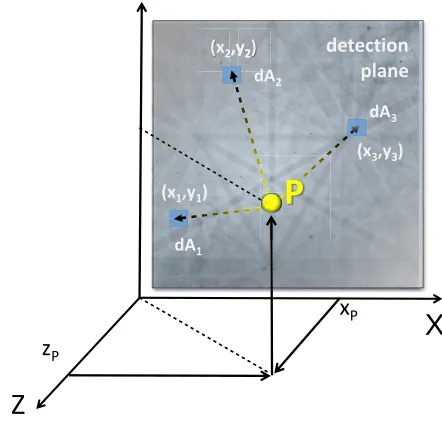
The accurate determination of the three-dimensional position of objects is connected to many measurement prob-lems in the experimental sciences and in technological appli-cations.1 Very often, however, the object of interest is not directly accessible. In such situations, we can still obtain directional measurements from known reference points and then triangulate the position of the object. This trivial princi-ple is illustrated in Fig.1, where measurements of the angles from the two reference points (x1,y1) and (x2,y2) to the point P would be sufficient to determine the three-dimensional coordinates (xP,yP, andzP) of that point, given that we know the reference distances in theXY-plane.
In this paper, we will discuss a generalized concept of position determination via triangulation, which we apply to determine the position of localized sources of radiation used in crystallography but which is also relevant to other applica-tions involving localized sources of waves. In our method, instead of performing direct angular measurements from iso-lated reference points, an extended two-dimensional detector area is designed to have a sensitivity which depends in a spe-cific way on the incident direction of the waves on each area elementdAon the detector surface. This angular sensitivity is encoded by the internal periodic structure of each area ele-ment, which can react to the specificwave-likeproperties of the incident radiation. As a result of diffraction effects inside each pixel, the detector displays for each pixel area element
dAan intensity related to the direction from the area element
dA to the source point. Each possible three-dimensional position of the source P relative to the detector defines a characteristic two-dimensional intensity pattern of the detec-tor area elements. In contrast to direct angular triangulation measurements, the individual measurement points by them-selves do not carry sufficient information to reconstruct the
position ofP. Instead, in the method discussed in this paper, P is determined by the combined 2D signal of all detector pixels dAnwhich is illustrated by the characteristic pattern
seen in the XY-plane in Fig. 1. A calibration procedure relates the three-dimensional position of the source atPand the corresponding projective two-dimensional features formed by the area elementsdAn. Summarizing the very
[image:1.612.324.545.464.677.2]gen-eral idea, the use of an area detector with internal periodic structure in the detector elements makes it possible to regis-ter additional information on the direction of the incoming
FIG. 1. Principle of determination of the source coordinates (xP,yP, andzP). The detector with area elementsdAnis reacting to diffraction effects of the waves from the source in the area element. Each area element at a specific position (xn,yn) on the detector is sensitive to thedirectionfrom the source to the area element. A triangulation procedure involving known diffraction features formed in the detector plane allows the source position to be determined.
a)Electronic mail: [email protected] b)
Electronic mail: [email protected]
radiation and to fix the spatial position of a source relative to a detector plane.
We now demonstrate a prototypical practical implemen-tation example of the diffractive ranging method we have discussed above. Our example is placed in the context of microstructural analysis methods in the scanning electron microscope (SEM), where the method of electron backscatter diffraction (EBSD) provides spatially resolved crystallo-graphic information.2,3EBSD is based on the measurement of Kikuchi diffraction patterns in a gnomonic projection on a planar screen placed near the sample.2As an accurate knowl-edge of the projection center is necessary to calibrate the angular coordinates of the Kikuchi pattern on the detector screen, a key problem in EBSD is the determination of the exact position of the electron beam spot relative to the detector.2–19
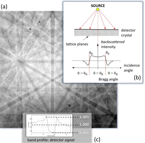
We have previously used a digital hybrid pixel detector, Timepix,20,21in a SEM to obtain Kikuchi patterns from crys-talline samples22by direct electron detection. Detailed inves-tigations revealed that the Timepix detector response exhibits an underlying diffraction pattern even in the total absence of diffraction effects from the sample (see Fig.
2(a)). Strikingly, the observed patterns have a negative inten-sity distribution relative to what is usually observed for back-scattered electrons from the sample in the SEM. As we will show by comparison to simulations, these patterns can be interpreted as electron channeling patterns23 which are formed not by the sample but in the Timepixdetectorcrystal itself. The observation of these “detector diffraction patterns” (DDP) means that the Timepix detector can serve as an array of directionally sensitive pixels in the context of the diffractive triangulation principle introduced above.
The basic physical mechanism leading to the detector diffraction patterns is as follows: In the SEM, electrons back-scattered from the sample travel towards the Timepix
detector, which is made from a Si wafer that is cut in the (111) orientation. On each separate pixel of the detector, the electrons thus impinge from a specific angular direction (see Fig. 2(b)). Due to multiple electron reflection at the lattice planes of the silicon detector crystal, the incoherent back-scattering probability and penetration depth of the incident electrons is changed when they are near the Bragg angle. This is due to the preferential excitation of Bloch waves that are localized on lattice planes or between them.23 In corre-spondence with the incident beam diffraction effects, the excitation of electron-hole pairs in each silicon pixel element (the measured signal) will be varying as a function of inci-dence angle. Because less electrons penetrate into the crystal when there is a large backscattered signal, the observed DDP is inversely proportional to the backscattered intensity, com-pare Figs.2(b)and2(c). The electron channeling effect thus provides a one-to-one relationship between pixel position on the detector and the direction towards the source point on the sample as was discussed above. Because the specific geomet-ric projection of the DDP features on the detector depends on the position (xP,yP,zP) of the source point, a calibrated DDP can thus provide these coordinates relative to the screen.
The calibration procedure for each measured DDP involves a quantitative comparison with theoretical Kikuchi pattern simulations, which depend on the detected electron energy, the source point position, and the orientation of the silicon detector crystal structure with respect to the detector surface plane; see Fig.3for an example.
[image:2.612.54.294.494.731.2]The best fit orientation and projection center coordinates were determined by the optimization of the normalized cross-correlation coefficient24 r (0<jrj<1) between the measured DDPs and series of corresponding simulations. We used the Nelder-Mead simplex method25 to find the local maximum of the cross-correlation coefficient between exper-iment and simulations, with start parameters near an orienta-tion obtained by a convenorienta-tional indexing procedure based on the Hough transform.26 For the dynamical electron diffrac-tion simuladiffrac-tions27 and the best-fit optimizations, we applied the software ESPRIT DynamicS (Bruker Nano, Berlin). In the optimization procedure, the simulated Kikuchi patterns are reprojected from stored master data according to the cur-rent values of the projection parameters, then the cross-correlation coefficient is calculated, and new updated
FIG. 2. Measured signal on the Timepix detector. Pixel(angle)-dependent electron absorption measured on the TimePix detector. Electron channeling effect of electron waves incident on a single-crystalline detector.
FIG. 3. Determination of the source point coordinates from an inverted detector diffraction pattern. The measured pattern for 12 keV beam energy (a) is compared to a dynamical diffraction simulation in (b). The best-fit coordinates of the electron source were (xP,yP, andzP)¼(6313lm, 5753
[image:2.612.348.529.598.695.2]projection parameters are chosen for the next iteration according to the simplex approach.25As an example of a fit result, in Fig.3we obtain a maximum value ofr¼0.71 for the cross-correlation coefficient between the experimental DDP and a simulated DDP for the electron source at (xP,yP, andzP)¼(6313lm, 5753lm, and 6416lm) in the detector coordinate system (Fig.1).
In order to determine the 3D position of the electron source via the Timepix detector, we need to know the exact orientation of the silicon crystal structure comprising the detector device. Since we know that the detector crystal is from commercial quality Si wafers with known lattice con-stant, we can assume a fixed, despite initially unknown, ori-entation for the detector. The crystal oriori-entation of the sensor material is fixed for the lifetime of the individual detector and is determined by manufacturing variations when cutting the Si crystal into the shape needed for the device. Mathematically, the orientation of the Si crystal structure relative to the edges of the detector can be described by Euler angles ð/1;U;/2Þwhich parametrize a
rotation sequence around moving ZXZ-axes in the Bunge convention.28The determination of the fixed detector crystal orientation is inherently limited by the precision of the same type of methods that are also used determine local crystal orientation in an actual sample. We have chosen here to esti-mate the fixed detector orientation as the mean orientation determined from a series of measurements which consist of moving the electron beam in a regular two-dimensional grid over the surface of a sample that shows no backscattering diffraction pattern.
In order to estimate the fixed Si detector crystal orienta-tion, we varied both the orientation and the projection center position of all measured DDPs in a 1010 grid map with approx. 10lm horizontal step size from an HfO2film which showed no backscattered Kikuchi patterns at 20 keV primary beam energy. Using MTEX,29the best-fit fixed detector crys-tal orientation was approximated as the mean orientation from all measurements in the map and resulted in Euler angles of (/1¼179:95;U¼54:53;/2¼45:15). This
corresponds to a misorientation angle of 0.24away from an ideal orientation with a (1 1 1) detector surface normal and
½110parallel to the horizontal edge of the detector. The size of the deviation is compatible with the overall manufacturing uncertainties. In order to estimate the orientation spread that results from parameter correlation effects the optimization procedure, we calculated an average misorientation of 0.04 with respect to the mean orientation when both the orienta-tion of the Si detector crystal and the projecorienta-tion center of the DDP are left to vary. In the analysis of the subsequent meas-urements, we then fixed the Timepix detector crystal orienta-tion at the Euler angles obtained in the procedure discussed above, and we allowed only the projection center coordinates to vary.
As a first test of the precision of the projection center determination, we repeated the optimization procedure for the measurement of the 1010 map discussed above, but now using the estimated fixed Timepix crystal orientation. Analyzing the mean values and standard deviations in rows and columns of the measured grid, which was assumed to be aligned with the x-axis of the detector, and taking into
account a sample tilt of about 73, we obtain an estimate of about 2.0lm for the precision of the projection center coor-dinates. A comparison to simulated perfect reference data showed that about half of this value is already due to the cur-rent sensitivity of our pattern fit optimization approach for the image resolution of 256256 pixels. We also estimated that the energy at which the DDP is simulated has to be cor-rect to within about 0.5 keV in order for the final fit result to stay in the limits stated above. The value of 2.0 lm can be put into perspective by comparison to previous studies of precision in the EBSD method.4,5,8,12–14 In these investiga-tions, minimum error values near 0.2%–0.5% of the pattern width (100lm) are quoted for the precision of the current standard methods of projection center determination. The error estimated for the setup used here indicates an improve-ment by at least one order of magnitude and is approaching values claimed for high-precision shadow-grid methods (0.5
lm14) and for the moving screen technique combined with image correlation (theoretically<1lm, but larger in practice due to optical and mechanical effects13). The improvement in projection center precision which we estimate here for a detector device with 256256 pixels is very promising when we take into account that the conventional strain deter-mination is carried out using pattern resolutions in the order of 10001000 pixels. Corresponding improvements in the precision of the projection center determination by DDPs can be expected if the resolution of the detector chip is increased to similar values, also considering the total absence of additional optical distortions in the monolithic direct electron detection device and no demand for extra cal-ibration hardware like in the shadow-casting approaches.
In the remaining part of this Letter, we demonstrate the self-calibrating property of the Timepix detector, which in principle imprints, via the DDP effect, a watermark-like intensity distribution on all measured EBSD patterns. This can be used to calibrate an experimental Kikuchi pattern without using any other information other than the pattern itself and the instrumentally fixed detector crystal orienta-tion. To this end, in Fig. 4, we present a Kikuchi pattern measurement at 25 keV, using a Si(001) sample covered by 10 nm of nanocrystalline HfO2, which for Kikuchi pattern formation can be considered as amorphous. The upper part of Fig. 4 shows the measured pattern (a) and an inverted copy (b) of the same pattern. The lower part of Fig.4shows on the right side (d) the best-fit simulation for the pattern center position from the negative of the total experimental pattern. The projection center was determined with a best fit
sample. The orientation was determined with a best fit r -value ofr¼0.43, again showing a selective minimum. The lower values ofrin Fig.4compared to the fit in Fig.3are due to the mixture of two patterns, where it is actually bene-ficial that one of the patterns is negative since this will tend to stabilize the optimization procedure for each partial pat-tern. In future applications, it could be envisaged to combine both optimizations in a simultaneous fit procedure. In this pilot experiment, the relative mixture of sample and detector diffraction could be tuned to about 50% each by adjusting the energy of the electron beam and the thickness of the cov-ering HfO2 film. In a conventional experiment involving high-quality crystalline surfaces, the DDP contribution is of the order of parts of a percent (see Fig.2(c)). However, as the detector diffraction contribution is in principle known, the extraction of the DDP watermark pattern from the mea-sured Kikuchi pattern should be possible by image process-ing techniques like template matching or similar approaches.24 Also, one can envisage the use of regular arrays of amorphous reference marks on the sample surface for calibration measurements.
The mode of measurement presented here should also be applicable to other wave sources, given that the source size is sufficiently small compared to the solid angle covered by the detector. For an electron beam in the SEM, the source size is in the order of 0.1lm for EBSD.30At distances near 5000lm, this corresponds to an angular range of about 0.001 (2105rad). As the width of the detector Kikuchi
band features is on the order of several pixels of 55lm dimension, in our case, we can still neglect the influence of the source size which will otherwise lead to a blurring of the diffraction features.
In summary, we have discussed a principle of diffractive triangulation of localized radiative sources using two-dimensional crystalline detectors. As an example, we have demonstrated the application of this principle for the deter-mination of the position of a source of electrons which are backscattered from the surface of a sample in a scanning electron microscope. The results presented here are an initial step towards a more accurate determination of the projection center of Kikuchi and other diffraction patterns, which will carry an inherent watermark of the projection center when measured with crystalline active-pixel detectors like Timepix or similar devices.31 Apart from the prototypical example discussed in this paper, the general diffractive trian-gulation method presented here can be imagined in applica-tions to various types of particle, electromagnetic, or other waves, provided that the technological detector design is modified accordingly.
We thank Joseph Roberts, University of Liverpool, for providing us with the HfO2 sample, and we thank NPL for partial funding of S.V.’s Ph.D. studentship. The experimental data presented in this paper are available at http://dx.doi.org/ 10.15129/93155663-d967-4ebb-81e2-0964befe80b6. This work was carried out with the support from EPSRC Grant No. EP/ J015792/1 and through support from a Carnegie Trust Research Incentive Grant No. 70483.
1
O. D. Faugeras, Three-Dimensional Computer Vision: A Geometric
Viewpoint, Artificial Intelligence Series (MIT Press, Cambridge, USA, 1993).
2
Electron Backscatter Diffraction in Materials Science, edited by A. J. Schwartz, M. Kumar, and B. L. Adams (Kluwer Academic/Plenum Publications, New York, 2000).
3O. Engler and V. Randle,Introduction to Texture Analysis: Macrotexture,
Microtexture, and Orientation Mapping, 2nd ed. (CRC Press, Boston, MA, USA, 2009).
4
J. A. Venables and R. Bin-Jaya, “Accurate microcrystallography using electron back-scattering patterns,”Philos. Mag.35, 1317–1332 (1977). 5
S. Biggin and D. J. Dingley, “A general method for locating the X-ray source point in Kossel diffraction,” J. Appl. Crystallogr. 10, 376–385 (1977).
6
D. J. Dingley, M. Longden, J. Weinbren, and J. Alderman, “Online analy-sis of electron back scatter diffraction patterns. 1. Texture analyanaly-sis of zone refined polysilicon,” Scanning Microsc.1, 451–456 (1987).
7K. Z. Baba-Kishi, “Measurement of crystal parameters on backscatter Kikuchi diffraction patterns,”Scanning20, 117–127 (1998).
8N. C. K. Lassen and J. B. Bilde-Sørensen, “Calibration of an electron back-scattering pattern set-up,”J. Microsc.170, 125–129 (1993). 9
N. C. K. Lassen, “Source point calibration from an arbitrary electron back-scattering pattern,”J. Microsc.195, 204–211 (1999).
10
D. A. Carpenter, J. L. Pugh, G. D. Richardson, and L. R. Mooney, “Determination of pattern centre in EBSD using the moving-screen technique,”J. Microsc.227, 246–247 (2007).
11
G. Nolze, “Image distortions in SEM and their influences on EBSD meas-urements,”Ultramicroscopy107, 172–183 (2007).
12
T. B. Britton, C. Maurice, R. Fortunier, J. H. Driver, A. P. Day, G. Meaden, D. J. Dingley, K. Mingard, and A. J. Wilkinson, “Factors affect-ing the accuracy of high resolution electron backscatter diffraction when using simulated patterns,”Ultramicroscopy110, 1443–1453 (2010). 13
[image:4.612.54.296.53.323.2]C. Maurice, K. Dzieciol, and R. Fortunier, “A method for accurate local-isation of EBSD pattern centres,”Ultramicroscopy111, 140–148 (2011). FIG. 4. Backscattered electron diffraction measurement at 25 keV obtained
from a film of 10 nm HfO2 on Si(001) using a Timepix detector. (a)
Measurement containing simultaneously a detector diffraction pattern (DDP, dark bands) together with a backscatter Kikuchi pattern (BKP, light bands) of the silicon sample. (b) Negative of the left pattern (d) Best-fit simulation of the pattern structure corresponding to the DDP. This gives the projection point (xP,yP, andzP). (c) Best-fit simulation of the BKP corresponding to the sample orientation of (/1¼179:95;U¼19:93;/2¼215:59),
14K. Mingard, A. Day, C. Maurice, and P. Quested, “Towards high accuracy calibration of electron backscatter diffraction systems,”Ultramicroscopy 111, 320–329 (2011).
15J. Basinger, D. Fullwood, J. Kacher, and B. Adams, “Pattern center
deter-mination in electron backscatter diffraction microscopy,” Microsc.
Microanal.17, 330–340 (2011). 16
J. Alkorta, “Limits of simulation based high resolution EBSD,”
Ultramicroscopy131, 33–38 (2013). 17
F. Ram, S. Zaefferer, and D. Raabe, “Kikuchi bandlet method for the accu-rate deconvolution and localization of kikuchi bands in kikuchi diffraction patterns,”J. Appl. Crystallogr.47, 264–275 (2014).
18Y. H. Chen, S. U. Park, D. Wei, G. Newstadt, M. A. Jackson, J. P.
Simmons, M. De Graef, and A. O. Hero, “A dictionary approach to electron backscatter diffraction indexing,”Microsc. Microanal.21, 739–752 (2015). 19
T. Britton, J. Jiang, Y. Guo, A. Vilalta-Clemente, D. Wallis, L. Hansen, A. Winkelmann, and A. Wilkinson, “Tutorial: Crystal orientations and EBSD—Or which way is up?,”Mater. Charact.117, 113–126 (2016). 20
X. Llopart, R. Ballabriga, M. Campbell, L. Tlustos, and W. Wong, “Timepix, a 65k programmable pixel readout chip for arrival time, energy and/or photon counting measurements,” Nucl. Instrum. Methods Phys., Res. Sect. A581, 485–494 (2007).
21
See http:\\medipix.web.cern.ch for information about the Medipix collaboration.
22S. Vespucci, A. Winkelmann, G. Naresh-Kumar, K. P. Mingard, D.
Maneuski, P. R. Edwards, A. P. Day, V. O’Shea, and C. Trager-Cowan,
“Digital direct electron imaging of energy-filtered electron backscatter dif-fraction patterns,”Phys. Rev. B92, 205301 (2015).
23
D. C. Joy, D. E. Newbury, and D. L. Davidson, “Electron channeling patterns in the scanning electron microscope,” J. Appl. Phys. 53, R81 (1982).
24
R. C. Gonzalez and R. E. Woods, Digital Image Processing, 3rd ed.
(Prentice Hall, 2007).
25W. H. Press, S. A. Teukolsky, W. T. Vetterling, and B. P. Flannery,
Numerical Recipes: The Art of Scientific Computing, 3rd ed. (Cambridge University Press, New York, NY, USA, 2007).
26
N. C. Krieger Lassen, “Automatic crystal orientation determination from EBSPs,”Micron and Microscopica Acta23, 191–192 (1992).
27A. Winkelmann, C. Trager-Cowan, F. Sweeney, A. P. Day, and P.
Parbrook, “Many-beam dynamical simulation of electron backscatter dif-fraction patterns,”Ultramicroscopy107, 414–421 (2007).
28A. Morawiec,Orientations and Rotations(Springer, 2003).
29F. Bachmann, R. Hielscher, and H. Schaeben, “Texture analysis with
MTEX—A free and open source software toolbox,”Solid State Phenom.
160, 63–68 (2010).
30S. Zaefferer, “On the formation mechanisms, spatial resolution and inten-sity of backscatter Kikuchi patterns,” Ultramicroscopy 107, 254–266 (2007).
31