Rochester Institute of Technology
RIT Scholar Works
Theses Thesis/Dissertation Collections
4-1-2011
Design and synthesis of a high-performance,
hyper-programmable DSP on an FPGA
Stephen Nichols
Follow this and additional works at:http://scholarworks.rit.edu/theses
This Thesis is brought to you for free and open access by the Thesis/Dissertation Collections at RIT Scholar Works. It has been accepted for inclusion in Theses by an authorized administrator of RIT Scholar Works. For more information, please [email protected].
Recommended Citation
Design and Synthesis of a High-Performance,
Hyper-Programmable DSP on an FPGA
by
Stephen W. Nichols
A Thesis Submitted in Partial Fulfillment of the Requirements for the Degree of Master of Science in Computer Engineering
Supervised by
Assistant Professor Dr. Andres Kwasinski Department of Computer Engineering
Kate Gleason College of Engineering Rochester Institute of Technology
Rochester, New York April 2011
Approved By:
Dr. Andres Kwasinski
Assistant Professor, Department of Computer Engineering Primary Adviser
Dr. Marcin Lukowiak
Assistant Professor, Department of Computer Engineering
Dr. Antonio F. Mondragon
Thesis Release Permission Form
Rochester Institute of Technology
Kate Gleason College of Engineering
Title: Design and Synthesis of a High-Performance, Hyper-Programmable
DSP on an FPGA
I, Stephen W. Nichols, hereby grant permission to the Wallace Memorial Library to
repro-duce my thesis in whole or in part.
Stephen W. Nichols
Abstract
In the field of high performance digital signal processing, DSPs and FPGAs provide the
most flexibility. Due to the extensive customization available on FPGAs, DSP algorithm
implementation on an FPGA exhibits an increased development time over programming a
processor. Because of this, traditional DSPs typically yield a faster time to market than an
FPGA design. However, it is often desirable to have the ASIC-like performance that is
at-tainable through the additional customization and parallel computation available through an
FPGA. This can be achieved through the class of processors known as hyper-programmable
DSPs.
A hyper-programmable DSP is a DSP in which multiple aspects of the architecture
are programmable. This thesis contributes such a DSP, targeted for high-performance and
realized in hardware using an FPGA. The design consists of both a scalar datapath and a
vector datapath capable of parallel operations, both of which are extensively customizable.
To aid in the design of the datapaths, graphical tools are introduced as an efficient way to
modify the design. A tool was also created to supply a graphical interface to help write
instructions for the vector datapath. Additionally, an adaptive assembler was created to
convert assembly programs to machine code for any datapath design.
The resulting design was synthesized for a Cyclone III FPGA. The synthesis resulted in
a design capable of running at 135MHz with 61% of the logic used by processing elements.
Benchmarks were run on the design to evaluate its performance. The benchmarks showed
similar performance between the proposed design and commercial DSPs for the simple
Contents
Abstract . . . iii
Glossary . . . xi
1 Introduction. . . 1
1.1 Motivation . . . 1
1.2 Contribution . . . 3
1.3 Thesis Organization . . . 3
2 Related Work . . . 4
2.1 Hyper-Programmable Processors . . . 4
2.1.1 Altera Nios II . . . 4
2.1.2 EPIC . . . 6
2.1.3 CUSTARD . . . 8
2.2 Transport Triggered Architecture . . . 10
2.2.1 FFTTA . . . 10
2.2.2 TTA-based Co-design Environment . . . 11
2.3 NoC-based Datapaths . . . 12
2.4 Commercial DSPs . . . 13
2.4.1 Analog Devices TigerSHARC . . . 14
2.4.2 Texas Instruments TMS320C6746 . . . 15
3 Design . . . 17
3.1 Vector Processor . . . 18
3.1.1 Vector Datapath . . . 19
3.1.2 Status Table . . . 26
3.1.3 Operand Control . . . 28
3.2 Scalar Processor . . . 29
3.2.2 Instruction Decode . . . 31
3.2.3 Processing Elements . . . 32
4 Toolset . . . 35
4.1 Vector Datapath Designer . . . 36
4.1.1 User Interface . . . 36
4.1.2 Datapath Generation . . . 38
4.2 Scalar Datapath Designer . . . 39
4.2.1 User Interface . . . 39
4.2.2 Datapath Generation . . . 42
4.3 Vector Datapath Programmer . . . 43
4.4 Scalar Assembler . . . 47
5 Test Setup . . . 50
5.1 Simulation Environment . . . 51
5.2 Hardware Environment . . . 52
5.3 Example Vector Datapath . . . 55
5.4 Example Scalar Datapath . . . 57
6 Results. . . 59
6.1 Synthesis . . . 59
6.2 Benchmarks . . . 62
6.2.1 Vector Search . . . 63
6.2.2 Vector Multiply . . . 66
6.2.3 FFT . . . 68
6.2.4 FIR . . . 72
6.3 Power Consumption . . . 78
7 Conclusions . . . 81
7.1 Future Work . . . 82
Bibliography . . . 84
A Header definitions . . . 87
B Benchmark Programs . . . 89
List of Figures
1.1 DSP implementation spectrum . . . 2
2.1 Block diagram of the Nios II architecture [7] . . . 5
2.2 Block diagram of C2H accelerated Nios II [3] . . . 6
2.3 Organization of EPIC architecture [14] . . . 7
2.4 Organization of CUSTARD architecture [16] . . . 8
2.5 Organization of a TTA [15] . . . 10
2.6 Block diagram of the FFTTA architecture [23] . . . 11
2.7 TCE’s graphical processor designer tool [26] . . . 12
2.8 Block diagram of the IPNoSys architecture [19] . . . 13
2.9 Block diagram of the TigerSHARC architecture [8] . . . 14
2.10 Block diagram of the TMS320C6746 DSP architecture [31] . . . 15
3.1 Design overview . . . 17
3.2 Vector processor overview . . . 18
3.3 Example vector datapath . . . 19
3.4 Bus definition . . . 20
3.5 Bus flow-control bits . . . 20
3.6 Header word definitions . . . 20
3.7 Wrapper takes a packet (top) and simplifies it (bottom) for a processing element . . . 22
3.8 Picking off local opcode bits . . . 23
3.9 Picking off local parameter words . . . 23
3.10 Bidirectional bus register . . . 25
3.11 Vector datapath status table . . . 26
3.12 Timing diagram of a status table entry . . . 27
3.13 Overview of operand control module . . . 28
3.14 Scalar processor overview . . . 29
3.15 Scalar processor pipeline flow . . . 30
3.17 Instruction decode design . . . 32
3.18 Scalar opcode format . . . 32
3.19 Scalar processing element - adder . . . 33
3.20 Scalar processing element - vector datapath control . . . 34
4.1 Design flow . . . 36
4.2 Screenshot of Vector Datapath Designer tool . . . 37
4.3 Generics in FFT element . . . 38
4.4 Screenshot of Scalar Datapath Designer tool . . . 40
4.5 Entity declaration for adder element . . . 41
4.6 Screenshot of Vector Datapath Programmer tool . . . 44
4.7 FFT opcode definitions . . . 45
4.8 Assembly from example vector instruction . . . 47
4.9 Screenshot of Scalar Assembler tool . . . 47
4.10 Example assembly program . . . 48
5.1 Overview of the test setup . . . 50
5.2 Overview of the simulation environment . . . 51
5.3 Overview of the hardware test environment . . . 53
5.4 Example vector datapath . . . 55
5.5 Band-pass and band-stop windows . . . 56
6.1 Logic elements (left) and RAM (right) used by the design . . . 60
6.2 Logic elements (left) and RAM (right) used by the vector processor . . . . 61
6.3 Logic elements (left) and RAM (right) used by the scalar processor . . . 61
6.4 Vector Search instruction . . . 63
6.5 Assembly listing for 2k vector search . . . 64
6.6 Execution time for 2048 element search benchmark . . . 65
6.7 Vector Multiply instruction 1 . . . 66
6.8 Vector Multiply instruction 2 . . . 66
6.9 Execution time for 2048 element vector multiply benchmark . . . 67
6.10 Accuracy of 2048 element vector multiply . . . 68
6.11 FFT instruction . . . 69
6.12 Execution time for 2048 point FFT benchmark . . . 70
6.13 Execution time for 1024 point FFT benchmark . . . 70
6.15 Accuracy of 2048 point FFT . . . 72
6.16 Overlap-save filtering,y(n) =x(n)∗h(n)[11] . . . 73
6.17 FIR instruction 1 . . . 73
6.18 FIR instruction 2 . . . 74
6.19 FIR instruction 3 . . . 74
6.20 FIR instruction 4 . . . 75
6.21 Execution time for N=10000, M=10 FIR benchmark . . . 76
6.22 Execution time for N=10000, M=100 FIR benchmark . . . 77
6.23 Execution time for N=10000, M=512 FIR benchmark . . . 77
6.24 Accuracy of N=10000, M=100 FIR . . . 78
6.25 Power consumption of each DSP . . . 79
List of Tables
2.1 Nios II 256-point FFT performance [3] . . . 6
3.1 List of port signals for VHDL processing element cores . . . 24
3.2 Port signals for VHDL scalar processing elements . . . 33
4.1 Outline of Vector Datapath Designer VHDL generation . . . 38
4.2 Additional port signals for VHDL scalar instruction fetch modules . . . 40
4.3 Outline of Scalar Datapath Designer VHDL generation . . . 42
4.4 Vector Datapath Programmer display directives . . . 46
5.1 UART to DSP interface commands . . . 54
5.2 Elements in the example scalar datapath . . . 57
6.1 Resource usage of synthesized design . . . 59
Glossary
ALU Arithmetic Logic Unit.
ASIC Application-Specific Integrated Circuit.
DSP Digital Signal Processing.
DSP Digital Signal Processor.
FFT Fast Fourier Transform.
FIFO First In First Out.
FIR Finite Impulse Response.
FPGA Field Programmable Gate Array.
IC Integrated Circuit.
I/O Input/Output.
MATLAB MATrix LABoratory.
MEX Matlab EXecutable.
NoC Network on Chip.
NOP No Operation.
OFDM Orthogonal Frequency-Division Multiplexing.
RAM Random Access Memory.
SDR Software Defined Radio.
SIMD Single Instruction, Multiple Data.
SNR Signal to Noise Ratio.
TTA Transport Triggered Architecture.
Chapter 1
Introduction
1.1
Motivation
In the field of high performance digital signal processing (DSP), digital signal processors
(DSPs) and field programmable gate arrays (FPGAs) provide the most flexibility. Due
to the extensive customization available on FPGAs, DSP algorithm implementation on an
FPGA exhibits an increased development time over programming a DSP. Because of this,
traditional DSPs typically have a faster time to market than an FPGA design. However, it is
often desirable to have the increased performance that is attainable through the additional
customization and parallel computation available through an application-specific integrated
circuit (ASIC) or FPGA. It would therefore be advantageous to introduce a new class of
processor called hyper-programmable DSPs. A traditional spectrum of DSPs consisting of
four categories was given in [27]. Figure 1.1 depicts this spectrum with the addition of
hyper-programmable DSPs. The vertical axis in the diagram depicts the range of flexibility
achievable through software. As programmability increases, cost and development time
decrease. The horizontal axis shows the range of specialization of each technology. As
specialization increases, performance and efficiency also increase. By comparing these
General Purpose Processor
Programmable DSP
Reconfigurable Hardware
ASIC
Specialization Hyper-Programmable
DSP
P
ro
g
ra
m
m
a
b
ili
ty
Figure 1.1: DSP implementation spectrum
The term “hyper-programmable” has been used to describe an architecture where
mul-tiple aspects of the architecture are programmable, rather than just supporting a
program-ming model [12]. In other words, a hyper-programmable processor’s datapath is
customiz-able, although not necessarily at run-time. Such an architecture can be realized through the
use of a customizable processor programmed on an FPGA.
One DSP application that requires high performance, flexibility, and low power usage
is software-defined radio (SDR). Although standard DSP processors are flexible, they often
are unable to achieve high performance with low power dissipation [13]. ASIC processors
do not provide the flexibility required to support variations of implemented wireless
algo-rithms as is expected from SDRs [13]. A hyper-programmable DSP, on the other hand, can
be customized to meet these requirements. Additionally, the ability to quickly reconfigure
this type of processor makes it an excellent fit for the ever-changing domain of wireless
1.2
Contribution
This thesis contributes a high-performance, hyper-programmable DSP design realized in
hardware using an FPGA. To achieve high performance, the design consists of both a scalar
datapath and vector datapath capable of parallel operations. Both datapaths are extensively
customizable at compile-time, thus providing hyper-programmability. To aid in the design
of the datapaths, graphical tools were developed as an efficient way to modify the design. A
tool was also created to supply a graphical interface to help write instructions for the vector
datapath. Additionally, an adaptive assembler was created to convert assembly programs
to machine code for any datapath design.
1.3
Thesis Organization
The remainder of this thesis is organized as follows. Chapter 2 lays the groundwork for the
thesis by discussing other processor designs related to the proposed DSP. Chapter 3 goes
into detail on the design and architecture of the proposed processor. The supporting toolset
consisting of datapath design tools, a graphical programming tool, and an assembler is
presented in Chapter 4. Chapter 5 provides details about both the simulation and hardware
testbench environments. The results of the design synthesis along with performance of a
set of benchmark programs are given and discussed in Chapter 6. Chapter 7 concludes this
Chapter 2
Related Work
One realization of a hyper-programmable processor is through the use of a customizable
soft processor core on an FPGA. Examples of both commercial and academic
implementa-tions of this are presented in the following section. TTA (Transport Triggered Architecture)
processors are then discussed as an architecture that can provide a foundation for
hyper-programmability. The IPNoSys architecture, which uses packets to encapsulate instructions
and data to be processed in an NoC (Network-on-Chip) datapath, is then presented. Lastly,
an overview of commercial high-performance and low-power DSPs is given.
2.1
Hyper-Programmable Processors
2.1.1
Altera Nios II
The Nios II is a 32-bit general-purpose RISC processor core designed by Altera for use
in FPGA designs [7]. A block diagram of the processor is depicted in Figure 2.1. The
gray sections of the figure represent optional modules while the white sections represent
required ones.
As shown in the figure, there are a variety of optional modules to choose from when
customizing the Nios II. A number of the options are used to enhance memory
opera-tions through caches and memory management modules. If context switching is important,
Exception Controller Internal Interrupt Controller Arithmetic Logic Unit General Purpose Registers Control Registers Nios II Processor Core
[image:18.612.117.507.89.377.2]reset clock JTAG interface to software debugger Custom I/O Signals irq[31..0] JTAG Debug Module Program Controller & Address Generation Custom Instruction Logic Data Bus Tightly Coupled Data Memory Tightly Coupled Data Memory Data Cache Instruction Cache Instruction Bus Tightly Coupled Instruction Memory Tightly Coupled Instruction Memory cpu_resetrequest cpu_resettaken Memory Management Unit Translation Lookaside Buffer Instruction Regions Memory Protection Unit Data Regions External Interrupt Controller Interface eic_port_data[44..0] eic_port_valid Shadow Register Sets
Figure 2.1: Block diagram of the Nios II architecture [7]
performance, however, is through the use of custom instructions. The Nios II architecture
supports up to 256 user-defined custom instructions. The logic for the custom instructions
connects directly to the processor’s ALU, which allows hardware operations to be accessed
and used exactly like native instructions. [7]
In addition to the custom instructions, unlimited memory mapped hardware
accelera-tors can be added to the system. Acceleraaccelera-tors can directly access memory and other system
resources which yields high bandwidth. Hardware accelerators can be created manually
using VHDL or automatically using the Nios II C-to-Hardware Acceleration (C2H)
Com-piler. [7]
The C2H Compiler takes specified portions of the C code to be run on the Nios II and
creates logic that accelerates software algorithms [5]. This allows the performance of Nios
II programs to be significantly improved without any manual logic design. An example of
[3]. The resulting hardware accelerator is depicted in Figure 2.2. As shown, the accelerator
logic has direct memory access to achieve higher performance.
Nios II
SDRAM Calculation
Read Buffer
Calculation Write Buffer BufferRAM1
BufferRAM2
FFT Accelerator
Figure 2.2: Block diagram of C2H accelerated Nios II [3]
To demonstrate the performance speedup, results from both the original and optimized
designs running at 100MHz were given in [3]. The benchmark computed the FFT algorithm
on 256 points of real data. The results from both designs are shown in Table 2.1. From
these results, it can be seen that the C2H compiler can provide a significant performance
improvement while foregoing much additional development time.
Cycles Execution Time Speedup
Software Only 87,767 877.675µs 1
Hardware Accelerated 5,272 52.719µs 16.65
Table 2.1: Nios II 256-point FFT performance [3]
2.1.2
EPIC
The Explicitly Parallel Instruction Computing (EPIC) processor is an implementation of
a hyper-programmable processor designed for academic exploration of various
perfor-mance/area tradeoffs. The design supports precompilation customization of the following
• number of ALU units
• number of general purpose registers
• number of predicate registers
• number of branch target registers
• number of registers each instruction can use
• number of instructions per issue
• width of datapath and registers
• functionality of ALU.
First Stage Pipeline Second Stage Pipeline To Main Memory
BTR LSU ALU 1
ALU N CMPU BRU
Write Back Unit Fetch
Decode Issue
Unit Register
[image:20.612.184.437.343.623.2]File
Figure 2.3: Organization of EPIC architecture [14]
As shown in 2.3, the datapath implementation is split into two pipeline stages. In the
Two operand registers for each instruction are fetched from the general purpose register
file. The second stage consists of a collection of execution and control units: arithmetic
and logic units (ALUs), a load/store unit (LSU), a comparison unit (CMPU), a branch unit
(BRU), and a branch target register (BTR). Because multiple instructions are issued
simul-taneously, several of these units can be used concurrently. The outputs of the computational
units are connected to the Write Back Unit to handle writing each result back to the register
file. [14]
EPIC programs are written in C and then compiled using a custom compiler. Along
with C code, information regarding specific processor customizations is fed as input to
the compiler. In addition to performing machine independent optimizations, the compiler
statically schedules instructions by performing dependence analysis and resource conflict
avoidance. This moves the complexity of controlling the usage of each resource from
hardware to the compiler. [14]
2.1.3
CUSTARD
FORWARDING
FORWARDING_BRANCH
CUSTOM EXECUTION
UNITS
FORWARDING_ALU REGISTER FILE READ PORTS REGISTER FILE
MEMORY ALU
FETCH WRITEBACK
R0 R0 R1
Rn
Rm
n REGISTERS m THREADS
CONTROL BRANCH DELAY LOAD STALL
Figure 2.4: Organization of CUSTARD architecture [16]
CUSTARD (CUStomizable Threaded Architecture) is a hyper-programmable processor
processor design, shown in Figure 2.4, is based on a four-stage pipelined architecture. By
providing multiple banks of registers, the register file adds support for multiple contexts
within the same processor hardware. Each context stores state information of registers,
the stack, and the program counter for each thread. Because the context switch happens
at the hardware level, multiple threads can be run concurrently with little to no overhead.
Additionally, context switches can be used to hide latency which normally causes a stall.
[16]
As a hyper-programmable processor, CUSTARD supports customizations at time of
synthesis of a number of parameters [16]:
• number of threads
• threading type (block or interleaved)
• custom instructions
• forwarding and interlock architecture
• number of registers
• number of register file ports
• register bitwidth.
CUSTARD programs are written in C and compiled using an optimizing compiler. In
addition to producing optimized machine code, the compiler also generates custom
instruc-tions using a technique dubbed “Similar Sub-Instrucinstruc-tions.” This technique finds instruction
datapaths that can be reused across similar portions of code. These datapaths are then added
as custom execution units to the processor in addition to updating the decoding logic to map
2.2
Transport Triggered Architecture
One architecture of interest is the Transport Triggered Architecture (TTA). A TTA is
pro-grammed by describing the transport of data between function units rather than just
oper-ations of function units. The general organization of a TTA is shown in Figure 2.5. As
depicted in the diagram, TTAs are organized as a set of functional units (FUs) and register
units (RUs). Each of the function units performs an operation as a consequence of data
being transported to one of its input ports. The result from the computation is then stored
on a register connected to its output port. The interconnection network provides the means
to transport data among functional and register units. The interconnect consists of one or
more busses whose operation is controlled by instruction words. Since instructions only
specify where to move data from and to, the entire instruction set consists of a single
in-struction: a move instruction. Because of its simple, modular design, a TTA provides an
excellent candidate for a hyper-programmable processor design. [15]
In s tr u c ti o n M e m o ry Instruction fetch unit Instruction decode unit In te rc o n n e c ti o n n e tw o rk FU-1 FU-2 FU-3 RU-1 RU-2 D a ta M e m o ry Central processing unit
Figure 2.5: Organization of a TTA [15]
2.2.1
FFTTA
One example of a customized TTA is the FFTTA processor which customizes a TTA to
efficiently perform the FFT algorithm. The general organization of the design is shown in
Figure 2.6. The interconnect network for the design consists of 18 busses used to provide a
units in the design include a complex adder, a complex multiplier, a data address generator,
a coefficient generator, a real adder, a load-store unit, a comparator unit, and a control
unit. The register units provide a total of twenty-three 32-bit general purpose registers. The
interconnection among function and register units was minimized on each bus to provide an
optimized architecture for the specific application. This results in reduced area and power
consumption without sacrificing any performance. [23]
DATA MEM LD_ST
RF1
RF9 RF8 RF7 RF6 RF10 RF11 RF5 RF4 RF3
LD_ST ADD
COGEN CMUL
CADD AG
CNTRL INSTR
MEM COMP
RF2
Figure 2.6: Block diagram of the FFTTA architecture [23]
2.2.2
TTA-based Co-design Environment
At Tampere University of Technology, TTAs have been the focus of a number of research
projects since 2003 [26]. Researchers at the university developed and maintain a toolset
for designing application specific processors based on the TTA architecture. This toolset is
called the TTA-based Co-design Environment (TCE). TCE provides a complete co-design
flow from C programs down to synthesizable VHDL and parallel program binaries. The
tools allow processor customization of the register files, function units, and the
interconnec-tion network. TCE includes graphical customizainterconnec-tion tools, processor generator, C compiler,
Figure 2.7: TCE’s graphical processor designer tool [26]
2.3
NoC-based Datapaths
Networks-on-Chip (NoC) enable parallel communication between cores using messages
encapsulated in packets. Typically an NoC design consists of a set of routers
intercon-nected with other routers and end nodes such as processor cores. Normally the routers
are only responsible for the data transmission. However, by adding processing elements to
the routers, the network becomes a datapath. The advantage of this architecture is that it
creates a modular and thus scalable design. [19]
The IPNoSys architecture is an example of a processor using an NoC-based datapath.
An overview of the design is shown in Figure 2.8. As shown in the diagram, the processor
consists of four memory banks (Mem), four memory access units (MAU), and sixteen
routing and processing units (RPU). [19]
Instructions and operands are read from memory and encapsulated in packets by an
MAU and injected into the datapath. Each packet is made up of multiple message words
consisting of header words, instruction words, operand words, and a terminator word. In
MAU 0,0 RPU 0,1 RPU 0,0 RPU 0,2 RPU 0,3 MAU 0,3 Mem Mem RPU 1,0 RPU 1,1 RPU 1,2 RPU 1,3 RPU 2,0 RPU 2,1 RPU 2,2 RPU 2,3 MAU 3,0 RPU 3,1 RPU 3,0 RPU 3,2 RPU 3,3 MAU 3,3 Mem Mem
Figure 2.8: Block diagram of the IPNoSys architecture [19]
back into memory. [19]
The RPUs are made up of a packet buffer, a crossbar switch, an ALU, and control
logic. As an RPU receives a packet, it places it into a packet buffer. If the packet has
any instruction words, the first instruction in the packet is then executed in the ALU. The
resulting value from the operation is then inserted into the packet as an operand for a future
instruction. The current instruction and associated operand words are then removed from
the packet. The packet is then routed to one of the neighboring RPUs where the next
instruction can be processed. This results in a packet flowing from RPU to RPU until the
final result is computed and written back to memory. [19]
2.4
Commercial DSPs
Since there are many DSPs commercially available targetting general purpose signal
pro-cessing, it makes sense to detail and compare a few. Two high-end DSPs with floating-point
• Performance optimized DSPs
• Power optimized DSPs.
2.4.1
Analog Devices TigerSHARC
The TigerSHARC DSP is described by Analog Devices as an “ultrahigh performance, static
superscalar processor optimized for large signal processing tasks and communications
in-frastructure” [8]. A block diagram of the architecture is shown in Figure 2.9.
L0 8 4 8 4 8 4 8 4 8 4 8 4 8 4 8 4 IN OUT HOST MULTI-PROC C-BUS ARB DATA 64 LINK PORTS JTAG PORT EXTERNAL PORT ADDR 32 6 SOC BUS DMA JTAG SDRAM CTRL EXT DMA REQ J-BUS DATA IAB PC BTB ADDR FETCH PROGRAM SEQUENCER COMPUTATIONAL BLOCKS J-BUS ADDR K-BUS DATA K-BUS ADDR I-BUS DATA I-BUS ADDR S-BUS DATA S-BUS ADDR INTEGER K ALU INTEGER J ALU 32 32
32-BIT × 32-BIT
DATA ADDRESS GENERATION
X REGISTER
FILE 32-BIT × 32-BIT MUL
ALU SHIFT
CLU 128 DAB
128 DAB 128 128 MEMORY BLOCKS A D
24M BITS INTERNAL MEMORY
4 × CROSSBAR CONNECT (PAGE CACHE)
A D A D A D
SOC I/F
Y REGISTER
FILE 32-BIT × 32-BIT
MUL ALU SHIFT CLU
[image:27.612.96.518.262.540.2]L1 IN OUT L2 IN OUT L3 IN OUT CTRL 8 CTRL 10 32 128 32 128 32 128 21 128 4 32-BIT × 32-BIT
Figure 2.9: Block diagram of the TigerSHARC architecture [8]
The design features dual computational blocks that support IEEE 32-bit single-precision
floating-point, extended-precision 40-bit floating point, and 8-, 16-, 32-, and 64-bit
fixed-point processing. Each computational block is composed of 32-bit registers, a multiplier,
an ALU, a shifter, and a Viterbi decoder. Compute instructions can be independently
is-sued to two modules within a compute block in a single cycle. This means that between
fixed-point arithmetic, SIMD (Single Instruction, Multiple Data) instructions can be used
to operate on eight 8-bit, four 16-bit, or two 32-bit words simultaneously. [8]
2.4.2
Texas Instruments TMS320C6746
The TMS320C6746 is a low-power DSP with support for floating-point computations. A
block diagram of the DSP core is shown in Figure 2.10.
.L1 .S1 .M1 .D1
Register File A Data Path A
.D2 .M2 .S2 .L2
Register File B Data Path B Instruction Decode 16/32-Bit Instruction Dispatch
SPLOOP Buffer Instruction Fetch IDMA
Program Memory Controller (PMC)
Data Memory Controller
(DMC)
Interrupt & Exception
Controller Power Control Unified
Memory Controller
(UMC)
External Memory Controller
(EMC) L2
Cache/ SRAM
L1P Cache/SRAM
[image:28.612.170.453.238.531.2]L1D Cache/SRAM
Figure 2.10: Block diagram of the TMS320C6746 DSP architecture [31]
The design features dual datapaths each with an ALU (.L), a shifter unit (.S), a
multi-ply unit (.M), and a data unit (.D). The ALU unit is capable of up to four single precision
additions every cycle or four double precision additions every two cycles. The shifter unit
provides support for two floating point reciprocal calculations per cycle. The multiplier can
perform two single precision multiplications per cycle or two double precision
Chapter 3
Design
The primary design objectives for the architecture are hyper-programmability and DSP
performance. To achieve hyper-programmability, the architecture must support the addition
and modification of computational blocks. To achieve high performance, the framework
around the computational blocks must be capable of processing instructions and moving
data quickly.
Vector Processor Scalar Processor
External Memory Interface External
Communication Interface
Vector Instructions
Status
Memory Access Instruction Memory
Instruction Fetch
Instruction Decode
Processing Elements
Memory Bank 0
Memory Bank 1
Memory Bank 2
Vector Datapath Operand
Control 0
Operand Control 1
Operand Control 2
[image:30.612.94.525.391.609.2]Status Table
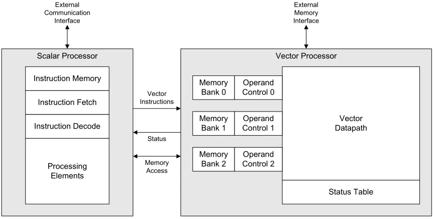
Figure 3.1: Design overview
The processor design is broken up into two main parts as shown in Figure 3.1. The
the computations. The scalar processor sequences instructions to the vector processor,
han-dles external communication, and performs non-vector operations. The scalar and vector
processors are discussed in detail in the following sections.
3.1
Vector Processor
In order to achieve the goal of high-performance, computation must dominate instruction
overhead. Because many DSP algorithms work on blocks of data at a time [33], the
over-head of instructions can be reduced by processing vectors up to thousands of data elements
long. An overview of the vector processor design is shown in Figure 3.2. Vector
instruc-tions are streamed by the scalar processor into the operand control modules. These modules
then create and transmit a packet containing instruction information and vector data into
the vector datapath. The vector datapath receives these packets and processes them to
pro-duce the computational result. The resulting vector data is then written back into a memory
bank. The status table keeps track of packets as they enter and exit the datapath, providing
useful information for scheduling upcoming instructions.
Vector Processor
Memory Bank 0
Memory Bank 1
Memory Bank 2
Vector Datapath
Operand Control 0
Operand Control 1
Operand Control 2
Status Table
External Memory Interface
Vector Datapath
Status Memory & Instruction Control 0
Memory & Instruction Control 1
Memory & Instruction Control 2
3.1.1
Vector Datapath
The vector datapath consists of three types of components: routing elements, processing
el-ements, and interconnects. Routing elements (depicted in Figure 3.3 as white polygons) are
used to direct packets through the datapath. Examples of routing elements include inputs,
multiplexers, demultiplexers, crossbar switches, forks, and outputs. Processing elements
perform the computations and thus are the fundamental building blocks of the datapath.
Examples of processing elements are shown in Figure 3.3 as gray polygons. Interconnects
represent data busses and are used to connect elements together. The interconnects are
depicted as lines in Figure 3.3 connecting the routing elements and processing elements.
Figure 3.3: Example vector datapath
Interconnects
Interconnects are used to transport packets containing instruction and vector data. This
happens on a 40-bit bus which is broken up into control and data sections as shown in
Figure 3.4. The bottom four bits are dedicated to controlling the flow of data across the
bus. The protocol used is a derivative of the Avalon Streaming Interface [6]. As shown in
Figure 3.5, one bit is used for reverse flow control and three bits are used for forward flow
until the flag is lowered. The “start of packet” flag is pulsed high during the same cycle as
the first valid word of the packet. Likewise, the “end of packet” flag is pulsed high during
the same cycle as the last valid word of the packet. The “data valid” flag is raised for every
word in the packet. Forward flow can be halted by lowering the “data valid” flag during
a packet’s transmission. The data portion was selected to be 36-bits wide since this is the
maximum width to which a Cyclone III block RAM can be configured [4].
0 1 2 3 4 5 6 7 8 9 10 11 12 13 14 15 16 17 18 19 20 21 22 23 24 25 26 27 28 29 30 31 32 33 34 35 36 37 38 39
Header / Data Ctrl
Figure 3.4: Bus definition
Start of Packet
End of Packet
Data Valid Hold Bit 0 Bit 1 Bit 2 Bit 3
Figure 3.5: Bus flow-control bits
Packets are made up of header words and vector data. Header words are used to store
opcode information, routing information, and writeback information. Each type of header
has a 4-bit header ID code associated with it as shown in Figure 3.6. The first word in a
packet must always be a header word. The last header word in the packet must have the ID
code 0xF indicating that the remaining words in the packet are all data. A bit definition of
each header word type is given in Figure A.1.
0 1 2 3 4 5 6 7 8 9 10 11 12 13 14 15 16 17 18 19 20 21 22 23 24 25 26 27 28 29 30 31 32 33 34 35
Header Data ID
o
Header
Exponent Imaginary Part Real Part
o
Data
Figure 3.6: Header word definitions
As shown in Figure 3.6, the chosen datatype is complex floating point. Since the
imaginary part. Floating point was selected in order to achieve a high dynamic range while
maintaining consistent precision. Although 32-bit floating point has become the single
precision standard, using fewer bits can still provide both sufficient precision and dynamic
range [17]. The real and imaginary parts of the floating point number are fractional
num-bers with one sign bit and fourteen precision bits. The exponent is a signed 6-bit number,
thus resulting in a dynamic range of26×20log
10(2) ≈385dB [17].
Processing Elements
Processing elements can perform a variety of computations on vector data including
• Vector addition
• Windowing
• Complex conjugation
• Element-wise multiplication
• Dot product
• Fourier transform
Each element has one or more operand inputs and generates a result on a single bus.
Pro-cessing elements can have parameterizable operations which are controlled by the opcode
section of the incoming packet. To maintain the desired performance, processing elements
must be capable of consuming and producing a new vector element every clock cycle.
Some processing elements, such as the FFT, might be too complex to complete in a single
clock cycle and thus need to be broken up into multiple pipeline stages.
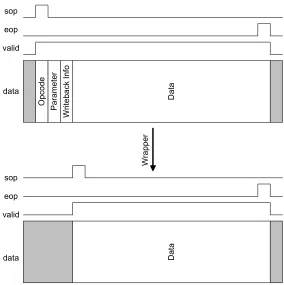
In order to provide a simple interface for processing element development, a wrapper
is placed around each processing element core. This wrapper parses the incoming packet
O p c o d e P a ra m e te r W ri te b a c k I n fo D a ta D a ta W ra p p e r sop eop valid data sop eop valid data
Figure 3.7: Wrapper takes a packet (top) and simplifies it (bottom) for a processing element
with adjusted flow-control signals to the processing element as shown in Figure 3.7. Header
words are delayed and used by the wrapper to reconstruct the outgoing packet.
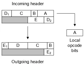
The wrapper is also responsible for presenting opcode bits and parameter words to the
processing element. Each processing element must predefine the number of opcode bits it
expects. When an instruction is issued, these opcode bits are concatenated to form one or
more header words with the opcode. When a wrapper module receives the packet, it takes
the lowest bits and shifts the opcode words to remove the local opcode and prepare the
packet for the next element. An example of this is shown in Figure 3.8.
In addition to receiving opcode bits, processing elements can also receive parameter
words. Parameter words are used for runtime parameters since opcode bits only provide
compile-time instruction. The wrapper uses bits in the opcode to enable or disable the
reception of parameter words. When enabled, the element can update any of its local
A B C D1
D2
E
B C D
E2
E1
A Incoming header
Outgoing header
Local opcode
bits
Figure 3.8: Picking off local opcode bits
Opcode Incoming header
Outgoing header
Local parameters Parameter A
Parameter B Parameter C
Opcode
Parameter C
[image:36.612.231.377.89.201.2]Parameter A Parameter B
Figure 3.9: Picking off local parameter words
remain unchanged since the wrapper registers all incoming parameters. After collecting
local opcodes, the wrapper erases any parameters locally used from the packet as shown in
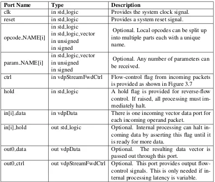
Figure 3.9. The port signals provided to a processing element by the wrapper are shown in
Table 3.1.
Since many processing elements operate on multiple input data vectors simultaneously,
it is important that the data sections of incoming packets are aligned in time. For example,
if a processing element begins to receive data for operand X but not for operand Y, then
it must stall the data on the X bus until data is also available on the Y bus. The wrapper
handles this by raising the reverse flow-control hold flag to pause the X bus until Y data
Port Name Type Description
clk in std logic Provides the system clock signal. reset in std logic Provides a system reset signal.
opcode NAME[i]
in std logic
Optional. Local opcodes can be split up into multiple parts each with a unique name.
in std logic vector in unsigned in signed
param NAME[i]
in std logic vector
Optional. Any number of parameters can be received.
in unsigned in signed
ctrl in vdpStreamFwdCtrl Flow-control flag from incoming packets is provided as shown in Figure 3.7
hold in std logic A hold flag is provided for reverse-flow control. If raised, all processing must im-mediately halt.
in[i] data in vdpData There is one incoming vector data port for each incoming operand packet.
in[i] hold out std logic Optional. Internal processing can halt in-coming data by asserting this flag until it is ready for more data.
out0 data out vdpData Optional. The resulting data vector is passed out through this port.
[image:37.612.92.529.87.456.2]out0 ctrl out vdpStreamFwdCtrl Optional. This port provides output flow-control signals. This is only needed if in-ternal processing latency is variable.
Table 3.1: List of port signals for VHDL processing element cores
inputs.
In order to achieve high performance, the wrapper must add a pipeline delay for
for-ward data, forfor-ward control bits, and reverse control bits. As shown in Figure 3.10, logic
must be in place to account for the reverse hold condition in addition to forward and
re-verse registers. This is achieved by providing the ability to output delayed forward data to
Z-1
Z-1 Z-1
0
1
out.fwd
out.rev in.rev
in.fwd
Ena
Ena
Figure 3.10: Bidirectional bus register
Routing Elements
Routing elements control the flow of packets through the datapath. With only a few simple
elements, basic networks can be constructed in the datapath.
The first type of routing element is a multiplexer. This element combines multiple
busses into a single bus by time multiplexing packets. The multiplexer selects busses of
incoming packets in a “first-come, first-served” fashion. The other busses entering the
multiplexer are then paused using reverse flow-control hold flags until the first packet’s
transfer is complete. For example, if a packet is flowing through input B and a packet
arrives at input A, then the bus at input A will be stalled. Once packet B has finished
flowing through the multiplexer, the flow of packet A can be resumed.
Demultiplexers have a single input bus and multiple outputs. Opcode bits are picked
off of the incoming packet to determine which output to route the packet down. If the
selected output has a reverse flow-control halt, the incoming packet to the demultiplexer is
also halted.
A fork element takes a single input and produces two outputs. Each output path can
be enabled or disabled via opcode bits picked off by the fork element. Since header data
often needs to differ between different paths, header data for a forked path is
encapsu-lated using special headers. As packets are transported out through a fork port, the header
encapsulation is removed, thus producing standard packets.
A crossbar element has both multiple inputs and multiple outputs. Each input uses
opcode bits to select a single output to which to route each packet. If the “multipath”
Crossbar elements are composite elements and thus are made up of a group of multiplexer,
demultiplexer, and fork elements.
3.1.2
Status Table
The status table is part of the vector datapath control logic and is used to monitor packets
entering and exiting the vector datapath. The table has sixteen entries each with packet ID
and status fields as shown in Figure 3.11. Since the architecture of the Cyclone III allows
for efficient implementation of four-to-one multiplexers [4], the number of entries in the
table was chosen to be a power of four. Limiting the table to four entries was deemed
too small since it is possible to have more than four packets in the datapath simultaneously.
Stepping up to sixteen entries allows for a sufficiently large number of packets to be tracked
[image:39.612.181.422.362.623.2]simultaneously. sop entry eop entry valid entry sop exit eop exit valid exit Packet ID sop entry eop entry valid entry sop exit eop exit valid exit Packet ID sop entry eop entry valid entry sop exit eop exit valid exit Packet ID sop entry eop entry valid entry sop exit eop exit valid exit Packet ID sop entry eop entry valid entry sop exit eop exit valid exit Packet ID sop entry eop entry valid entry sop exit eop exit valid exit Packet ID sop entry eop entry valid entry sop exit eop exit valid exit Packet ID sop entry eop entry valid entry sop exit eop exit valid exit Packet ID sop entry eop entry valid entry sop exit eop exit valid exit Packet ID sop entry eop entry valid entry sop exit eop exit valid exit Packet ID sop entry eop entry valid entry sop exit eop exit valid exit Packet ID sop entry eop entry valid entry sop exit eop exit valid exit Packet ID sop entry eop entry valid entry sop exit eop exit valid exit Packet ID sop entry eop entry valid entry sop exit eop exit valid exit Packet ID sop entry eop entry valid entry sop exit eop exit valid exit Packet ID sop entry eop entry valid entry sop exit eop exit valid exit Packet ID Entry 0 Entry 1 Entry 2 Entry 3 Entry 4 Entry 5 Entry 6 Entry 7 Entry 8 Entry 9 Entry 10 Entry 11 Entry 12 Entry 13 Entry 14 Entry 15
Figure 3.11: Vector datapath status table
The lowest four bits of the packet ID determine in which table entry a packet is recorded.
cleared and then set with the new ID. The “sop entering” bit is also latched indicating that
the “start of packet” flag has been seen entering the datapath. The “eop entering” bit is later
raised at the end of the packet. The “valid entering” is only lowered when the packet flow
is halted due to forward or reverse flow-control. The packet status bits are also captured
as the packet leaves the datapath to produce the “sop exiting,” “eop exiting,” and “valid
exiting” fields. A timing diagram depicting a status table entry for a packet flowing into
and then out of the datapath is shown in Figure 3.12.
[image:40.612.132.491.245.524.2]XX 01 Packet ID sop entry eop entry valid entry sop exit eop exit valid exit P a c k e t b e g in s e n te ri n g P a c k e t w a s h a lt e d P a c k e t w a s r e s u m e d P a c k e t c o m p le te s e n tr y P a c k e t b e g in s e x it in g P a c k e t w a s h a lt e d P a c k e t w a s r e s u m e d P a c k e t c o m p le te s e x it
Figure 3.12: Timing diagram of a status table entry
Fields from the status table can be read at any time by each operand control module
in addition to the scalar processor. This information can then be used for scheduling, data
3.1.3
Operand Control
The operand control modules are used to build the packets that enter the datapath. As
shown in Figure 3.13, each control module has an instruction FIFO that gets filled with
instruction packets generated by the scalar processor. The FIFOs are sized to be 256 words
deep since that is the largest size that fits in a single Cyclone III block RAM [4]. The
instruction packets queuing in the FIFO have memory read information along with header
data for the packet that will enter the datapath.
Operand Control
Instruction FIFO Memory
Bank
To Vector Datapath From
Scalar Processor
Datapath Status
Figure 3.13: Overview of operand control module
Instruction packets always start with a “read info” header word. As shown in Figure
A.1, this header contains the address and length of the vector data to be read from the
memory bank. After “read info” is registered, the operand control module proceeds to copy
the packet header data into the datapath while producing matching flow-control signals.
Once the header has finished, vector data is read from the memory bank and placed in the
packet as it enters the datapath. Upon completion of the packet output, the module will
then process the next instruction from the instruction FIFO.
Another feature of the operand control module is its control packet output based on
vector datapath status table entries. By using “read delay” headers (shown in Figure A.1),
the scalar processor can force the operand control module to delay the start of any packet.
There are two modes for a read delay. In the first mode, the operand control waits until the
“end of packet exiting” flag is raised for the specified packet ID. The second mode begins
ID. The data output is then paused whenever the “valid exiting” flag is lowered. These
modes allow data dependencies to be handled while maintaining high performance.
3.2
Scalar Processor
The architecture selected for the scalar processor design is that of a TTA. The simple
mod-ular design of a TTA is ideal for achieving the flexibility needed for hyper-programmability
with little to no loss in performance as the design is scaled [15].
Scalar Processor
Scalar Instruction
Memory
Instruction Fetch
Instruction Decode
Processing Element (register)
Processing Element (vdp ctrl)
Processing Element (vdp status)
Processing Element
Vector Memory & Instruction
Control
Vector Datapath
Status Instruction
Memory Write
Direct Register
[image:42.612.96.525.270.543.2]Access
Figure 3.14: Scalar processor overview
An overview of the scalar processor design is shown in Figure 3.14. Scalar instructions
reside in the scalar instruction memory and are accessed by the instruction fetch module.
The instruction data is then parsed by the instruction decode module. The processing
ele-ments then execute the operation indicated by the instruction.
decode, and execute. Because of the latency associated with high-speed registered block
RAMs, the instruction fetch stage has a latency of two cycles. An instruction is issued
every other cycle to prevent data-dependency hazards.
ID EX IF
ID EX IF
ID EX IF
ID EX IF
PC=0
PC=1
PC=2
PC=3 Clock
Figure 3.15: Scalar processor pipeline flow
3.2.1
Instruction Fetch
A block diagram depicting the design of the instruction fetch module is shown in Figure
3.16. The design consists of two simple parts: the program counter and the associated
control logic. Under normal operation, the program counter increments upon every tick
from the control logic. If a jump instruction is issued, the program counter is changed to
that location. The program counter output is connected to the instruction memory address
port and thus controls the order of instruction execution.
The control logic in the instruction fetch module is minimal since it only needs to
perform three simple tasks. The first task is to produce a tick pulse every other cycle.
The module must also provide an instruction valid flag to indicate when data from the
instruction memory read should be processed by the instruction decode module. The flag
is only raised every other clock cycle to match the instruction fetch. If a jump occurs, the
instruction valid flag is immediately lowered in order to discard the next instruction before
it enters the decode stage. The third task the control logic must perform is to provide a
delayed value of the program counter that corresponds the instruction word being passed
to the decode module. This is useful for relative jumps and viewing the status of program
Instruction Fetch
Program Counter Instruction
Memory Read Address
Control Logic
Instruction Memory
Read Data Instruction
Instruction Valid Jump
T
ic
k
[image:44.612.179.433.89.289.2]PC
Figure 3.16: Instruction fetch design
3.2.2
Instruction Decode
An overview of the instruction decode module design is shown in Figure 3.17. The module
multiplexes source ports from processing elements in addition to providing them
destina-tion enable signals. A single destinadestina-tion enable signal is raised at a time, and only if the
instruction is marked as valid. In addition to selecting between processing element sources,
an immediate value can also be used as the source data.
As shown in Figure 3.18, there are two instruction modes for source data: a processing
element or a 32-bit immediate value. The opcode was chosen to be large enough to provide
ample room for growth in the number of processing element ports. Since there are 15
“destination select” bits, the design can support over thirty-two thousand destination ports.
The “source select” portion of the instruction is 32 bits and can therefore support over four
billion source ports. In order to conserve resources in smaller designs, the upper unused
source and destination bits of the instruction are ignored.
Since high performance was one of the primary objectives of the processor, each output
from the decode module is registered using flip-flops. This isolates any timing requirements
Instruction Decode Decoder M u x Reg Processing Element Sources Instruction.Immediate Instruction.Source Instruction.Destination Instruction Valid Source Operand Processing Element Destination Enables
Figure 3.17: Instruction decode design
0 1 2 3 4 5 6 7 8 9 10 11 12 13 14 15 16 17 18 19 20 21 22 23 24 25 26 27 28 29 30 31 32 33 34 35 36 37 38 39 40 41 42 43 44 45 46 47
Source Select 0 Destination Select
[image:45.612.153.460.89.327.2]Immediate 1 Destination Select
Figure 3.18: Scalar opcode format
multiplexer design. Instead of using a typical design, each source is run through an input
enable followed by a large logical-or gate. This keeps the number of logic layers needed
as a function oflog4(N), thus achieving a scalable high performance architecture. Without
these optimizations, the instruction decode module would require a lower clock rate, thus
limiting the maximum operating frequency of the system.
3.2.3
Processing Elements
Scalar processing elements perform computation, storage, and I/O operations for the scalar
processor. Each element can have any number of input (destination) and output (source)
to these ports, an element can also have custom ports that interact with systems external
to the scalar processor. Examples of such elements include “vector processor control”
elements and register elements with direct external access.
Port Name Type Description
clk in std logic Provides the system clock signal. reset in std logic Provides a system reset signal. ena in std logic Provides a local enable signal.
dst[i] in boolean Asserted when the port is selected as the destination and the instruction is marked as valid.
dst in std logic vector Data word transferred to a destination port. When all dst[i] ports are inactive, this port can be ignored.
src[i] out std logic vector Data output associated with this port. Data should always be present since the decode module handles the multiplexing.
Table 3.2: Port signals for VHDL scalar processing elements
An example of a scalar processing element is an addition module as shown in Figure
3.19. This element has two destination ports and a single source port. The first destination
allows the register value to be directly set. The second destination performs an addition
between incoming data and the registered value. An add occurs by writing the first operand
to dst0 and then the second operand to dst1. The result could then be used through src0.
One important scalar processing element is the “vector datapath control” element. This
Adder Module
+ M
u x
Reg Ena
dst0 dst1 dst
[image:46.612.228.389.539.663.2]src0
Vector Datapath Control
Encoder dst0
dst1 dst2 dst3 dst4 dst5 dst6 dst7 dst8 dst9 dst10 dst11 dst12 dst13 dst14 dst15
Instruction Valid
Instruction Header ID
Instruction dst
Hold Instruction FIFO Full
Reg
Ena
Reg
Ena
dst16
dst17
Vector Memory Write Data
src0
src1 Vector Memory
[image:47.612.155.459.86.385.2]Read Data
Figure 3.20: Scalar processing element - vector datapath control
element provides a way for the scalar processor to send instructions to and control the
vec-tor processor. As shown in Figure 3.20, the module has sixteen destination ports, each
one dedicated to transmitting a certain type of header. If the vector instruction FIFO
be-comes filled, a hold flag is raised to pause the scalar processor until more instructions can
be received. In addition to the instruction control, the module also interfaces with the
vec-tor memory. Two destination ports are dedicated to svec-toring write data for vecvec-tor memory
writes. Vector memory writes are controlled through the “Auxiliary Read/Write”
instruc-tion (shown in Figure A.1). Vector memory reads are also requested in the same fashion.
Chapter 4
Toolset
In order to help with the design and programming of the vector and scalar processors, four
tools were created:
• Vector Datapath Designer
• Scalar Datapath Designer
• Vector Datapath Programmer
• Scalar Assembler
Each application was developed using Microsoft Visual Basic 5.0, a language suited for
rapid application development of Windows programs [25].
Figure 4.1 shows the design flow of using these tools during the creation and
pro-gramming process of the system. The Vector Datapath Designer tool provides a graphical
interface used to create and configure a vector datapath. The Scalar Datapath Designer tool
is used to choose which scalar processing elements are used and to which addresses they
connect. The Vector Datapath Programmer tool helps produce scalar assembly code used
to control the vector datapath. The Scalar Assembler takes assembly code written for the
Vector Datapath Designer
Scalar Datapath Designer
Vector Datapath Programmer
Scalar Assembler Vector
Processor Vector
Processing Elements
Scalar Processing
Elements
Scalar
Processor Executable Assembly
Figure 4.1: Design flow
4.1
Vector Datapath Designer
4.1.1
User Interface
A screenshot of the Vector Datapath Designer tool is shown in Figure 4.2. The pane on the
left portion of the interface lists routing and processing elements that can be added to the
design. The routing elements are always placed on the top of the list and are hardcoded
into the tool. Processing elements appear below routing elements and are dynamically
loaded from a library subdirectory containing VHDL processing elements. New elements
are added to the library simply by copying the VHDL source file into this directory. Since
each of these files is designed following the port template shown in Table 3.1, the tool is
able to automatically use them in datapath designs. Any port not defined in Table 3.1 would
be routed through the top level vector processor file to allow for communication with other
systems such as an external RAM.
The pane spanning the majority of the window displays a graphical representation of
the datapath. Instances of routing and processing elements are added to the design by
dragging them from the library list and dropping them onto this pane. Elements can later be
repositioned by dragging them around within this pane. An element can also be resized by
clicking and dragging the bottom right corner of the element. An element can be removed
by selecting it and then pressing the delete key.
Figure 4.2: Screenshot of Vector Datapath Designer tool
and right side of the element. Elements are connected together by using an interconnect
between an output port of one element and an input port of another. This is done by clicking
on one port and dragging over to the port to which it should connect. An interconnect
running between the two ports will then appear in the design.
Clicking on an element in the diagram will select it, a state denoted by red highlighting.
Properties of a selected element show up in the pane on the bottom of the interface. The
minimum set of properties allows numerical repositioning and resizing of the element.
Additionally, any build time parameters for the element (VHDL generics) appear up here.
In Figure 4.2, for example, the FFT element is selected and the property “max size” is set
to 2048. The textual description provided above each property in the interface is obtained
from the comment line beside the port declaration in the VHDL source. Similarly, the
default value for the property is also taken from the VHDL declaration. A code snippet
generic (
max_size : integer := 2048 --Maximum size for FFT data (must be/ a power of 2)
);
Figure 4.3: Generics in FFT element
4.1.2
Datapath Generation
Datapath designs can be saved using the save command under the file menu. The output
file is a fully synthesizable VHDL file. This is created using a combination of datapath
design, element properties, the routing element library, and the processing element library.
A basic outline of a generated file is shown in Table 4.1.
Section Description
Header Comments Comments listing the creation data and basic description of the file
Configuration Data Comments stating configuration parameters used for the datapath design
Package Imports Loads locally used VHDL packages
Entity Declaration Defines ports entering and leaving the datapath. Also in-cludes custom ports in processing elements
Component Declarations Component declarations for each of the processing ele-ments
Signal Declarations Declarations for all the signals used in the file
Component Instantiations Instantiations of each element, wrapper, and status table
Table 4.1: Outline of Vector Datapath Designer VHDL generation
The first two sections generated consist solely of VHDL comments. The first section is
a header that lists basic file information such as name, data created, and a brief description
stating the file generation tool used. The second section lists the name, diagram location,
and properties of every element and interconnect. This information allows the Vector
Data-path Designer tool to later open the design for additional design.
Directly following the comments are the VHDL package imports. Both the standard
logic and numeric packages are included here to allow elements to use std logic, std logic vector,
custom data types used by processing elements and interconnects is also included.
Decla-rations for routing elements, the wrapper module, and the status table module are imported
by including the “vdpDeclarations pkg” package.
The entity declaration contains a number of port declarations. Each path into and out of
the datapath has both a forward control/data port and a reverse control port. Additionally,
any port in a processing element instantiation that is not listed in Table 3.1 gets routed to
a port in this entity declaration. The output from the vector status table is also included in
the port list so it can be used by operand control modules and the scalar processor.
The component declarations section contains a definition of the generic and port lists for
each processing element used in the design. Each declaration is generated from the entity
declarations in the VHDL source of each element. Since routing elements are declared in
one of the package inclusions, they do not need to be declared here.
The signal declaration section contains the signals used by the component
instantia-tions. This includes a signal for every interconnect and signals for connecting processing
element wrappers to processing elements.
The main portion of the datapath file is the component instantiation section. Each
routing and processing element used in the design is instantiated here. Any parameters
for a processing element are also defined here through a generic map. For each processing
element there is also a wrapper module instantiation to provide the opcode bits, parameters,
and control signals associated with the element. Another module which is instantiated is
the status table. Each input and output port of the datapath is connected to the module to
produce the status of packets flowing in and out of the datapath.
4.2
Scalar Datapath Designer
4.2.1
User Interface
A screenshot of the Scalar Datapath Designer tool is shown in Figure 4.4. Like the Vector
are loaded and placed in the pane on the left side of the window. Since the VHDL source for
each processing element follows the port template shown in Table 3.2, the Scalar Datapath
Design tool is able to automatically load and understand the files. In addition to processing
elements, instruction fetch modules also appear in the library list. The only characteristic
distinguishing them from processing elements is that they include the ports shown in Table
4.2 in addition to the ports listed in Table 3.2.
Figure 4.4: Screenshot of Scalar Datapath Designer tool
Port Name Type Description
[image:53.612.93.527.224.541.2]instr in std logic vector Instruction data that was fetched. instr valid in std logic Indicates instruction data is valid.
Table 4.2: Additional port signals for VHDL scalar instruction fetch modules
spreadsheet section which occupies the main section of the interface. The spreadsheet
dis-plays the assigned address, assembly mnemonic, and description of each destination and
source port. The mnemonic and descriptions for each port are inferred from comments
following each port declaration in the VHDL source. A code snippet of the entity
declara-tion for an adder processing element is shown in Figure 4.5. The mnemonic immediately
follows the declaration while the description is surrounded by parentheses.
entity sdpAdd is generic (
adderBits : integer := 32 --Number of bits to add
);
port (
clk : in std_logic; --System clock
reset : in std_logic; --System reset
ena : in std_logic; --System enable
dst0 : in boolean; --x (set x)
dst1 : in boolean; --add (adds value to x)
dst : in std_logic_vector(31 downto 0);
src0 : out std_logic_vector(31 downto 0) --x (x+=y)
);
[image:54.612.102.459.237.440.2]end sdpAdd;
Figure 4.5: Entity declaration for adder element
Clicking on a processing element in the spreadsheet selects the element and allows its
parameters to be modified. Parameters appear in the bottom pane of the interface. The
first property listed allows the name of the element to be changed. This is useful for later
since the name is directly referenced within assembly code. The next two parameters
al-low the destination and source address offsets to be defined. These values rarely need to
be modified since they are automatically assigned upon adding the element. Lastly, any
element defined compile-time properties (VHDL generics) are also listed here. As with the
Vector Datapath Designer tool, the text description is retrieved from the comment beside
4.2.2
Datapath Generation
Datapath designs can be saved by using the save command under the file menu. As with the
Vector Datapath Designer tool, the output is a synthesizable VHDL file. The output
gen-eration process uses the datapath design in combination with data parsed from the VHDL
sources of used processing elements. The resulting VHDL file is a synthesizable VHDL
design of a TTA processor. A basic outline of a generated file is shown in Table 4.3.
Section Description
Header Comments Comments listing the creation data and basic description of the file
Configuration Data Comments stating configuration parameters used for the datapath design
Package Imports Loads locally used VHDL packages
Entity Declaration Defines processing eleme
![Figure 2.1: Block diagram of the Nios II architecture [7]](https://thumb-us.123doks.com/thumbv2/123dok_us/51551.4706/18.612.117.507.89.377/figure-block-diagram-nios-ii-architecture.webp)
![Figure 2.3: Organization of EPIC architecture [14]](https://thumb-us.123doks.com/thumbv2/123dok_us/51551.4706/20.612.184.437.343.623/figure-organization-of-epic-architecture.webp)
![Figure 2.7: TCE’s graphical processor designer tool [26]](https://thumb-us.123doks.com/thumbv2/123dok_us/51551.4706/25.612.92.526.89.316/figure-tce-s-graphical-processor-designer-tool.webp)
![Figure 2.8: Block diagram of the IPNoSys architecture [19]](https://thumb-us.123doks.com/thumbv2/123dok_us/51551.4706/26.612.168.454.87.338/figure-block-diagram-ipnosys-architecture.webp)
![Figure 2.9: Block diagram of the TigerSHARC architecture [8]](https://thumb-us.123doks.com/thumbv2/123dok_us/51551.4706/27.612.96.518.262.540/figure-block-diagram-tigersharc-architecture.webp)
![Figure 2.10: Block diagram of the TMS320C6746 DSP architecture [31]](https://thumb-us.123doks.com/thumbv2/123dok_us/51551.4706/28.612.170.453.238.531/figure-block-diagram-tms-c-dsp-architecture.webp)