This is a repository copy of High-resolution monochromated electron energy-loss spectroscopy of organic photovoltaic materials.
White Rose Research Online URL for this paper: http://eprints.whiterose.ac.uk/128724/
Version: Accepted Version Article:
Alexander, JA, Scheltens, FJ, Drummy, LF et al. (4 more authors) (2017) High-resolution monochromated electron energy-loss spectroscopy of organic photovoltaic materials. Ultramicroscopy, 180. pp. 125-132. ISSN 0304-3991
https://doi.org/10.1016/j.ultramic.2017.03.004
© 2017 Elsevier B.V. This manuscript version is made available under the CC-BY-NC-ND 4.0 license http://creativecommons.org/licenses/by-nc-nd/4.0/
eprints@whiterose.ac.uk Reuse
This article is distributed under the terms of the Creative Commons Attribution-NonCommercial-NoDerivs (CC BY-NC-ND) licence. This licence only allows you to download this work and share it with others as long as you credit the authors, but you can’t change the article in any way or use it commercially. More
information and the full terms of the licence here: https://creativecommons.org/licenses/
Takedown
If you consider content in White Rose Research Online to be in breach of UK law, please notify us by
High-resolution monochromated electron energy-loss spectroscopy of organic
photovoltaic materials
Jessica A. Alexander,a Frank J. Scheltens,a Lawrence F. Drummy,b Michael F. Durstock,b Fredrik S. Hage,c Quentin M. Ramasse,c and David W. McComba,*
a
Center for Electron Microscopy and Analysis, Department of Materials Science and Engineering, The Ohio State University, Columbus, OH, United States
b
Materials and Manufacturing Directorate, Air Force Research Laboratory, Wright-Patterson Air Force Base, WPAFB, OH, United States
c
SuperSTEM Laboratory, SciTech Daresbury Campus, Daresbury, United Kingdom
*Corresponding author.
Email address: mccomb.29@osu.edu
Keywords: electron energy-loss spectroscopy (EELS), scanning transmission electron
microscopy (STEM), copper phthalocyanine (CuPc), C60, poly(3-hexlythiophene) (P3HT), [6,6]
phenyl-C61 butyric acid methyl ester (PCBM)
Abstract
Advances in electron monochromator technology are providing opportunities for high energy
resolution (10 Ð 200 meV) electron energy-loss spectroscopy (EELS) to be performed in the
scanning transmission electron microscope (STEM). The energy-loss near-edge structure in
core-loss spectroscopy is often limited by core-hole lifetimes rather than the energy spread of the
incident illumination. However, in the valence-loss region, the reduced width of the zero loss
peak makes it possible to resolve clearly and unambiguously spectral features at very low
energy-losses (< 3 eV). In this contribution, high-resolution EELS was used to investigate four
materials commonly used in organic photovoltaics (OPVs): poly(3-hexlythiophene) (P3HT),
(C60). Data was collected on two different monochromated instruments Ð a Nion UltraSTEM 100
MC ÔHERMESÕ and a FEI Titan3 60-300 Image-Corrected S/TEM Ð using energy resolutions (as
defined by the zero loss peak full-width at half-maximum) of 35 meV and 175 meV,
respectively. The data was acquired to allow deconvolution of plural scattering, and
Kramers-Kronig analysis was utilized to extract the complex dielectric functions. The real and imaginary
parts of the complex dielectric functions obtained from the two instruments were compared to
evaluate if the enhanced resolution in the Nion provides new opto-electronic information for
these organic materials. The differences between the spectra are discussed, and the implications
for STEM-EELS studies of advanced materials are considered.
1. Introduction
Organic photovoltaics (OPVs) have garnered research interest as an alternative to traditional
inorganic solar cells due to their light weight, flexibility, and low manufacturing costs.1 Although
improvements in device technology has led to OPVs with power conversion efficiencies
approaching 10%, extending their efficiency beyond this 10% barrier has proved challenging.2
One cause for this stagnation is that little is known about the electronic structure and bonding of
the donor/acceptor interface in OPV devices. While much work has been done to correlate
device performance with the morphology of the donor/acceptor interface,3-12 it is challenging to
measure directly the opto-electronic properties of the donor/acceptor interface. This information
is critical as current generation within OPVs is contingent upon both the morphology and the
electronic structure of this interface. This knowledge, coupled with what is already known about
the interface morphology, could lead to designing better performing OPVs.
can be probed via valence electron energy-loss spectroscopy (EELS) measurements made in a
scanning transmission electron microscope (STEM).13 The complex dielectric function, ε(E),
which can be utilized to determine single electron transitions and collective excitations, is
calculated from the valence-loss spectrum (ΔE < 50 eV).14 The spatial resolution of valence-loss
spectra is on the order of a few nanometers, depending on both the incident electron energy and
the actual energy-loss.15,16 Thus, by identifying which single electron transitions between
bonding and anti-bonding sites are excited, it is possible to extract information about the local
chemical environment in the material.17
In EELS, the zero loss peak (ZLP) is associated with electrons that have lost no energy (or
very small amounts of energy) as they have passed through the sample, and the full-width at
half-maximum (FWHM) of the ZLP is normally used as a measure of the spectral resolution. The
implementation of electron monochromators in the scanning transmission electron microscope
(STEM) has enabled EELS measurements to be performed with an energy resolution that
matches, or improves on, the resolution that can be obtained using synchrotron-based X-ray
absorption spectroscopy.18 While this has benefits for core-loss spectroscopy, in particular for
discrimination between energy-loss near-edge structure in mixed phase materials, the ionization
edges are often limited in resolution by the core-hole lifetime rather than the energy resolution of
the incident electron beam. However, the energy resolution of the incident beam has a much
larger role in the analysis of valence-loss EELS data. The intensity of the ZLP at 1/10th, 1/100th
and 1/1000th of the maximum is important as the intensity of the ÒtailÓ can mask spectral features
at low energy-losses. By reducing this ZLP tail intensity, it is possible to measure,
unambiguously, features at very low energy losses, including vibrational peaks in EEL spectra,
EELS system (HERMES) STEM.19-21
We have previously reported the results of our investigation of OPV materials using valence
loss spectroscopy.13 In this contribution, the effects of the tails of the ZLP on the energy-loss
spectra of beam sensitive organic materials were studied to determine if additional information
about the electronic structure of common OPV materials could be obtained using instruments
with very high energy resolutions. EELS measurements made on a Nion UltraSTEM 100 MC
HERMES have been compared with those from a FEI Titan3 60-300 Image-Corrected S/TEM.
EELS data were collected for copper phthalocyanine (CuPc), fullerene (C60),
poly(3-hexylthiophene) (P3HT), and [6,6] phenyl-C61 butyric acid methyl ester (PCBM) films. The goal
was to establish the potential of monochromated STEM-EELS at the highest energy resolution
for experiments measuring the complex dielectric function at the acceptor/donor interface of
OPV devices.
2. Materials and methods
Four organic materials were studied in this work: copper phthalocyanine (CuPc), fullerene (C60),
poly(3-hexylthiophene) (P3HT), and [6,6] phenyl-C61 butyric acid methyl ester (PCBM).
Thermal vapor deposition methods were utilized to prepare thin films (with thicknesses less than
50 nm) of CuPc, C60, and PCBM (see Table 1 for growth parameters) on room temperature
freshly cleaved rock salt substrates (NaCl and KCl with (100) orientation). The evaporation
chamber was located within an argon-filled glove box. Thin films of P3HT were prepared by
spin-coating a solution of P3HT in dichlorobenzene onto room temperature KCl substrates.
These thin films were collected onto lacey carbon-coated TEM grids after they were floated off
Table 1: Growth parameters used for CuPc, C60, and PCBM thin films.
Material Growth Rate (nm/min) Pressure (torr)
CuPc ~ 1.7 ~ 3 x 10⁻⁷
C60 ~ 0.6 ~ 6 x 10⁻⁷
PCBM ~ 0.5 ~ 4.5 x 10⁻⁶
EELS measurements were acquired using similar beam conditions for two different
microscopes: (1) a FEI Titan3 60-300 Image-Corrected S/TEM and (2) a Nion UltraSTEM
100MC ÔHERMESÕ. STEM-EELS experiments were conducted at 60 keV, in conjunction with
procedures minimizing the amount of electron beam exposure, as these organic materials were
susceptible to electron beam damage.13 All of the microscope alignments and optimization of the
EELS acquisition parameters were conducted on an area of the TEM grid that was not adjacent
to any of the regions of interest on the grid. This ensured that the samples were not pre-exposed
to the electron beam before collection of the data. Next, the edge of the thin film was brought
into the field of view (~ 1 µm2) for any final beam adjustments, after which the electron beam
was blanked. The sample position was blindly adjusted to bring an area of the sample that had
not been previously scanned into the field of view. While set to continuously scan the sample,
the electron beam was unblanked, and the EELS acquisition was started. After conclusion of the
EELS acquisition, the beam was blanked. EEL spectra acquired utilizing the FEI Titan3 60-300
Image-Corrected S/TEM (hereafter referred to as ÔTitanÕ) and the attached Gatan Quantum
spectrometer were collected in single-EELS mode with short acquisition times (2 Ð 4 ms). The
convergence and collection semi-angles were 5 mrad and 15 mrad, respectively. This data were
range of 0.17 Ð 0.20 eV. These short acquisition times resulted in noisy data, so multiple
individual spectra were collected and summed together to improve the signal-to-noise ratio
(SNR). The EELS spectra collected on the Nion UltraSTEM 100 MC HERMES (hereafter
referred to as ÔNionÕ) were acquired in dual-EELS mode using convergence and collection
semi-angles of 34 mrad and 44 mrad, respectively. In this mode, two spectra were sequentially
acquired at each pixel. The first spanned the range (-1 to 9 eV) that encompassed the ZLP (5 ms
acquisition), and the second (~0.05 to 10 eV) covered the low energy-loss region (100 to 300 ms
acquisition). By using a starting energy of ~0.05 eV for the second spectra, the most intense part
of the ZLP was not collected to ensure that the ZLP did not saturate the detector during this data
acquisition. These spectra were collected with a dispersion of 0.005 eV/channel, while the
monochromator was adjusted to provide an acceptable compromise between beam current (and
therefore signal-to-noise ratio) and energy resolution, resulting in a measured energy resolution
of approximately 35 meV. Again, multiple spectra were summed together to improve the SNR.
To enable the analysis required for obtaining the opto-electronic properties, single EELS spectra
were also collected for the extended energy range of -5 to 35 eV. The effective energy resolution
of these data sets was ~60 meV as they were limited by the point-spread function (PSF) of the
detector as a result of the reduced energy dispersion (0.02 eV/channel) necessary to collect data
for desired energy range.
3. Results and discussion
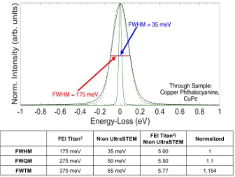
In Figure 1, the ZLPs collected through the CuPc specimen as well as a table comparing their
widths at FWHM, FWQM (full-width at quarter-maximum) and FWTM are shown. The energy
experiments as measured through the specimen) is better than on the Titan (best observed in our
microscope is 50 meV, 175 meV for the beam settings used for these experiments as measured
through the specimen) by a factor of five. This improvement in energy resolution makes it
realistic to observe peaks at energy-losses below 1eV.
In order to compare the shape of the ZLP on both instruments, the Nion ZLP was
numerically broadened to match the FWHM of the ZLP from the Titan (shown as the dashed
green line on Figure 1). There is very good agreement between the shapes of the ZLPs on the
two instruments. A small difference between this simulated ZLP and the ZLP from the Titan
instrument is observed as a 10% change at FWQM and 15% at FWTM (Figure 1). Although the
instruments have different monochromator designs Ð the Titan utilizes a Wien filter22 and the
Nion utilizes an alpha filter19 Ð it is not obvious that this would contribute to this observed
difference in zero-loss peak shape. The Titan data was recorded at a smaller dispersion (0.025
eV/channel) than on the Nion (0.005 eV/channel), but the EELS data collected on the Titan does
not become limited by the PSF unless the dispersion used is 0.325 eV/channel or less (see Figure
S1). Thus, the small difference in the two ZLPs could be due to differences in the higher-order
spectrometer aberrations as the Nion is fitted with a modified Gatan Enfinium spectrometer
Figure 1: Comparisons between the ZLPs collected on the Nion (solid green) and the Titan
(solid black). A theoretical ZLP with the same energy resolution as the Titanis shown for the
Nion (dashed green). Additionally, specific values of FWHM, FWQM, and FWTM are compiled
(see table).
The spectra collected prior to zero-loss subtraction from each microscope are shown in
Figure 2. It is apparent that some of the low energy spectral features are unambiguously
determined in the Nion data due to the reduced FWHM of the ZLP. For example, the features
indicated by red arrows (Figure 2) Ð in C60 at 2 eV; in PCBM at 2.5 eV; in P3HT at 2.6 eV Ð
appear as shoulders on the ZLP in the Titan data, whereas they are more clearly defined as
distinct peaks in the Nion data. In the CuPc data, the features in the range 6 Ð 8 eV, indicated by
the blue arrows (Figure 2), are also more defined in the Nion data.
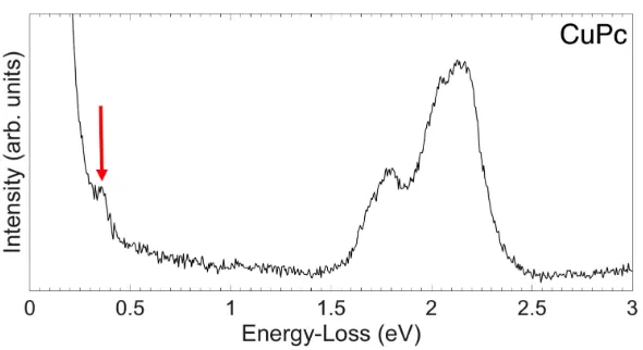
[image:9.612.151.487.75.328.2]peak can be identified in the data from both microscopes. The exception is the peak at ~360 meV
in the spectrum collected from CuPc on the Nion (Figure 3). This peak is present in the EEL
spectra collected from all four materials, although the center energy ranges from 250 meV to 400
meV. For the materials in which the peak is centered at about 400 meV, this low energy-loss
feature could be attributed to an O-H bond stretching mode,23 although it might also have
overlapping contributions from C-C and C-H vibrational modes, and it is these C-C and C-H
modes which are likely measured in the lower energy vibrational peaks. In summary, these
qualitative comparisons illustrate how the improved resolution of the Nion, as compared to that
of the Titan, makes it easier to definitively identify spectral features, especially weak peaks at
very low energy-losses.
The intensity of the inelastic signal in energy-loss spectroscopy is greatest in the
valence-loss region which means that valence-valence-loss spectroscopy has enormous potential for
beam-sensitive materials, such as those found in polymers, composites, biomaterials, and OPVs.
Furthermore, since the complex dielectric function can be extracted from the valence loss
spectrum, it is possible to obtain information about the optical and electronic properties of the
material with nanometer scale spatial resolution. We have reported previously on the use of this
technique to obtain the optical properties of OPV materials.13 The next step in the comparison of
the Nion and Titan data is to compare the real and imaginary parts of the complex dielectric
function to determine the impact of the improved energy resolution of the Nion. There are three
steps to achieve this: (1) fitting and subtraction of the ZLP, (2) deconvolution to remove plural
scattering and obtain the single scattering distribution (SSD), and (3) Kramers-Kronig (KK)
analysis of the SSD to obtain the complex dielectric function. The deconvolution and KK
majority of the inelastic scattering and that allows the fitting of a function to extend the data to
high energy loss. As discussed below this creates significant challenges when the data are
[image:11.612.97.517.185.427.2]acquired with very high energy dispersion.
Figure 2: Comparison of energy-loss spectra collected on the Nion (green) and the Titan (black)
for (a) CuPc, (b) P3HT, (c) C60, and (d) PCBM.
The ZLP from the collected spectra was removed using the reflected tail method in GatanÕs
DigitalMicrograph software.24 In principle, the partial ZLP on the negative (energy-gain) side of
zero energy is ÒreflectedÓ onto the energy-loss side and fitted in a defined energy window and
spliced into the experimental spectrum. For the data collected on the Titan, this was
straightforward. The spectra were collected with an extended negative energy range (-10.0 eV) to
energy-loss side was adjusted to ensure that any artifacts at the splicing point did not coincide
with spectral regions of interest.
Figure 3: Nion CuPc spectrum displaying the peak attributed to an O-H bond stretch (at about
0.36 eV).
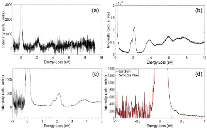
However, due to the high dispersion of the Nion data, the ZLP extraction process was less
straightforward for these spectra. Since the data were collected in dual-EELS mode, the splicing
tool in GatanÕs DigitalMicrograph software was used to merge together the full ZLP (Figure 4a)
with the low-loss (~0.05 to 10 eV) spectrum (Figure 4b). However, this made the reflected tail
method for ZLP extraction impossible due to the poor signal-to-noise ratio (SNR) on the energy
gain side of the ZLP (Figure 4c). This is a result of the short acquisition times used during the
data collection for spectra that included the ZLP. This poor SNR compromised the ZLP
extraction routine (Figure 4d), as the tail from the left side of the ZLP was not accurately
[image:12.612.159.454.152.313.2]Figure 4: The (a) ZLP and (b) high-resolution low-loss spectra collected in dual-EELS mode on
the Nion for CuPc. These two spectra were spliced together, which resulted in the spectrum in
(c). Due to the large noise signal on the left side of the ZLP in (c), the ZLP extraction routine did
not work properly (d).
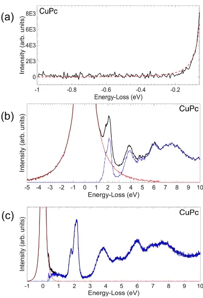
To overcome the issues in the Nion data, a modified Voight function was used to fit the
shape of the tail on the negative (energy-gain) side of the experimental ZLP:
� ∆� =
2�� 4 ln (2)� �01 23 4 ∗(∆6)7
�� (4(∆�)4+ �4)
where a, b, and c are fitting coefficients, and ΔE is the energy-gain. After fitting the tail, the
noisy data on the left side of the ZLP was replaced with the smoothed data from the fit. This fit
was conducted on the experimental ZLP data up to -0.06 eV, as this was the highest energy that
for CuPc. The region with poor SNR on the left side of the experimental ZLP was replaced with
the smoothed fit which then allowed removal of the ZLP from the experimental data using the
previously described reflected tail method. Figure 5 shows the successful ZLP extractions for the
CuPc EELS data collected on the (b) Titan and (c) Nion. In both spectra, the tails are accurately
reflected from the left side of the ZLP to the right. This process was repeated for all four
materials.
In order to perform the deconvolution step to remove plural scattering and obtain the single
scattering distribution (SSD), the energy-loss spectra need to extend to an energy-loss
significantly beyond that of the plasmon peak (the broad peak at ~20 to 30 eV associated with
collective oscillations of the valence electrons). This is necessary to meet the requirement that
the experimental spectrum falls almost to zero intensity at both ends of the energy-loss range to
avoid ÒringingÓ artefacts in the application of the discrete Fourier transform.14 This constraint is
easily met on the low (energy-gain) side of the ZLP. At finite energy-losses it is necessary to
numerically extrapolate the data to high energy-loss. This is straightforward if the experimental
spectrum has been recorded up to an energy-loss beyond that of all collective excitations so that
a smooth monotonic function can be fitted and extrapolated using routines in DigitalMicrograph.
This is the case for the Titan data as the low-loss spectra were recorded to approximately 40 eV
since the resolution was not point-spread limited in the conditions used i.e. DE=175 meV.
However, as mentioned in the methods section, to obtain the high-resolution (DE=35 meV) data
on the Nion, the low-loss spectra could only be collected to approximately 10 eV. Thus, it was
necessary to splice this spectrum with the lower resolution data recorded over an extended
energy range (-5 to 35 eV). Since these data were collected at a lower dispersion to
match the dispersion of the low-loss spectra. This interpolated extended energy-loss spectrum
was then spliced with the low-loss spectrum at approximately 10 eV. This resulted in a final
spectrum consisting of the high-resolution low-loss data from -1 to 10 eV and of the interpolated
extended low-loss data from 10 to 35 eV.
Figure 5: (a) Results of fitting the tails of the ZLP for the Nion CuPc data. As is shown, the
fitted function (red dashed line) models the experimental (black line) well. (b) Successful ZLP
extractions for data collected on the Titan and the (c) Nion for CuPc. The black, red, and blue
lines denote the raw data, zero-loss peak, and inelastic spectra, respectively.
The complex dielectric function, �(�), is a causal function25 that is related to the SSD, J1(E),
[image:15.612.200.410.206.513.2]�< � ∝ Im −1
�(�)
Thus, the SSD can be analyzed via a Kramers-Kronig transformation to determine Re [1/ε(E)]
from Im [1/ε(E)].25 The real and imaginary parts of the complex dielectric function (ε1 and ε2,
respectively) were calculated as:14
� � = �< � + ��4 � =
Re 1 � � + � Im −1 � �
Re 1 � � 4 + Im −1 � � 4
ε1 and ε2 were obtained from each of the EELS spectra collected using the Kramers-Kronig
analysis routine in DigitalMicrograph. Figures 6 and 7 shows these resulting real (ε1) and
imaginary (ε2) parts of the dielectric function, respectively, for each of the materials investigated.
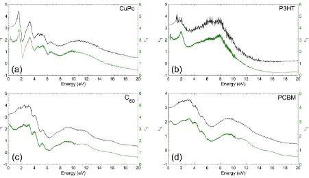
Figure 6: The ε1 spectra collected on the Nion (green) and the Titan (black) for (a) CuPc, (b)
P3HT, (c) C60, and (d) PCBM. Comparisons of these spectra show that no new peaks are
[image:16.612.82.533.345.606.2]
The ε1 plots are generally in good agreement for the two instruments, but the data collected
on the Nion is better resolved (Figure 6). For instance, in the CuPc ε1 plot from the Nion data,
there are two defined peaks at approximately 1.5 Ð 2.0 eV, whereas the second peak appeared to
be just a shoulder on the right of the primary peak in the Titan data set. A similar observation can
be made for the C60 ε1 data in which the two distinct peaks in the Nion spectrum at
approximately 2.75 eV appeared to be just one broad peak in the data collected on the Titan.
There is also better definition in the Nion ε1 spectra for PCBM (see the two peaks at
approximately 2.5 eV) and P3HT (see the peak at 2.0 eV).
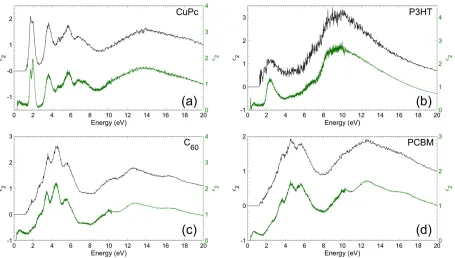
The imaginary, ε2, part of the dielectric function can be directly related to single electron
transitions between the valence and conduction bands in the material. These comparisons
between the ε2 spectra should highlight any new electronic information obtained as a result of the
improved energy resolution of the Nion. Again, measurements on the Nion resulted in slightly
better resolved peaks (Figure 7). However, in the CuPc ε2 spectrum collected on the Nion, the
relative intensities of the two peaks at approximately 2.0 eV are reversed. The relative intensities
in the Nion data are in good agreement with optical ellipsometry data available in the literature.26
It is probable that the reversal in peak intensities in the Titan data is due to errors in the ZLP
extraction. It is possible that all of the intensity due to the ZLPÕs tail was not actually removed
from the spectrum, which would have resulted in excess intensity in the low energy range of the
inelastic spectrum. However, for all four materials there are no new peaks observed in any of the
ε2 plots and the assignment of features to single electron transitions is unchanged from an earlier
analysis.13 This would be expected, as the native line widths of the features in the low-loss
monochromating the electron beam is that more separation is observed between closely spaced
features in the spectra. While, at least for these OPV materials, there is little advantage to
collecting data on the Nion other than simplifying the data analysis, comparisons between the
Nion and Titan data sets exemplify how the monochromator is critical for observing features that
are closely spaced together.
Figure 7: The ε2 spectra collected on the Nion (green) and the Titan (black) for (a) CuPc, (b)
P3HT, (c) C60, and (d) PCBM. Comparisons of these spectra show that no new peaks are
observable in the Nion data.
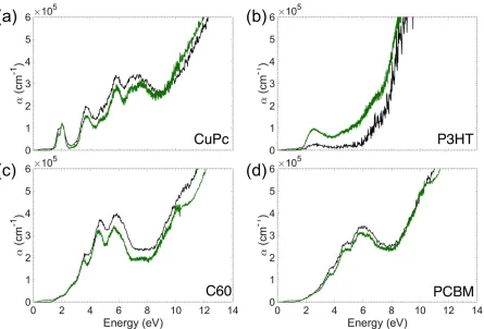
To be more quantitative in the comparison between the Titan and Nion data sets, the
absorption coefficient, α, was extracted from the EELS data for all four materials. The absorption
coefficient is related to the extinction coefficient, κ, as α = 4πκ/λ where λ is the wavelength.
Furthermore, κ is related to ε1 and ε2 as ε1 = n2-κ2 and ε2= 2nκ where n is the refractive index. It
[image:18.612.80.535.209.467.2]absorption coefficient as a function of energy-loss for both the Titan and Nion data for all four
materials. There is extremely good agreement between these data sets. Additionally, the
inversion of the relative intensities of the first two peaks in the CuPc is no longer observed,
which can be attributed to the fact that α depends not only on ε2, but also on ε1.
Overall, these plots show that monochromated STEM-EELS is a very powerful approach to
making spatially resolved measurements of the absorption coefficient, even in beam sensitive
organic materials.
Figure 8: The α spectra determined from EELS data collected on the Nion UltraSTEM (green)
and the FEI Titan3 (black) for (a) CuPc, (b) P3HT, (c) C60, and (d) PCBM.
[image:19.612.81.526.291.593.2]In this work, EELS spectra were collected on two monochromated scanning transmission
electron microscopes with differing energy resolution capabilities for CuPc, C60, P3HT, and
PCBM. The superior energy resolution of the Nion UltraSTEM 100 MC ÔHERMESÕ microscope
(35 meV energy resolution in the beam conditions used here) improved the resolution of the
peaks in the raw spectra and made it possible to measure spectral features below 2 eV, including
an O-H bond stretch at approximately 0.4 eV. However, for the materials being investigated no
new peaks were measured in the imaginary part of the complex dielectric function, indicating
that, for these specific materials, the data collected on an FEI Titan3 60-300 Image-Corrected
S/TEM (175 meV energy resolution in the beam conditions used here) can be processed to obtain
the same electronic information as for data collected on the Nion. We have demonstrated how
monochromated STEM-EELS data can be manipulated to extract the absorption coefficient. It is
concluded that monochromated STEM-EELS in the valence loss region shows great promise for
determining optical properties with high spatial resolution even in beam sensitive materials.
Acknowledgements
This paper is dedicated to Dr. Ondrej Krivanek. His work on electron spectrometers and electron
monochromators has had a major influence on the use of electron energy-loss spectroscopy in the
microscopy community and has opened many opportunities for investigation of new materials
and phenomena. The authors would like to thank all collaborators and technical support at both
the Center for Electron Microscopy (CEMAS) at The Ohio State University and the Materials
and Manufacturing Directorate at the Air Force Research Laboratory (AFRL) at
Wright-Patterson Air Force Base. Funding was provided by an AFRL/DAGSI Ohio-Student Faculty
Directorate, and by The Ohio State University through a Distinguished University Fellowship.
The SuperSTEM Laboratory is the U.K. National Facility for Aberration-Corrected Scanning
Transmission Electron Microscopy, supported by the Engineering and Physical Sciences
Research Council (EPSRC).
References
1. C.J. Brabec, A. Cravino, D. Meisser, N.S. Sariciftci, T. Fromherz, M.T. Rispens, L. Sanchez &
J.C. Hummelen. Origin of the open circuit voltage of plastic solar cells. Adv. Funct. Mater. 11,
374-380 (2001).
2. R.F. Service. Outlook brightens for plastic solar cells. Science 332, 293 (2011).
3. D. Chen, A. Nakahara, D. Wei, D. Nordlund & T.P. Russell. P3HT/PCBM bulk heterojunction
organic photovoltaic: correlating efficiency and morphology. Nano Lett. 11, 561-567 (2011).
4. M. Pfannmšller, H. Flugge, G. Benner, I. Wacker, C. Sommer, M. Hanselmann, S. Schmale,
H.Schmidt, F.A. Hamprecht, T. Rabe, W. Kowalsky & R.R. Schroder. Visualizing a
homogeneous blend in bulk:heterojunction polymer solar cells by analytical electron microscopy.
Nano Lett. 11, 3099-3107 (2011).
5. M. Pfannmšller, H. Flugge, G. Benner, I. Wacker, W. Kowalsky & R.R. Schroder. Visualizing
photovoltaic nanostructures with high-resolution analytical electron microscopy reveals material
phases in bulk heterojunctions. Synth. Met.161, 2526-2533 (2012).
6. L.F. Drummy, R.J. Davis, D.L. Moore, M. Durstock, R.A. Vaia & J.W.P. Hsu. Molecular-scale
and nanoscale morphology of P3HT:PCBM bulk heterojunctions: energy-filtered TEM and
7. SS. van Bavel, M. Barenklau, G. de With, H.Hoppe & J. Loos. P3HT/PCBM bulk heterojunction
solar cells: impact of blend composition and 3D morphology on device performance. Adv. Funct.
Mater. 20, 1458-1463 (2010).
8. B.V. Andersson, S. Masich, N. Solin & O. InganŠs. Morphology of organic electronic materials
imaged via electron tomography. J. Microsc. 247, 277-287 (2012).
9. B.V. Andersson, A. Herland, S. Masich & O. InganŠs. Imaging of the 3D nanostructure of a
polymer solar cell by electron tomography. Nano Lett. 9, 853-855 (2009).
10. S. van Bavel, E. Sourty, G. de With, K. Frolic & J. Loos. Relation between photoactive layer
thickness, 3D morphology, and device performance in P3HT/PCBM bulk-heterojunction solar
cells. Macromolecules 42, 7396-7403 (2009).
11. S.S. van Bavel, E. Sourty, G. de With & J. Loos. Three-dimensional nanoscale organization of
bulk heterojunction polymer solar cells. Nano Lett. 9, 507-513 (2009).
12. J.B. Gilchrist, T.H. Basey-Fisher, S.C. Chang, F. Scheltens, D.W. McComb & S. Heutz.
Uncovering the buried interface in organic solar cells. Adv. Funct. Mater. 24, 6473-6483 (2014).
13. J.A. Alexander, F.J. Scheltens, L.F. Drummy, M.F. Durstock, J.B. Gilchrist, S. Heutz & D.W.
McComb. Measurement of optical properties in organic photovoltaic materials using
monochromated electron energy-loss spectroscopy. J. Mater. Chem. A 4, 13636-13645 (2016).
14. R.F. Egerton. Electron Energy-Loss Spectroscopy in the Electron Microscope. (Springer, 2011).
15. R.F. Egerton. New techniques in electron energy-loss spectroscopy and energy-filtered imaging.
Micron 34, 127-139 (2003).
16. R.F. Egerton. Limits to the spatial, energy and momentum resolution of electron energy-loss
17. A.M. Lesk. Introduction to Symmetry and Group Theory for Chemists. (Kluwer Academic
Publishers, 2004).
18. O.L. Krivanek, T.C. Lovejoy, N. Dellby, T. Aoki, R.W. Carpenter, P. Rez, E. Soignard, J. Zhu,
P.E. Batson, M.J. Lagos, R.F. Egerton & P.A. Crozier. Vibrational spectroscopy in the electron
microscope. Nature 514, 209-212 (2014).
19. O.L Krivanek, J.P. Ursin, N.J. Bacon, G.J. Corbin, N. Dellby, P. Hrncirik, M.F. Murfitt, C.S.
Own & Z.S. Szilagyi. High-energy-resolution monochromator for aberration-corrected scanning
transmission electron microscopy/electron energy-loss spectroscopy. Phil. Trans. R. Soc. A. 367,
3683-3697 (2009).
20. O.L. Krivanek, T.C. Lovejoy, N. Dellby, & R.W. Carpenter. Monochromated STEM with a 30
meV-wide, atom-sized electron probe. Microscopy 62, 3-21 (2013).
21. O.L. Krivanek, T.C. Lovejoy, M.F. Murfitt, G. Skone, P.E. Batson & N. Dellby. Towards sub-10
meV energy resolution STEM-EELS. J. of Phys.: Conference Series 522, 012023 (2014).
22. P.C. Tiemeijer. Operation modes of a TEM monochromator. Proc. EMAG Õ99, Sheffield.
Institute of Physics Conference Series, no. 161, pp. 191-194. Bristol, UK: Institute of Physics
(1999).
23. D.M. Carey & G.M. Korenowski. Measurement of the Raman spectrum of liquid water. J. Chem.
Phys. 108, 2669-2675 (1998).
24. DigitalMicrograph EELS Analysis UserÕs Guide. (2003).
25. D.W. Johnson. A Fourier series method for numerical Kramers-Kronig analysis. J. Phys. A Math.
Gen. 8, 490Ð496 (1975).
26. D. Datta, V. Tripathi, P. Gogoi, S. Banerjee & S. Kumar. Ellipsometric studies on thin film