© 2015, IRJET.NET- All Rights Reserved Page 19
Two stage Cascade BJT Amplifier
N K Kaphungkui
Assistant professor, Electronics & Communication Department, Dibrugarh University, Assam, India
---***---Abstract
- Two stage BJT amplifiers for very small signal amplification is presented in this work. With maximum 20V supply voltage and 6mV peak to peak input signal, a fraction of input signal 130uV goes to the first pre amplifier stage and produces an output signal of 11.25V peak to peak at the second stage. The overall gain of the circuit is 86538 times the small signal appearing across the input terminal of the first stage. The design circuit works best for input voltage swing from 100uV peak to peak till 6 mv peak to peak signal voltage. The variation of amplifier gain wrt Vcc is also analyzed. From 7V till 20V if Vcc is varied the gain linearly increases. Maximum gain of 65.24db without output distortion is obtained when the supply voltage is 20V with the least bandwidth. Minimum gain of 31db is obtained with the least 7V voltage supply but having the highest bandwidth. The output noise voltage is from 1.6uV/Hz1/2 till270uV/Hz1/2 as supply voltage increases. The main objective
of this work is to optimized and enhanced both gain and bandwidth of the amplifier for very small and low frequency signal amplification.
Key Words:
emitter follower, voltage divider bias,
bypass capacitor, input voltage swing, bandwidth.
I.INTRODUCTION
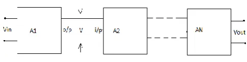
A single stage amplifier didn’t provide sufficient gain and bandwidth and moreover didn’t have matched input and output impedance. To overcome such problems multiple amplifiers are combined for better performance and amplification. Multiple amplifiers are connected in cascade to increase the overall voltage gain of the amplifier. In this type of configuration the output of one amplifier is the input of the next stage as shown in Fig.1. With this arrangement the gain of the amplifier can be increase tremendously [5], [6]. When n numbers of amplifier stages are connected in succession it is called multistage or researches with different approaches. To increase the overall gain, hybrid combination of BJT-FET-BJT in Triple
Darlington topology has already proposed and
successfully implemented as high power gain small-signal amplifiers in audio-frequency-range [1]. Two identical JFET in Darlington pair for small signal amplification with wide bandwidth is also carried out. Here variation of gain
wrt frequency, biasing resistance, temperature
dependency is also presented [2]. Design of high frequency low noise amplifier for wireless communication is also design. BJT is used as LNA to amplify the received RF path with high gain and high sensitivity [3]. Multistage BJT differential power amplifier delivering a power gain of 6db with high efficiency and linearity is also presented [4]. This work is carried on cascade amplifier with two stages having an overall gain of A1*A2 for very small signal amplification in audio frequency range. Between the two stage emitter follower is inserted for impedance matching to deliver maximum power to the preceding stage. Both the two stages are biased in the active mid- point operating region for maximum output swing without distortion [5]. Both AC and DC analysis of the amplifier is also presented. All important parameters of amplifiers like operating point, AC analysis, transient analysis, DC sweep and output noise analysis is also analysed.
CIRCUIT IMPLEMENTATION AND SIMULATION RESULT
© 2015, IRJET.NET- All Rights Reserved Page 20 the output of the amplifier without distortion. As the input
is dividing between the high series input resistance and low internal input impedance of the amplifier only a fraction of input will be amplified initially by the first stage which is built around Q1. Finally the output from the first stage is amplified by the second stage Q2. The emitter follower is inserted in this circuit for impedance matching between the two stages as shown in Fig.2.
Fig. 2 Two-stage small signal amplifier
DC analysis: The DC equivalent circuit of the amplifier stage is obtained by opening all capacitor and shorting all input source as shown in Fig.3. The transistor follows voltage divider biasing method [5]. Biasing resistances are designed to make the transistor operate in the active region. All the calculated values of the operating point of the transistor along with the simulation results are shown in Fig. 4.
Fig.3 DC equivalent circuit
Calculated DC operating values
Simulation results
ICQ = 1.66mA ICQ = 1.74mA
Vce = 10.04 V Vce =9.59V
Vbb = 2.36V Vbb =2.34V
Vc = 11.7V Vc = 11.27v
Ve= 1.66V Ve=1.68V
Fig. 4 comparison of results
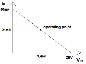
Fig 5. DC load line and operating point of Q1
The transistor is biased in the active region for maximum gain undistorted output as shown in the DC load line in Fig. 5. The
current gain β of the device is 337. The output of the first stage is
directly coupled to the emitter follower eliminating the need of biasing resistor for the emitter follower. The collector voltage of Q1 is used to bias the emitter follower which has a gain slightly less than 1. The operating point of emitter follower is shown in Fig.6.
© 2015, IRJET.NET- All Rights Reserved Page 21
AC Analysis: AC equivalent circuit is obtained by shorting all capacitor and grounding the DC supply voltage and replacing the transistor with T model as shown in Fig. 7
Fig.7 AC equivalent circuit
The gain of the amplifier is the ratio of output to input
A
v= (o/p vol)/(i/p vol)
(2)o/p vol is the total output voltage seen across Rc and the i/p vol
is the voltage seen across the base emitter resistor re having a
magnitude of 25mV/Ic. Therefore the gain of the amplifier can be
express as
A
v=( -5k* I
c)/(r
e*I
e)
A
v= -5k/r
esince I
c~ I
e (3)The input impedance Zi of the circuit is given by
Zi= Rp// (β+1)
r
e (4)And the amplifier output impedance Zo is express as
Z
o=R
c (5)Based on these three parameters i.e gain, input impedance and output impedance the overall amplifier circuit representation is shown in Fig.8
Fig. 8 General amplifier equivalent circuit
The negative sign in the gain expression indicates the input and output are out of phase by 180o. The gain in db and bandwidth of
the amplifier as a function of supply voltage with 6mv peak to peak input signal is shown in Fig. 9
Supply voltage Vcc
Gain in db bandwidth
7v 31db 5hz-1.5Mhz
9v 43.30db 7hz-1Mhz
11v 50.20db 10hz-750Khz
13v 55.06db 13hz-614Khz
15v 58.93db 17hz-503Khz
17v 61.75db 19hz-447Khz
19v 64.23 21hz-450Khz
20v 65.24db 23hz-400Khz
Fig.9 variation of gain and BW wrt Vcc
The circuit work best from 7V to 20V Vcc. Gain of the amplifier as a function of Vcc is shown on Fig.10.
Fig.10 Graphical interpretation of Vcc Vs gain
© 2015, IRJET.NET- All Rights Reserved Page 22
The amplifier circuit consists of three 2N30904 transistor as shown in Fig.1. The first and the last stage follow the same biasing technique i.e voltage divider and in between the two stages, emitter follower is inserted to provide a good overall voltage gain and for proper impedance matching between the two stages. This reduces the attenuation due to inter-stage loading. Both the stages i.e first stage and the output stage is bias in the active region for maximum signal swing without clipping. Full amplification is obtained in the second stage which swings around ground reference voltage. Circuit elements for the propose amplifier is listed below in the component table.
List of components
components quantity
2N3904 transistor 3
500 uF bypass capacitor 1
500 uF bypass capacitor 1
100uF coupling capacitor 1
10uF coupling capacitor 2
9KΩ resistor 2
500Ω 1
5 kΩ resistor 2
1k Ω 4
33KΩ 1
Fig.11 circuit component list
The AC simulation is carried out with input voltage of 6mV p-p and supply voltage of 20V. It has a constant gain of 65.24db within the bandwidth and after 400 KHz it roll off as shown in the simulation result in Fig. 12
Fig.12 AC signal simulation result
With the same input condition and supply voltage, transient analysis and output noise analysis is carried out as shown in Fig 13 & 14. From the
simulation result the amplified output voltage swing is 11.25V peak to peak and the noise is 270uV/Hz1/2.
Fig.13 transient analysis of output
Fig.14. output noise analysis
The effect of DC sweep supply voltage wrt ICQ and IEQ is also
analyzed as shown in Fig.15. Both the operating current which is almost equal linearly rises from 0.2mA to 1.74mA from the simulation result
Fig.15 DC sweep simulation result
3. CONCLUSIONS
© 2015, IRJET.NET- All Rights Reserved Page 23
REFERENCES
[1] SachchidaNand Shukla and Susmrita Srivastava “A Novel Circuit Model of Small-Signal Amplifier Developed by Using BJT-JFET-BJT in Triple Darlington Configuration” International Journal of Advanced Research in Electrical, Electronics and Instrumentation Engineering Vol. 1, Issue 5, November 2012
[2] Dr. SachchidaNand Shukla, Susmrita Srivastava “A New Circuit Model of Small-Signal Amplifier using JFETs in Darlington pair Configuration” International Journal of Advanced Research in Electrical, Electronics and Instrumentation Engineering Vol. 2, Issue 4, April 2013
[3] Oluwajobi F. I, Lawalwasiu “MULTISIM DESIGN AN SIMULATION OF 2.2GHz LNA FOR WIRELESS COMMUNICATION” International Journal of VLSI design & Communication Systems (VLSICS) Vol.5, No.4, August 2014.
[4] Rajesh Kumar, Dr. O. P. Singh “A HIGH GAIN AND EFFICIENT MULTISTAGE BJT DIFFERENTIAL POWER AMPLIFIER” International Journal of Emerging Technologies in Computational
and Applied Sciences (IJETCAS) pg- 596-598.
[5] David A. Bell, Electronic devices and circuits, V Edition., Oxford University Press India, 2008, Pg. 166-169, 196-202, Pg. 246-253.
[6] Donald A Neamen, electronics circuit, 3rd Edition, Tata McGraw Hill, 2007, Pg. 303-326 .Pg. 399-424.
[7] R. L. Boylestad and L. Nashelsky, Electronic Devices and Circuit Theory, Pearson Education Asia, 3rd ed., Pg.263,307,600, 2002
[8] Thomas L. Floyd, Electronic devices, Pertice Hall, 4th edition Pg. 46-60.
BIOGRAPHIES
N. K. Kaphungkui
Completed Diploma in Electronics Engineering in the year 2004 from DOEACC centre and after that received B.Tech. Degree in Electronics and Communication in the year 2007 from North East Regional Institute of Science and
Technology. And after that
pursue M.Tech in Electronics Design and Technology in 2009 and completed in the year 2011 from Tezpur University. Presently working as faculty member in Electronics and Communication
Department, Dibrugarh
University, Assam, India. Area of research interest includes VLSI circuit design, low power CMOS circuit design. simulation of circuit and implementing with hardware