Abstract
Schrader, Michael John. Considerations for Electrical Characterization of MOS
Capacitors that Arise Due to Processing. (Under the direction of Richard T. Kuehn)
The goal of this research was to determine the effects that the actual physical
structure of an overlapped metal-oxide-semiconducter (MOS) capacitor and an etch bias have
on the extraction of the gate-oxide thickness. Included in these concerns were the overlap of
the field oxide by the gate electrode, the angle of the active-area sidewall, and the increase in
size of the active area due to an etch bias. In addition, the growth of a contaminant layer, or
ad-layer, on oxides that do not have a permanent gate-electrode was addressed. This ad-layer
forms immediately after a wafer is exposed to the lab ambient and causes a significant
increase (i.e., ~ 10%) in the apparent thickness of the oxide.
The refinement of the total capacitance to the active-area capacitance uses measured
data from Hg-gated capacitors on p-type Si wafers and Al / Poly-Si gated capacitors on both
p- and n-type Si wafers. The effects of a non-vertical sidewall and an etch bias are addressed
theoretically through the use of the classic treatment of capacitance.
The capacitance-voltage characteristics from the MOS capacitors were used to extract
the oxide thickness (tox). The extracted thickness was determined from a model-based
methodology (i.e., the slope method) and a model-based analysis (i.e., NCSU’s CVC model).
model-based analysis of the active-area capacitance characteristics results in a consistent
oxide thickness over the range of capacitor areas that were available.
The removal and re-growth of the ad-layer were investigated using current-voltage
and capacitance-voltage characteristics from blanket oxides on both p- and n-type silicon
wafers. The changes in these characteristics were quantified as the ad-layer grows over time.
The C-V characteristics were analyzed using NCSU’s CVC program in order to extract
values for oxide thickness, flatband voltage, and interface trap densities. The ad-layer causes
considerable inaccuracies in the model extraction of oxide thickness as well as the flatband
voltage and interface trap density. Electrical and optical results on the p-type wafer both
show that the ad-layer increases the apparent oxide thickness by ~ 0.25 nm and the electrical
Considerations for Electrical Characterization of MOS Capacitors
that Arise Due to Processing
by
Michael John Schrader
A thesis submitted to the Graduate Faculty of North Carolina State University
In partial fulfillment of the Requirements for the Degree of
Master of Science
Electrical Engineering
Raleigh
2001
APPROVED BY:
Dedication
Biography
Michael Schrader was born and raised in Raleigh, NC. As a youngster he was involved in
several sports including soccer, basketball, and football. At an early age he was determined
to attend UNC-Chapel Hill, but after growing up decided that NCSU would be far superior.
After receiving his BS in Materials Science and Engineering at NCSU he decided to continue
his education with an MS in Electrical Engineering from NCSU since he had become
fascinated with MOSCaps and MOSFETs as an undergrad.
During his education he met many fun and interesting people. Early in his undergraduate
education Michael met two professors that made a huge impact on his life, Drs. Dennis
Maher and Richard Kuehn. These two teachers/advisors were always willing to help and
point him in the right direction (no matter how bad he screwed up). Fellow students also had
an impact on Michael. The first graduate student he worked with, Joe Clark, helped fan the
flame of interest, Brian “Big Nasty” Harding added more fuel to the fire, Shweta “Little
Brown Girl” Shah was the friendly contender for the best grades, Rob Trussell was the social
event manager that prevented Michael from losing his mind, Andy (oberho) Oberhofer
provided a never-ending conversation about Nintendo and Sony Playstation, Kwangok
“koh-man” Koh showed him improved measurement and organizational techniques, and Chad
Acknowledgements
I would like to thank my committee members Drs. Richard Kuehn, Dennis Maher, and Veena
Misra for their patience and insight. Shweta Shah for the processing and electrical testing
she contributed. Kwangkok Koh and Chad Young for the creation of the ‘tox Tables’. Steven
Table Of Contents
LIST OF TABLES……….vii
LIST OF FIGURES………...….ix
CHAPTER 1 INTRODUCTION………1
CHAPTER 2 BACKGROUND………..……….3
2.1 Band Diagrams for a MOS Capacitor………..………...3
2.2 The Components of a MOS Capacitor………5
2.2.1 Substrate………5
2.2.2 Gate Dielectric………...6
2.2.3 Gate Electrode………...7
CHAPTER 3 WAFER PROCESSING………12
CHAPTER 4 THE EXTRACTION OF A STATISTICALLY-ROBUST ACTIVE AREA OXIDE THICKNESS FROM OVERLAPPED MOS CAPACITORS………...…16
4.1 Introduction………..……….16
4.2 Gate Electrode Overlap………..………...17
4.1.1 Hg-Caps………..……….19
4.1.2 Poly-Caps………..……….………..21
4.3 Sidewall Contributions………..………25
4.4 Etch Bias………...28
5.3 CVC Analysis Trends………..……….56
5.4 Correlation with Optical Trends………..……….58
CHAPTER 6 CONCLUSIONS……….72
LIST OF REFERENCES………..………75
APPENDICES……….…...77
APPENDIX A tox Look-up Tables………....78
APPENDIX B Round Robin………...92
APPENDIX C Current-Voltage Characteristics………..141
APPENDIX D Electrical Characteristics of Scaled Oxides Tables……….151
List of Tables
Table 2-1 Properties of silicon dioxide………..…6
Table 4-1 Gate electrode areas……….19
Table 4-2 CVC extracted tEOT from Hg-Caps characteristics………..20
Table 4-3 CVC extracted tEOT from n+/p Poly-Caps characteristics………....21
Table 4-4 CVC extracted tEOT from n+/n Poly-Caps characteristics………22
Table 4-5 Analysis methodology and extracted metrics………..23
Table 4-6 Flatband voltage from measured (CTOT) and corrected (Cox) C-V characteristics………...24
Table 4-7 Capacitance difference of vertical to non-vertical sidewalls………...28
Table 5-1 Trends in the modeled C-V characteristics for the p-type Blanket Wafer…...56
Table 5-2 Trends in the modeled C-V characteristics for the n-type Blanket Wafer…...57
Table A-1 Tabulated values of capacitance per unit area versus toxcorrected for NCSU's CVC model and a metal (Hg) / p capacitor………..80
Table A-2 Tabulated values of model-based capacitance per unit area (µF/cm2) versus toxcorrected for five models and a n+ poly-gate p substrate capacitor………..…82
Table A-3 Tabulated values of capacitance per unit area versus toxcorrected for NCSU's CVC model and an n+-gate on n substrate capacitor………...88
Table B-1 Parameter space of settings for HP 4284A LCR meter………...93
Table C-1 Flatband voltages of selected capacitors………143
Table C-2 Jave, Io, Ao, and R2 metrics extracted from current versus area plots……….143
Table C-3 Comparison of ∆tox from I-V and C-V of n+/p and n+/n wafers………144
Table D-3 Metrics extracted from n+/n overlapped capacitors with nominal oxide thickness of 1.5 nm………153
Table D-4 Metrics extracted from n+/n overlapped capacitors with nominal oxide thickness of 1.8, 2.1, and 2.4 nm………...…154
Table D-5 CVC extracted metrics from overlapped n+/p capacitor with nominal gate oxide thickness of 1.5 nm………..…154
Table D-6 CVC extracted metrics from overlapped n+/p capacitor with nominal gate oxide thickness of 1.8 nm………..155
Table D-7 CVC extracted metrics from overlapped n+/p capacitor with nominal gate oxide thickness of 2.1 nm………..155
Table D-8 CVC extracted metrics from overlapped n+/p capacitor with nominal gate oxide thickness of 2.4 nm………..…155
Table D-9 CVC extracted metrics from overlapped n+/n capacitor with nominal gate oxide thickness of 1.5 nm………..156
Table D-10 CVC extracted metrics from overlapped n+/n capacitor with nominal gate oxide thickness of 1.8 nm………..156
Table D-11 CVC extracted metrics from overlapped n+/n capacitor with nominal gate oxide thickness of 2.1 nm………..157
List of Figures
Figure 2-1 Wafer sized diagram of an Hg-Caps wafer showing the locations of capacitors of each area. Also shown is the L-strip, which has an oxide of the same thickness as the capacitors.
Figure 2-2 Expanding views of an Hg-Caps wafer from quadrant to array to device.
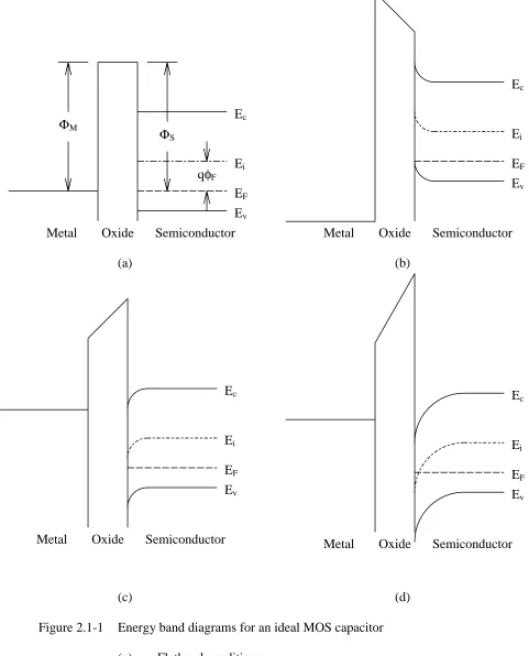
Figure 3.1-1 Energy band diagrams for an ideal MOS capacitor
(a) Flatband conditions (b) Accumulation (c) Depletion (d) Inversion
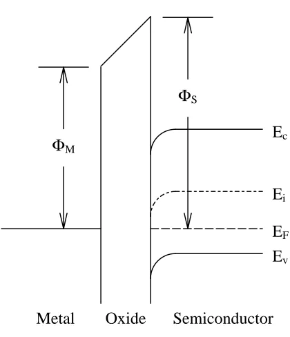
Figure 3.1-2 Energy band diagram for a non-ideal MOS capacitor. The metal-semiconductor workfunction difference is relatively small.
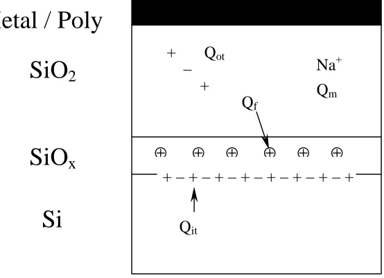
Figure 3.2.2 Locations of various charges within the oxide of an MOS capacitor i) Oxide trapped charge, Qot, is located in the oxide
ii) Mobile charge, Qm, due to contaminants
iii) Fixed charge, Qf, in the SiOx layer
iv) Interface trapped charge, Qit, at the interface between the oxide and the
substrate
Figure 4.1-1 Schematic drawings of MOS capacitor
(a) Typical parallel plate model
(b) Model incorporating the gate electrode overlap and non-vertical sidewalls
Figure 4.2.1-1 Plot of measured and modeled oxide capacitance versus voltage as a function of area for the average values of 10-20 Hg-Caps. There is excellent agreement in the accumulation region.
Figure 4.2.1-2 Total capacitance at – 2.5 V versus mask defined area for Hg-Caps. The slope of the linear fit corresponds to an oxide thickness of 2.6 nm and the intercept shows a field oxide contribution of ~ 31 pF.
nm. The intercept shows the capacitance for a zero area device to be 0.15 pF.
Figure 4.2.1-5 Modeled oxide capacitance at – 2.5 V versus mask defined active area for Hg-Caps. The slope gives an oxide thickness of 2.58 nm, which agrees with Figs. 4.1.1-2 and 4.1.1-4, and the intercept shows a capacitance of ~ 4 fF at zero area.
Figure 4.2.2-1 Plot of the C-V characteristics as measured and the corresponding model curves for n+/p Poly-Caps. There is good agreement in the accumulation and depletion regions.
Figure 4.2.2-2 Plot of the measured total capacitance at – 2.5 V versus area for the average values of 10-20 n+/p Poly-Caps. The slope of the linear fit gives toxcorrected =
2.36 nm and the intercept shows a field oxide contribution of ~ 4 pF.
Figure 4.2.2-3 Plot of the corrected and modeled oxide capacitance versus voltage as a function of area for the average values of 10-20 n+/p Poly-Caps. There is excellent agreement between the measured and modeled characteristics.
Figure 4.2.2-4 Plot of the measured oxide capacitance at – 2.5 V versus area for the average values of 10-20 n+/p Poly-Caps. The slope of the linear fit corresponds to toxcorrected = 2.34 nm.
Figure 4.2.2-5 Plot of the modeled oxide capacitance at – 2.5 V versus area. Model calculations were performed on the average oxide capacitance from 10-20 n+/p Poly-Caps. The slope of the linear fit gives toxcorrected = 2.33 nm, which
is in good agreement with the values from Figs. 4.1.2-2 and 4.1.2-4, and an intercept showing a capacitance at zero area of ~ 36 fF.
Figure 4.2.2-6 Plot of the C-V characteristics as measured and the corresponding model curves for n+/p Poly-Caps. There is good agreement throughout the voltage range.
Figure 4.2.2-7 Plot of the measured total capacitance at – 2.5 V versus area for the average values of 10-20 n+/n Poly-Caps. The slope of the linear fit gives toxcorrected =
2.41 nm and the intercept shows a field oxide contribution of ~ 4 pF.
Figure 4.2.2-8 Plot of the measured and modeled oxide capacitance versus voltage as a function of area for the average values of 10-20 n+/n Poly-Caps. There is excellent agreement between the measured and modeled characteristics.
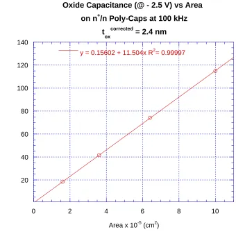
Figure 4.2.2-10 Plot of the modeled oxide capacitance at – 2.5 V versus area. Model calculations were performed on the average oxide capacitance from 10-20 n+/n Poly-Caps. The slope of the linear fit gives toxcorrected = 2.4 nm, which is
in good agreement with the value from Fig. 4.1.2-7, and an intercept showing a negative capacitance at zero area of ~ 65 fF.
Figure 4.3-1 Schematic of a MOS capacitor model used for sidewall capacitance calculations
(a) Cross-sectional view (b) Plane view
Figure 4.3-2 Diagram of wedge and column structures used for sidewall capacitance calculations
Figure 4.3-3 Plot of calculated sidewall capacitance versus area as a function of sidewall angle. The largest value is from a 45° sidewall for a 10.0 x 10⁻⁵ cm2 capacitor. Notice the value is only ~ 34 fF which is well below the sensitivity of NCSU measurement tools.
Figure 4.3-4 Plot of the calculated total capacitance versus area as a function of sidewall angle. The slopes of both linear-fits are identical and correspond to toxcorrected
of 2.01 nm, which compares favorably with the 2.0 nm value used for the calculation. The intercepts show CFox values that differ by 2 fF.
Figure 4.3-5 Plot of the absolute difference in calculated sidewall capacitance of the 45°and 90° models versus area. This shows that for small area capacitors the assumption of vertical sidewalls is valid since the error will be in the tens of fF range for a 10.0 x 10⁻⁵ cm2 capacitor.
Figure 4.4-1 Plot of the calculated total capacitance versus Area as a function of etch bias. All three curves lie practically on top of one another. The slopes of the linear-fit are nearly the same and give toxcorrected values that differ by 0.01
nm. The intercepts, giving CFox, differ by ~ 0.2 pF.
Figure 4.4-2 Plot of calculated oxide capacitance versus area as a function of etch bias. The slopes of the linear-fit are very close to each other and result in toxcorrected
differences of only 0.01 nm. The intercept for the curve without etch bias shows a Cox value at zero area of 0.149 pF.
Figure 5.2-2 Same as Fig. 5.2-1 except with additional curves at times of 6 and 24 hours and a reduced voltage range of – 0.5 to – 2.5 V. Notice the current is reduced with time, showing the re-growth of the ad-layer. Also the I-V characteristics measured after 48 hours are very nearly the same as that from the pre-bake measurement.
Figure 5.2-3 C-V characteristics from a p-type blanket wafer before a bake cycle of 200° C/60 sec, and at times of ~ 0 and 48 hours after the bake. After the bake Cmax
has increased by an amount equivalent to a ~ 0.2 nm decrease in oxide thickness. After the 48 hours Cmax is actually lower than its pre-bake value
suggesting an ad-layer thicker than that present before the bake.
Figure 5.2-4 Same as Fig. 5.2-3 except with a reduced voltage range of – 1.4 to – 0.2 V and additional curves at times of 6 and 24 hours. Notice the negative flatband shift of ~ 195 mV immediately after the 200° C/60 sec bake, and its return towards the pre-bake value over the 48 hour period. The flatband shift is thought to be the result of a positive charge that remains on the oxide after the desorption of the ad-layer. The ad-layer passivates the positive charge as it re-grows.
Figure 5.2-5 I-V characteristics from an n-type blanket wafer showing curves for before a 200°C/60 sec bake and times ~ 0 and 24 hours after the bake. Immediately after the bake the current at VFB + 1 V has increased by approximately one
decade which corresponds to a decrease in oxide thickness of ~ 0.2 nm.
Figure 5.2-6 Same as Fig. 5.2-5 except with additional curves at times of 6 and 17 hours and a reduced voltage range of – 0.5 to – 2.5 V. Notice the current is reduced with time, showing the re-growth of the ad-layer. Also the I-V characteristics measured after 24 hours are very nearly the same as that from the pre-bake measurement.
Figure 5.2-7 C-V characteristics from a n-type blanket wafer showing curves before a bake cycle of 200° C/60 sec, and times of ~ 0 and 24 hours after the bake. The runaway in the accumulation capacitance is attributed to the poor quality of the low-temperature oxide. Even though, after the 24 hour period the C-V characteristics are approaching the reference state.
Figure 5.3-1 Plot of modeled C-V characteristics from the p-type Blanket Wafer. There is an increase in the accumulation capacitance immediately after the bake that corresponds to a decrease in effective oxide thickness of ~ 0.25 nm. After the 48 hour period the modeled C-V characteristics are close to those from the reference state.
Figure 5.3-2 Same as Fig. 5.3-1 with a reduced voltage range of –1.4 to –0.2 V. Notice the negative shift in flatband voltage of ~ 200 mV immediately after the bake. The flatband voltage can be seen to shift towards the reference value over the 48 hour period
Figure 5.3-3 Plot of modeled C-V characteristics from the n-type Blanket Wafer. The modeled curve immediately after the bake is not included due to an extremely poor fit. However, at 6 hours the accumulation capacitance is ~ 200 pF greater than the reference value corresponding to a decrease in effective oxide thickness of ~ 0.35 nm. After the 24 hour period the modeled C-V characteristics are approaching the reference state.
Figure 5.3-4 Same as Fig. 5.3-3 except with a reduced voltage range of –0.2 to 0.8 V. The flatband voltage approaches the reference value in the 24 hour period.
Figure 5.4-1 Plot of apparent oxide thickness versus time showing desorption of the ad-layer at t ~ 0 hrs and the subsequent re-accretion of the ad-ad-layer over a 24 hour period.
Figure B-1 Plot of capacitance versus voltage as a function of area from a Poly-Cap with a nominal gate oxide thickness of 4.0 nm. Measurements were made in the parallel mode at 10 kHz with no instrument correction.
Figure B-2 Plot of capacitance versus voltage as a function of area from a Poly-Cap with a nominal gate oxide thickness of 4.0 nm. Measurements were made in the parallel mode at 10 kHz with an open circuit correction.
Figure B-3 Plot of capacitance versus voltage as a function of area from a Poly-Cap with a nominal gate oxide thickness of 4.0 nm. Measurements were made in the parallel mode at 100 kHz with no instrument correction.
Figure B-4 Plot of capacitance versus voltage as a function of area from a Poly-Cap with a nominal gate oxide thickness of 4.0 nm. Measurements were made in the parallel mode at 100 kHz with an open circuit correction.
Figure B-6 Plot of capacitance versus voltage as a function of area from a Poly-Cap with a nominal gate oxide thickness of 4.0 nm. Measurements were made in the parallel mode at 1 MHz with an open circuit correction.
Figure B-7 Plot of capacitance versus voltage as a function of area from a Poly-Cap with a nominal gate oxide thickness of 4.0 nm. Measurements were made in the series mode at 10 kHz with no instrument correction.
Figure B-8 Plot of capacitance versus voltage as a function of area from a Poly-Cap with a nominal gate oxide thickness of 4.0 nm. Measurements were made in the series mode at 10 kHz with an open circuit correction.
Figure B-9 Plot of capacitance versus voltage as a function of area from a Poly-Cap with a nominal gate oxide thickness of 4.0 nm. Measurements were made in the series mode at 100 kHz with no instrument correction.
Figure B-10 Plot of capacitance versus voltage as a function of area from a Poly-Cap with a nominal gate oxide thickness of 4.0 nm. Measurements were made in the series mode at 100 kHz with an open circuit correction.
Figure B-11 Plot of capacitance versus voltage as a function of area from a Poly-Cap with a nominal gate oxide thickness of 4.0 nm. Measurements were made in the series mode at 1 MHz with no instrument correction.
Figure B-12 Plot of capacitance versus voltage as a function of area from a Poly-Cap with a nominal gate oxide thickness of 4.0 nm. Measurements were made in the series mode at 1 MHz with an open circuit correction.
Figure B-13 Plot of capacitance versus voltage as a function of circuit correction from a Poly-Cap of area 10.0 x 10⁻⁵ cm2 with a nominal gate oxide thickness of 4.0 nm. Measurements were made in the parallel mode at 10 kHz.
Figure B-14 Plot of capacitance versus voltage as a function of circuit correction from a Poly-Cap of area 10.0 x 10⁻⁵ cm2 with a nominal gate oxide thickness of 4.0 nm. Measurements were made in the parallel mode at 100 kHz.
Figure B-15 Plot of capacitance versus voltage as a function of circuit correction from a Poly-Cap of area 10.0 x 10⁻⁵ cm2 with a nominal gate oxide thickness of 4.0 nm. Measurements were made in the parallel mode at 1 MHz.
Figure B-17 Plot of capacitance versus voltage as a function of circuit correction from a Poly-Cap of area 10.0 x 10⁻⁵ cm2 with a nominal gate oxide thickness of 4.0 nm. Measurements were made in the series mode at 100 kHz.
Figure B-18 Plot of capacitance versus voltage as a function of circuit correction from a Poly-Cap of area 10.0 x 10⁻⁵ cm2 with a nominal gate oxide thickness of 4.0 nm. Measurements were made in the series mode at 1 MHz.
Figure B-19 Plot of capacitance versus voltage as a function of frequency from a Poly-Cap of area 1.6 x 10⁻⁵ cm2 with a nominal gate oxide thickness of 4.0 nm.
Measurements were made in the parallel mode with no circuit correction.
Figure B-20 Plot of capacitance versus voltage as a function of frequency from a Poly-Cap of area 1.6 x 10⁻⁵ cm2 with a nominal gate oxide thickness of 4.0 nm.
Measurements were made in the parallel mode with an open circuit correction.
Figure B-21 Plot of capacitance versus voltage as a function of frequency from a Poly-Cap of area 1.6 x 10⁻⁵ cm2 with a nominal gate oxide thickness of 4.0 nm.
Measurements were made in the series mode with no circuit correction.
Figure B-22 Plot of capacitance versus voltage as a function of frequency from a Poly-Cap of area 1.6 x 10⁻⁵ cm2 with a nominal gate oxide thickness of 4.0 nm.
Measurements were made in the series mode with an open circuit correction.
Figure B-23 Plot of capacitance versus voltage as a function of frequency from a Poly-Cap of area 3.6 x 10⁻⁵ cm2 with a nominal gate oxide thickness of 4.0 nm.
Measurements were made in the parallel mode with no circuit correction.
Figure B-24 Plot of capacitance versus voltage as a function of frequency from a Poly-Cap of area 3.6 x 10⁻⁵ cm2 with a nominal gate oxide thickness of 4.0 nm.
Measurements were made in the parallel mode with an open circuit correction.
Figure B-25 Plot of capacitance versus voltage as a function of frequency from a Poly-Cap of area 3.6 x 10⁻⁵ cm2 with a nominal gate oxide thickness of 4.0 nm.
Measurements were made in the series mode with no circuit correction.
Figure B-26 Plot of capacitance versus voltage as a function of frequency from a Poly-Cap of area 3.6 x 10⁻⁵ cm2 with a nominal gate oxide thickness of 4.0 nm.
Measurements were made in the series mode with an open circuit correction.
Figure B-28 Plot of capacitance versus voltage as a function of frequency from a Poly-Cap of area 6.4 x 10⁻⁵ cm2 with a nominal gate oxide thickness of 4.0 nm.
Measurements were made in the parallel mode with an open circuit correction.
Figure B-29 Plot of capacitance versus voltage as a function of frequency from a Poly-Cap of area 6.4 x 10⁻⁵ cm2 with a nominal gate oxide thickness of 4.0 nm.
Measurements were made in the series mode with no circuit correction.
Figure B-30 Plot of capacitance versus voltage as a function of frequency from a Poly-Cap of area 6.4 x 10⁻⁵ cm2 with a nominal gate oxide thickness of 4.0 nm.
Measurements were made in the series mode with an open circuit correction.
Figure B-31 Plot of capacitance versus voltage as a function of frequency from a Poly-Cap of area 10.0 x 10⁻⁵ cm2 with a nominal gate oxide thickness of 4.0 nm.
Measurements were made in the parallel mode with no circuit correction.
Figure B-32 Plot of capacitance versus voltage as a function of frequency from a Poly-Cap of area 10.0 x 10⁻⁵ cm2 with a nominal gate oxide thickness of 4.0 nm.
Measurements were made in the parallel mode with an open circuit correction.
Figure B-33 Plot of capacitance versus voltage as a function of frequency from a Poly-Cap of area 10.0 x 10⁻⁵ cm2 with a nominal gate oxide thickness of 4.0 nm.
Measurements were made in the series mode with no circuit correction.
Figure B-34 Plot of capacitance versus voltage as a function of frequency from a Poly-Cap of area 10.0 x 10⁻⁵ cm2 with a nominal gate oxide thickness of 4.0 nm.
Measurements were made in the series mode with an open circuit correction.
Figure B-35 Plot of capacitance versus voltage as a function of circuit correction from a Poly-Cap of area 1.6 x 10⁻⁵ cm2 with a nominal gate oxide thickness of 2.5 nm. Measurements were made in the parallel mode at 100 kHz.
Figure B-36 Plot of capacitance versus voltage as a function of circuit correction from a Poly-Cap of area 1.6 x 10⁻⁵ cm2 with a nominal gate oxide thickness of 2.5 nm. Measurements were made in the parallel mode at 1 MHz.
Figure B-37 Plot of capacitance versus voltage as a function of circuit correction from a Poly-Cap of area 1.6 x 10⁻⁵ cm2 with a nominal gate oxide thickness of 2.5 nm. Measurements were made in the series mode at 100 kHz.
Figure B-39 Plot of capacitance versus voltage as a function of frequency from a Poly-Cap of area 1.6 x 10⁻⁵ cm2 with a nominal gate oxide thickness of 2.5 nm. Measurements were made in the parallel mode with no circuit correction.
Figure B-40 Plot of capacitance versus voltage as a function of frequency from a Poly-Cap of area 1.6 x 10⁻⁵ cm2 with a nominal gate oxide thickness of 2.5 nm. Measurements were made in the parallel mode with an open circuit correction.
Figure B-41 Plot of capacitance versus voltage as a function of frequency from a Poly-Cap of area 1.6 x 10⁻⁵ cm2 with a nominal gate oxide thickness of 2.5 nm.
Measurements were made in the parallel mode with a short circuit correction.
Figure B-42 Plot of capacitance versus voltage as a function of frequency from a Poly-Cap of area 1.6 x 10⁻⁵ cm2 with a nominal gate oxide thickness of 2.5 nm. Measurements were made in the parallel mode with an open circuit and short circuit correction.
Figure B-43 Plot of capacitance versus voltage as a function of frequency from a Poly-Cap of area 1.6 x 10⁻⁵ cm2 with a nominal gate oxide thickness of 2.5 nm. Measurements were made in the series mode with no circuit correction.
Figure B-44 Plot of capacitance versus voltage as a function of frequency from a Poly-Cap of area 1.6 x 10⁻⁵ cm2 with a nominal gate oxide thickness of 2.5 nm. Measurements were made in the series mode with an open circuit correction.
Figure B-45 Plot of capacitance versus voltage as a function of frequency from a Poly-Cap of area 1.6 x 10⁻⁵ cm2 with a nominal gate oxide thickness of 2.5 nm. Measurements were made in the series mode with a short circuit correction.
Figure B-46 Plot of capacitance versus voltage as a function of frequency from a Poly-Cap of area 1.6 x 10⁻⁵ cm2 with a nominal gate oxide thickness of 2.5 nm. Measurements were made in the series mode with an open circuit and short circuit correction.
Figure C-1 I-V characteristics from n+/p Poly-Caps with areas of 1.6, 3.6, 6.4, and 10.0 x 10⁻⁵ cm2.
Figure C-2 I-V characteristics n+/n Poly-Caps with areas of 1.6, 3.6, 6.4, and 10.0 x 10⁻⁵ cm2.
Figure C-4 I-V characteristics from a 3.6 x 10⁻⁵ cm2 capacitor after the n+/p curve has been shifted by the difference in flatband voltages. At ~ 1.5 V both curves are in the linear region and parallel one another.
Figure C-5 Plot of current at VFB - 1.5 V versus area from n+/p Poly-Caps.
Chapter 1 Introduction
As integrated circuit devices are scaled down for improved performance and lower
power consumption, the thickness of the gate dielectric is also reduced. The thickness of the
gate dielectric decreases with each technology generation according to The National
Technology Roadmap for Semiconductors [1]. The Roadmap also identifies crucial
metrologies that are needed in order to develop these new generations. These metrologies
include microscopy, critical dimensions, dopant profiles, contamination analysis,
film-thickness metrology, and several other areas. In order for reliable device functioning, it is
necessary to be able to extract the oxide thickness accurately. It is always beneficial if this
can be done in an easy and relative inexpensive manner. This thesis addresses the extraction
of the gate-oxide thickness from the capacitance-voltage characteristics of overlapped MOS
capacitors with a nominal oxide thickness of 2.0 nm. Considerations are taken to account for
the capacitor’s physical structure, including the overlap of the gate electrode outside the
active area, a non-vertical sidewall, and an etch bias, in order to show their effects on the
extracted value of the oxide thickness.
Several methods of extracting oxide thickness from capacitance-voltage
characteristics have been reported [2,3,4]. Walstra and Sah [5] have shown that the simplest
method assumes that the measured capacitance is approximately the oxide capacitance when
the capacitor is in accumulation and uses the classical definition of capacitance to calculate
the oxide thickness and has errors that increase with decreasing oxide thickness. However,
The research presented here makes extensive use of a different method (the so-called
slope method). This method involves plotting the accumulation capacitance at ± 2.5 V
versus the mask defined active area. From the classical definition, the slope of this plot is
related to the oxide thickness. A more detailed explanation of this method is given in
Appendix A. Also the C-V modeling program, CVC, which was written by Dr. John Hauser,
is used for parameter extractions [6].
Using these tools/methods for extracting oxide thickness, the effects from physical
considerations of a MOS capacitor are explored. A short background on capacitors, using
band diagrams and the components of a capacitor, is discussed in Chapter 2. The processing
of the wafers used for this research is given in Chapter 3. Chapter 4 goes into detail on the
considerations for the physical model of a MOS capacitor. In Chapter 5, the relative effects
Chapter 2 Background
The Metal Oxide Semiconductor (MOS) capacitor is an important test device in the
semiconductor industry. The gate of a MOS field-effect-transistor (MOSFET) is actually a
MOS capacitor and is used to control the current flow between the drain and source. By
applying the proper voltage to the gate, the amount of current in the channel can be
controlled. The MOS capacitor is composed of three components: the substrate, the gate
dielectric, and the gate electrode. The substrate comes from a silicon wafer that the device
structures are built upon. The gate dielectric is presently SiO2, which has the advantage of
being easily fabricated on silicon. The gate electrode can be formed by depositing
amorphous silicon onto the SiO2. The gate electrode becomes polycrystalline at higher
temperatures, such as during the doping processes that are needed to make the gate electrode
conductive. The MOS capacitor can be used to determine the thickness of the gate dielectric,
the flatband voltage, density of interface traps, and the general reliability of the dielectric.
2.1 Band Diagrams for a MOS Capacitor
Band diagrams are very useful in understanding the operation of a MOS capacitor.
Band diagrams are depictions of the electron energies and potentials in the device. Each
component of the capacitor can be represented with a band diagram. In Fig. 2.1-1a, the band
diagram for a p-type MOS capacitor under ideal (i.e., VFB = 0) conditions is shown and the
following discussion considers this ideal MOS capacitor. The band diagram of the
material and always remain parallel to one another. The band gap energy, Eg, is the
difference between the conduction band energy and the valence band energy of the
semiconductor. The Fermi energy level, EF, is related to the substrate doping. The Fermi
potential, qφF, is the difference between the intrinsic energy level and the Fermi level of the
semiconductor. The semiconductor work function, ΦS, is the difference between the Fermi
level of the semiconductor and the vacuum level. Similarly, the metal work function, ΦM, is
the difference between the vacuum level and the Fermi level of the metal.
When a bias is applied to the gate electrode, the bands bend according to the
magnitude and polarity of the bias. When a negative bias is applied, the bands bend upward
as shown is Fig. 2.1-1b and the Fermi levels of the metal and semiconductor differ by an
amount proportional to the applied bias. The bending shows that a positive charge, due to
holes, has collected at the Si-SiO2 interface to compensate the applied bias. This state is
called accumulation since it is caused by the accumulation of holes in the substrate at its
interface with the oxide.
The application of a positive bias will cause the bands to bend downward. The band
diagram for this state is shown in Fig. 2.1-1c. The capacitor is now considered to be in
depletion since the oxide / substrate interface has been depleted of holes. Due to the absence
of holes there is a negative charge in the substrate at the interface.
As a larger positive bias is applied the bands bend even further as shown in Fig.
2.1-1d. The capacitor goes into inversion when Ei is bent below the Fermi level of the
semiconductor. There is an inversion layer in the substrate at the interface that acts as an
n-type material. This inversion layer allows current to flow from the drain to the source in a
Now consider a typical p-type MOS capacitor, where the flatband voltage is non-zero.
In this case, the bands bend without an applied bias. For this non-ideal capacitor, the bands
will be similar to what is shown in Fig. 2.1-2 when the applied bias is zero. The band
bending is caused by a difference between the work functions of the metal and the
semiconductor as well as any charge located in the oxide or at the oxide / substrate interface.
When a bias equal to the flatband voltage is applied, the MOS capacitor is in the flatband
state and the bands of the semiconductor straighten or become flat. The necessary bias to
achieve flatband is dependent on the work functions of the metal and semiconductor as well
as the charges present in the oxide and at the interface. The metal-semiconductor work
function is the difference between the work function of the metal and that of the
semiconductor (i.e., qφMS = ΦM – ΦS). The types of charges are discussed in Section 2.2.2.
Similar band diagrams for this non-ideal p-type MOS capacitor can be developed with
accumulation occurring when the bias is larger than the flatband voltage, depletion when the
bias is close to the flatband voltage, and inversion as the bias becomes greater than the
flatband voltage.
2.2 The Components of a MOS Capacitor
2.2.1 Substrate
The substrate is the foundation of IC devices. Currently, silicon wafers are used as
resistivity of the resulting wafer is decreased. At the present level of technology, dopant
levels are in the 1018 cm-3 range. With technological changes, the diameter of the wafer has
also increased and is now ~ 300 mm in diameter. This allows the number of dies per wafer
to increase, resulting in higher product yield with the same number of processing steps.
2.2.2 Gate Dielectric
Presently, silicon dioxide (SiO2) is the gate dielectric of choice. It is the naturally
forming insulator of silicon as it will form at room temperature in an air-ambient, albeit only
a thin layer and with characteristics undesirable for IC use. For device fabrication, a high
quality oxide is needed. This is accomplished by growing an amorphous silicon-oxide on a
silicon substrate at high temperatures (i.e., > 900° C). This type of oxide has many beneficial
properties as shown in Table 2-1.
Table 2-1 Properties of silicon dioxide [7]
Property (units) Value
Melting Point (°C) ~ 1700
Density (g/cm2) 2.27
Bulk Refractive Index 1.46
Dielectric Constant 3.8-3.9
Dielectric Strength (V/cm) ~ 5 x 10⁶
Energy Gap (eV) ~ 8
Etch Rate in Buffered HF (Å/min) 1000
Molecules/cm3 2.3 x 10²²
However, silicon-oxide is not without problems. A bane of reliability is charge at the
Si-SiO2 interface and within the oxide itself. These charges are categorized into four groups:
fixed (Qf), mobile (Qm), oxide trapped (Qot), and interface trapped (Qit) charges. The fixed
the SiO2. Mobile charge comes from contaminants being incorporated into the oxide during
processing. Defects within the oxide cause an oxide trapped charge. Interface trapped
charge is the result of the semiconductor’s crystal structure abruptly ending at the oxide
interface. Figure 2.2.2 shows the locations of these charges within the capacitor.
In today’s manufacturing environment, the level of these charges can be kept at
tolerable levels through additional processing steps and precautions taken during processing.
An additional problem facing future device manufacturers is the need for a thinner gate
dielectric. The present approach being investigated by most companies is the use of
materials that have a higher dielectric constant than SiO2 such as metal oxides or metal
silicates [8]. However, recent research at Lucent Technologies’ Bell Labs shows promise for
ICs with a 1.5 nm or thinner SiO2 gate dielectric [9].
2.2.3 Gate Electrode
The gate electrode was initially aluminum, but due to the problems of its low melting
point and tendency to spike into the oxide it was replaced. Today’s standard gate electrode is
degenerately doped polysilicon. Polysilicon was chosen as the replacement for aluminum
due to its higher melting point and compatibility with SiO2. Typically, the gate electrode is
initially deposited in an amorphous state and becomes polysilicon after exposure to high
temperatures. The polysilicon must be doped in order for it to become a conductive material.
Doping of polysilicon can be done by several methods such as solid source diffusion, ion
This allows oxidation processes to be monitored without going through the entire process
sequence needed to fabricate a device wafer.
With the development of high-K dielectrics comes the need for new gate electrodes.
The gate electrode must be compatible with the gate dielectric. Another reason for the
necessity of new gate electrodes is better control of threshold voltage and lower gate
electrode resistivity. A possible replacement material for the gate electrode will be a metal.
Research at UC Berkeley is being done to explore molybdenum and its use as a gate
(a) (b)
(c) (d)
Figure 2.1-1 Energy band diagrams for an ideal MOS capacitor ΦM
ΦS
qφF
Ec
EF
Ev
Ei
Metal Oxide Semiconductor Metal Oxide Semiconductor Ec
EF
Ev
Ei
Metal Oxide Semiconductor Ec
EF
Ev
Ei
Metal Oxide Semiconductor Ec
EF
Ev
Figure 2.1-2 Energy band diagram for a non-ideal MOS capacitor. The metal-semiconductor workfunction difference is relatively small.
Metal Oxide Semiconductor Ec
EF
Ev
Ei ΦM
Figure 2.2.2 Locations of various charges within the oxide of an MOS capacitor i) Oxide trapped charge, Qot, is located in the oxide
ii) Mobile charge, Qm, due to contaminants
iii) Fixed charge, Qf, in the SiOx layer
iv) Interface trapped charge, Qit, at the interface between the oxide and the
substrate
SiO
2Si
SiO
x+ – + – + – + – + – + – + – + +
– +
Na+
⊕ ⊕ ⊕ ⊕ ⊕ ⊕
Qit
Qf
Qot
Qm
Chapter 3 Wafer Processing
In this research, both p- and n-type <100> Si wafers were used. The resistivities of
the p-type wafer was ~ 0.05 +/- 0.005 Ω/cm and the n-type wafer ~ 0.026 +/- 0.005 Ω/cm.
An optimal process definition for a nominal oxide thickness of 2.1 nm was established in a
previous research project [8]. The process was done at low pressure and high temperature.
This allowed a thin oxide to be grown while reducing the effects of a sub-oxide that forms at
lower temperatures.
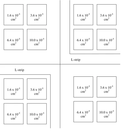
Three types of wafers were fabricated. The first of these was simply a blanket oxide
wafer and is referred to as a Blanket Wafer. The next two types have four arrays of four
different capacitor areas in each of the four quadrants, with the quadrants separated by a strip
of oxide with the same nominal thickness as the active areas. A schematic illustrating this is
shown in Figs. 3-1 and 3-2. The two wafers were different in that one had field oxide
isolated capacitors and the other had typical short-loop MOS capacitors. These wafers are
referred to as Hg-Caps and Poly-Caps, respectively.
Fabrication of the Blanket Wafer consisted of a JTB 100 clean [11], a ramp-up at
atmosphere in N2 with 1% O2, and a gate oxidation in a prototype vertical furnace at a
pressure of 985 mT and temperature of 850° C for 15 min. A monitor wafer was measured
optically using a KLA-Tencor UV-1280SE tool with a 121-point map that resulted in a mean
oxide thickness of 2.12 nm with a standard deviation less than 0.04 nm.
The Hg-Caps and Poly-Caps were processed at the same time. They were both
initially cleaned with a JTB 100 clean. Then a field oxide with a target thickness of 350 nm
was grown. The wafers were then annealed at 1000º C for 60 minutes. The active areas
the photoresist the wafers were cleaned using JTB 100. The gate oxidation was performed
with a prototype vertical furnace at 850º C for 15 minutes at a pressure of 985 mT. At this
point the Hg-Caps were completed on p-type wafers.
The n+ polysilicon gate electrode was then formed on the silicon oxide. Amorphous
silicon with a target thickness of 200 nm was deposited in the vertical furnace. A
phosphorous disk diffusion was done at 900º C for 30 minutes followed by a deglaze step.
Aluminum was then evaporated on the frontside of the wafer. The gate electrode was
defined with phototlithography and the aluminum and polysilicon were removed with a
chemical etch. The photoresist was removed and a buffered oxide etch was done on the
backside of the wafer before aluminum was evaporated on the backside of the wafer. These
steps were performed on both p- and n-type wafers and result in devices that are called
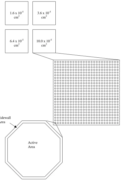
Figure 3-1 Wafer sized diagram of an Hg-Caps wafer showing the locations of capacitors of each area. Also shown is the L-strip, which has an oxide of the same thickness as the capacitors.
10.0 x 10⁻⁵ cm2 1.6 x 10⁻⁵
cm2
3.6 x 10⁻⁵ cm2
6.4 x 10⁻⁵ cm2
10.0 x 10⁻⁵ cm2 1.6 x 10⁻⁵
cm2
3.6 x 10⁻⁵ cm2
6.4 x 10⁻⁵ cm2 10.0 x 10⁻⁵
cm2 1.6 x 10⁻⁵
cm2
3.6 x 10⁻⁵ cm2
6.4 x 10⁻⁵ cm2
10.0 x 10⁻⁵ cm2 1.6 x 10⁻⁵
cm2
3.6 x 10⁻⁵ cm2
6.4 x 10⁻⁵ cm2
L-strip
Active Area Sidewall
Area
10.0 x 10⁻⁵ cm2 1.6 x 10⁻⁵
cm2
3.6 x 10⁻⁵ cm2
Chapter 4 The Extraction of a Statistically-Robust Active Area Oxide
Thickness from Overlapped MOS Capacitors
4.1 Introduction
The object of the analysis methodologies, experiments, and modeling presented in
this chapter is to determine the effects that the actual physical structure of an overlapped
MOS capacitor and the problematic etch bias have on the extraction of oxide thickness. As
device sizes are scaled down, these concerns become more pressing. Considerations were
taken into account for the overlap of the gate electrode outside of the active area, the angle of
the active-area sidewall, and the expansion of the active area due to an etch bias.
A MOS capacitor is usually modeled as a parallel plate capacitor (see Fig. 4.1-1a).
However, this model is not very accurate. The model does not take into account the
overlap of a gate electrode or the problematic sidewall geometry. Typical C-V
measurements result in the capacitance from a device that is defined by the gate electrode.
This includes capacitance from the active area, the gate electrode overlap, and, oftentimes, a
contribution from the sidewalls. Does this measured capacitance need to be reduced to the
capacitance of the active area alone? How does an etch bias change the extracted value of
oxide thickness? In order to answer these questions, it must be determined how these
additional contributions affect extracted tox values. The model in Fig. 4.1-1b shows a
capacitor with an overlap and non-vertical sidewalls. The contributions from the overlap and
angled sidewalls can be investigated using the classic definition of capacitance.
Additionally, if there is an etch bias during processing, the changes in tox values can be
In order to remove the contribution from the overlap, the area of the gate electrode
must be known. A good approximation of this area is usually sufficient. Knowing this area,
it is a simple matter of manipulating the measured data, with a series of equations and plots,
to reduce this total (i.e., as-measured) capacitance to that of the active area alone. The
overlap was studied using C-V characteristics from a metal/p Hg-Cap and both n+/p and n+/n
Poly-Caps with a nominal oxide thickness of 2.0 nm.
To study the sidewall contribution, the changing thickness must be tracked as it
increases from the active area to the field oxide. Since this involves a continuously changing
quantity, initial attempts were made to solve this with integration. Unfortunately the integral
never converged. Another approach that divided the sidewall into columns of different
thickness was used. Using these columns, the contribution of a non-vertical sidewall was
realized.
During processing, an etch bias may change the size of the active area. The
consequences of this bias to the extracted value of tox can be determined by simply enlarging
the active area and comparing the differences to the values of tox that are obtained from the
mask defined areas.
4.2 Gate Electrode Overlap
In order to determine the oxide capacitance (i.e., the capacitance from the active area
only), it must be realized that the total (i.e., as-measured) capacitance is the sum of three
In order to reduce this measured capacitance to the capacitance from the active area alone
(i.e., the oxide capacitance), a simple method is used as outlined below.
With the classical definition of capacitance, C = εoKA/t, where εo is the permittivity
of free space (8.85 x 10⁻¹⁴ F/cm2), K is the dielectric constant for SiO2 (3.9 is used here), A is
the area of the capacitor in cm2, and t is the thickness of the dielectric in cm, we see that, if
the active area of a device is zero, then the capacitance from the active area should be zero.
Using this fact and assuming vertical sidewalls, a plot of the measured capacitance, CTOT,
versus the mask defined active area, AM, should be linear and a fit to the data will result in an
equation of the form
where Co is the y-intercept with units of capacitance and the slope m is in units of
capacitance / unit area. As the active area goes to zero, the oxide capacitance goes to zero.
Using this along with equation (4.2-1), it can be seen that as AM goes to zero, Co is
approximately the maximum value of the field oxide capacitance (i.e., CFox).
Next the area of the gate electrode, Ag, must be determined. The area of the Hg-gate
(i.e., the Hg-probe used by the CV-Map 92A) is known to be 2.883 x 10⁻³ cm2. The areas of
the four Al/Poly-Si gates were calculated from optical images. The average areas are given
in Table 4-1 with the mask defined areas and the % difference.
Table 4-1 Gate electrode areas
Mask Defined Active Area
(x 10-5 cm2)
Average Gate Electrode Area from
Optical Microscopy (x 10-4 cm2)
Mask Defined Gate Electrode
Area (x 10-4 cm2)
% Difference
Overlap (x 10-4 cm2)
1.6 3.06266 3.105 1.36 2.945
3.6 3.50445 3.565 1.70 3.205
6.4 4.35288 4.375 0.51 3.735
10.0 5.26763 5.265 0.05 4.265
The active-area capacitance of the ith device is then extracted from the total capacitance with
the following equation
where AM-i is the mask defined active area of the ith capacitor. This correction is applied to
the entire voltage range of a data set in order to get the oxide capacitance curve. A plot of
the oxide capacitance at a given voltage versus the mask defined active area can then be used
to find the oxide thickness. The slope of a linear fit to this plot can be used to find the oxide
thickness from Tables A-1, -2 and –3 located in Appendix A.
The wafer IDs for the three wafers used are N-II-1 (Hg-Caps), K-III-1 (n+/p
Poly-Caps), and K-III-1-N (n+/n Poly-Caps).
4.2.1 Hg-Caps
Hg-characteristics for each capacitor area. The measured C-V Hg-characteristics are shown with the
CVC model fits in Fig 4.2.1-1. The model fit degrades as the capacitor area is reduced. The
measured capacitance at – 2.5 V was plotted versus the mask defined active area and is
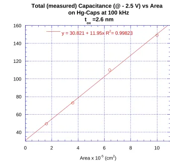
shown in Fig 4.2.1-2. The slope of the fit corresponds to an oxide thickness of 2.6 nm and
the y-intercept gives a Co of ~ 31 pF. The value Co is approximately the maximum value of
the field oxide capacitance and corresponds well to the value of 30.4 ± 1 pF measured on the
field oxide alone. The measured capacitance was reduced to the oxide capacitance as
described at the beginning of Section 4.2. The corrected average C-V characteristics for four
different area Hg-Caps are shown in Fig. 4.2.1-3 along with those modeled from the
corrected data. The extracted values of equivalent oxide thickness, tEOT, from the CVC
modeling program are shown in Table 4-2.
Table 4-2 CVC extracted tEOT from Hg-Caps characteristics
Mask Defined Active Area (x 10-5 cm2)
CVC tEOT from Total
Capacitance (nm)
CVC tEOT from Oxide
Capacitance (nm)
1.6 1.06 2.59
3.6 1.63 2.54
6.4 1.93 2.41
10.0 2.24 2.52
It can be seen in this table that the values of oxide thickness are more stable when using the
oxide capacitance in the model. Plots of the capacitance at – 2.5 V versus the mask defined
active area for these Hg-Caps were made with linear fits to the corrected and modeled data.
Figure 4.2.1-4 shows the linear fit for the oxide capacitance. The slope corresponds to an
oxide thickness of 2.58 nm and the y-intercept shows the capacitance of a zero-area device to
linear fit gives an oxide thickness of 2.58 nm. Including the gate electrode overlap results in
an increase in the extracted oxide thickness of 0.02 nm when extracted with the slope
method.
4.2.2 Poly-Caps
The n+/p and n+/n polysilicon capacitors were characterized with a standard probe
station connected to a HP 4284A LCR meter. Measurements were made in the parallel mode
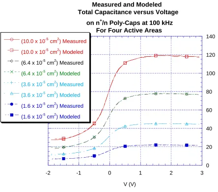
at 100 kHz. The average measured C-V characteristics from 10-20 n+/p Poly-Caps are
shown in Fig. 4.2.2-1, along with the modeled curves for each of the four areas. There is
very good agreement between the model and the total capacitance in both the accumulation
and depletion regions. The plot of total capacitance at – 2.5 V versus the mask defined active
area is shown in Fig. 4.2.2-2. From the slope of the linear fit, an oxide thickness of 2.36 nm
is predicted. From the y-intercept of this plot, the value for Co is ~ 4 pF. Figure 4.2.2-3
shows the corrected C-V characteristics with the modeled characteristics of the corrected
data. The modeled oxide capacitance curves show an excellent match throughout the voltage
range with a very small difference in the transition from depletion to inversion for the 10.0 x
10-5 cm2 case. Oxide thickness values extracted from CVC are given in Table 4-3.
Table 4-3 CVC extracted tEOT from n+/p Poly-Caps characteristics
Mask Defined Active Area (x 10-5 cm2)
CVC tEOT from Total
Capacitance (nm)
CVC tEOT from Oxide
Capacitance (nm)
1.6 1.91 2.41
Again, the oxide thickness values are more stable when using the oxide capacitance. Linear
fits to the capacitance at – 2.5 V versus the mask defined active area were performed on plots
of the corrected and modeled data for these Poly-Caps. The slope of the linear fit for the
oxide capacitance versus area, shown in Fig. 4.2.2-4, returns an oxide thickness of 2.34 nm;
while the slope for the modeled oxide capacitance, shown in Fig. 4.2.2-5, returns an oxide
thickness of 2.33 nm. Again using the slope method, the capacitance of the gate electrode
overlap increases the equivalent oxide thickness by ~ 0.02 nm.
Similar plots are shown for the n+/n Poly-Caps in Figs. 4.2.2-6, -7, -8, -9, and -10 and
the same method of data acquisition was used. The measured capacitance and corresponding
modeled curves are shown in Fig. 4.2.2-6. There is excellent agreement between the
measured curves and the model fits. The slope of the linear fit to the plot of total capacitance
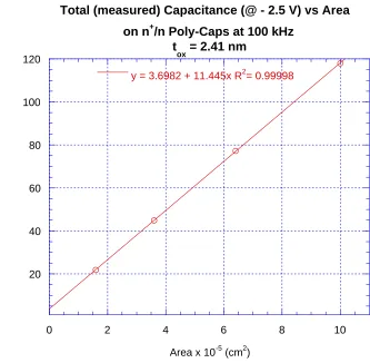
at 2.5 V versus the mask defined active area as shown in Fig. 4.2.2-7 gives an oxide
thickness of 2.41 nm and the y-intercept shows a Co of ~ 4 pF. The corrected and modeled
capacitance overlays are shown in Fig. 4.2.2-8. The modeled curves match very well in
accumulation and depletion for all areas and there is only a slight deviation in the inversion
region. The CVC extracted oxide thickness values for both the measured and corrected
capacitance are given in Table 4-4.
Table 4-4 CVC extracted tEOT from n+/n Poly-Caps characteristics
Mask Defined Active Area (x 10-5 cm2)
CVC tEOT from Total
Capacitance (nm)
CVC tEOT from Oxide
Capacitance (nm)
1.6 1.88 2.39
3.6 2.12 2.36
6.4 2.22 2.35
The oxide thickness values are more stable when using the oxide capacitance. The oxide
capacitance and modeled oxide capacitance at 2.5 V are plotted versus the mask defined
active area in Figs. 4.2.2-9 and 4.2.2-10 and have similar slopes that correspond to oxide
thickness of 2.4 nm. Using the slope method, the oxide thickness extracted from the total
capacitance curve results in an increase in equivalent oxide thickness of 0.01 nm.
From the data presented, it is seen that the overlap increases the equivalent oxide
thickness by ~ 0.02 nm when the slope method is used. From Tables 4-2, -3, and –4, it is
observed that as the active area of the capacitor decreases there is a significant increase in the
difference between the methodologies of extracting oxide thickness from the as-measured
and the corrected capacitance. Table 4-5 shows the differences between extracted metrics
and the methodologies for each type of capacitor including the y-intercept (Co), the slope
(m), the equivalent oxide thickness (tEOT) corresponding to the slope, and the R2 value of the
linear fit.
Table 4-5 Analysis methodology and extracted metrics
Capacitor Type Methodology Co (pF) Slope (µF/cm2) tEOT (nm) R2
CTOT vs AM-i 30.8 1.195 2.60 0.9982
Cox vs AM-i 0.15 1.202 2.58 0.9981
metal / p Hg-Caps
Cox.Mod vs AM-i 0.0036 1.203 2.58 0.9984
CTOT vs AM-i 4.06 1.212 2.36 0.9999
Cox vs AM-i 0.090 1.222 2.34 0.9999
n+ / p Poly-Caps
Cox.Mod vs AM-i 0.036 1.223 2.33 0.9998
CTOT vs AM-i 3.70 1.145 2.41 0.9999
Cox vs AM-i 0.16 1.150 2.40 0.9999
n+ / n Poly-Caps
From this table it can be seen that the maximum overlap capacitance for the Hg-probe is ~ 30
pF which is in excellent agreement with the average measured value of the field oxide
capacitance for all four quadrants of 30.4 +/- 1 pF. The maximum overlap capacitance for
the Poly-Caps is ~ 4 pF and using the average gate electrode area, the classical definition
yields a thickness of ~ 350 nm which is comparable to the target field oxide thickness of
360.0 nm. The Co values obtained using the corrected capacitance are all close to zero. The
difference from zero is attributed to statistical variations related to spatial variations,
non-vertical sidewalls and an etch bias.
The inflection point of both the as-measured and corrected characteristics from a 10.0
x 10-5 cm2 capacitor was used to extract the flatband voltage. Table 4-6 summarizes the
results.
Table 4-6 Flatband voltage from measured (CTOT) and corrected (Cox) C-V characteristics
Capacitor Type Flatband Voltage from the Inflection Point
VFB from CTOT VFB from Cox ∆∆∆∆VFB (mV)
Hg-Cap – 0.785 – 0.783 2
n+/p Poly-Cap – 1.229 – 1.307 78
n+/n Poly-Cap – 0.088 – 0.005 83
It can be seen from the table that the differences in extracted flatband voltage from the
as-measured and corrected characteristics of the Hg-Cap is quite small, however, in the case of
the Poly-Caps, there is a difference of ~ 80 mV. The flatband voltages, determined by CVC,
for the four areas and four gate oxide thicknesses are located in Appendix D. Of special note
is the differences in oxide thickness, ~ 0.25 nm, and in flatband voltage, ~ 500 mV, between
the metal/p Hg-Caps and the n+/p Poly-Caps. As is demonstrated in Chapter 5, this
4.3 Sidewall Contributions
As stated earlier, an overlapped capacitor contains three areas and each area has a
different thickness. These are the active area, the field oxide, and usually a sidewall. This
device structure can be modeled as three capacitors in parallel, specifically, the capacitors
formed by the active area (Cox), by the overlap of the gate electrode on the field oxide (CFox),
and by the sidewall (CSW). The first two terms are calculated simply with the classic
equation C = εoKA/t, with tox used for the gate oxide, tFox for the field oxide, and K = 3.9.
Two assumptions are used to simplify the calculations for the sidewall capacitance.
First, the octagonal capacitor is assumed to be a square of the same area and, second, the
sidewall is assumed to encroach equally upon the field and active areas.
With these assumptions the active area, Aa, is reduced to
and, for a Hg-gate capacitor, the area of the field oxide, AFox, is
where AMask is the mask defined active area and AHg is the area of the Hg-probe. For a
typical Al/Poly-Si overlapped capacitor similar changes are needed with the exception of
using the area of the gate electrode in place of the area of the Hg-probe. With these changes
to the respective areas, the field oxide capacitance, CFox, and the gate oxide capacitance, Cox,
can be found using the classic definition.
(4.3-1) Aa =[AMask − (tFox −tox)]
/
1 2 1
2
2
(4.3-2)
A
Fox=
A
Hg−
[
A
Mask1 2/+
1(
t
Fox−
t
ox)]
2
The capacitance from the sidewalls is slightly more difficult. Since the classical
capacitance is a function of the ratio of area to thickness, the following integral was used to
calculate the sidewall capacitance.
A relation between the area and the thickness must be established in order to solve this
integral. From the capacitor model being used, shown in Fig. 4.3-1, the sidewall area, ASW,
is related to the thickness by ASW = Aa½ [(t-tox)/tan θ]. Using a 45º sidewall, this becomes
ASW = Aa½ (t – tox). The capacitance of the sidewalls, not including the corners is
and the capacitance of the corners is
The capacitance of the entire sidewall is then the sum of these two quantities.
Therefore the total capacitance becomes
(4.3-6) .
CSW =CS +CC
(4.3-7)
The initial attempts to integrate the capacitance resulted in a sidewall capacitance much less
than if the sidewalls were vertical, so another approach was taken.
The sidewall was divided into a countable number of wedges of set width. The
number of wedges needed to account for the entire sidewall is the perimeter of the active area
divided by the chosen width of the wedge. Here a width of 1 nm was chosen to avoid areas
close to the area of an individual molecule.
In the simple case of a vertical sidewall, the entire wedge is considered to be the same
thickness as the field oxide. The capacitance is simply C = εoKWL/t, where W is the width
of the wedge and L is the length of the wedge. The length is the difference between the
thickness of the field oxide and the gate oxide.
For the 45° sidewall case, the wedge is broken into 1 nm x 1 nm columns. The
thickness of each column increases by 1 nm / column as they are advanced from the active
area to the field. This is shown graphically in Fig. 4.3-2. The capacitance of the wedge is
then the sum of the capacitance from each column since the columns act as capacitors in
parallel.
The capacitance from the entire sidewall is the capacitance of the wedge multiplied
by the number of wedges needed to encompass the perimeter of the active area. By using
wedges, the approximate capacitance for the sidewall of a capacitor of any area on the wafer
can be easily determined once the capacitance of the wedge is known.
small resulting in a percent difference that is less than 0.02 %. Even in the case of the 10.0 x
10-5 cm2 device with 45° sidewalls, the contribution is on the order of 30 fF. In Fig. 4.3-4,
the slope of the total capacitance versus area is shown for the 45° and 90° sidewalls. The
slopes of the linear fits are identical. The slope returns an oxide thickness of 2.01 nm. A plot
of the difference in the two capacitances (i.e., 45° – 90°) versus active area is shown in Fig.
4.3-5. Fitting a third-order polynomial, with capacitance in pF and area x 10-5 in cm2, to the
points results in
C = 1.13 x 10⁻⁵ A3 – 2.95 x 10⁻⁴ A2 + 4.03x 10⁻³ A + 5.22 x 10⁻³
with an R2 = 1. Calculations made for areas of 1.6, 3.6, 6.4, and 10.0 x 10⁻⁵ cm2 result in
sidewall capacitance differences between 10-30 fF as shown in Table 4-7.
Table 4-7 Capacitance difference of vertical to non-vertical sidewalls
Mask Defined Active Area (x 10-5 cm2) Difference of 90º to 45º Sidewall (fF)
1.6 10.9
3.6 16.4
6.4 21.9
10.0 27.4
From these results, it is seen that using the assumption of vertical sidewalls is a very good
approximation except for large active areas (i.e., much greater than 10.0 x 10⁻⁵ cm2).
4.4 Etch Bias
A potential problem in the extraction of tox is the ‘unknown’ effect of an etch bias.
This effect was investigated by mathematically enlarging the active area to simulate over
etching. The active area was enlarged by 1% and 5% of a 10.0 x 10⁻⁵ cm2 capacitor. The
calculated using C = εoKA/t. The thickness used for the field oxide was 360.0 nm while the
gate oxide thickness was 2.0 nm. The area of the gate electrode was set to 2.883 x 10⁻³ cm2.
Here the value of 3.9 is assigned for the dielectric constant. The sidewall angle is assumed to
be vertical. The total capacitance is then the sum of the capacitance from the field and the
gate.
Linear fits were done for the total capacitance, Fig. 4.4-1, and the oxide capacitance,
Fig. 4.4-2, versus active area without an etch bias and with the two etch biases. The slope of
the linear fit to the total capacitance corresponds to an oxide thickness of 2.04 nm, while the
linear fit to the oxide capacitance gives an oxide thickness of 2.03 nm. With a 1% etch bias
the slopes of capacitance versus area return oxide thickness values of 2.04 nm and 2.02 nm
for the total capacitance and the oxide capacitance, respectively. Using a 5% bias returns
oxide thickness values of 2.03 nm and 2.02 nm for total and oxide capacitance, respectively.
This shows that an etch bias has a negligible effect on the slope method of
determining the oxide thickness (i.e., ∆tEOT ~ 0.01 nm). There is little effect since the
calculated capacitance has a linear relation to the area and both etch biases were assumed
constant regardless of the size of the active area. If this was not the case, then the physical
metrics that are summarized in Table 4-5 would be unphysical and the statistical metric (i.e.,
(a)
(b)
Figure 4.1-1 Schematic drawings of MOS capacitor
(a) Typical parallel plate model
(b) Model incorporating the gate electrode overlap and non-vertical sidewalls
Gate Electrode
Gate Oxide
Si Substrate
Gate Electrode
Gate Oxide
Field Oxide
Figure 4.2.1-1 Plot of measured and modeled oxide capacitance versus voltage as a function of area for the average values of 10-20 Hg-Caps. There is excellent agreement in the accumulation region.
20 40 60 80 100 120 140 160
-3 -2 -1 0 1 2
Measured and Modeled Total Capacitance versus Voltage
on Hg-Caps at 100 kHz Four Active Areas
(10.0 x 10⁻⁵ cm2) Measured
(10.0 x 10⁻⁵ cm2) Modeled
(6.4 x 10⁻⁵ cm2) Measured
(6.4 x 10⁻⁵ cm2) Modeled
(3.6 x 10⁻⁵ cm2) Measured (3.6 x 10⁻⁵ cm2) Modeled
(1.6 x 10⁻⁵ cm2) Measured
(1.6 x 10⁻⁵ cm2) Modeled
T
o
tal
C
apaci
tance (
p
F
)
Figure 4.2.1-2 Total capacitance at – 2.5 V versus mask defined area for Hg-Caps. The slope of the linear fit corresponds to an oxide thickness of 2.6 nm and the intercept shows a field oxide contribution of ~ 31 pF.
40 60 80 100 120 140 160
0 2 4 6 8 10
Total (measured) Capacitance (@ - 2.5 V) vs Area on Hg-Caps at 100 kHz
t
ox =2.6 nm
y = 30.821 + 11.95x R2= 0.99823
Tot
a
l Capac
it
anc
e (pF)
Figure 4.2.1-3 Plot of corrected and modeled oxide capacitance versus voltage as a function of area for the average values of 10-20 Hg-Caps. There is excellent agreement in the accumulation and depletion regions.
0 20 40 60 80 100 120 140
-3 -2 -1 0 1 2
Corrected and Modeled Oxide Capacitance versus Voltage
on Hg-Caps at 100 kHz For Four Active Areas
(10.0 x 10⁻⁵ cm2) Measured
(10.0 x 10⁻⁵ cm2) Modeled
(6.4 x 10⁻⁵ cm2) Measured
(6.4 x 10⁻⁵ cm2) Modeled
(3.6 x 10⁻⁵ cm2) Measured
(3.6 x 10⁻⁵ cm2) Modeled
(1.6 x 10⁻⁵ cm2) Measured
(1.6 x 10⁻⁵ cm2) Modeled
Oxide Capacit
ance (
p
F)
Figure 4.2.1-4 Plot of the oxide capacitance at – 2.5 V versus area for the average values of 10-20 Hg-Caps. The slope of the linear fit corresponds to toxcorrected = 2.58 nm.
The intercept shows the capacitance for a zero area device to be 0.15 pF. 20
40 60 80 100 120 140
0 2 4 6 8 10
Oxide Capacitance (@ - 2.5 V) vs Area on Hg-Caps at 100 kHz
t
ox corrected
= 2.58 nm
y = 0.15301 + 12.023x R2= 0.99812
O
x
ide Capac
it
anc
e (pF)
Figure 4.2.1-5 Modeled oxide capacitance at – 2.5 V versus mask defined active area for Hg-Caps. The slope gives an oxide thickness of 2.58 nm, which agrees with Figs. 4.2.1-2 and 4.2.1-4, and the intercept shows a capacitance of ~ 4 fF at zero area.
20 40 60 80 100 120 140
0 2 4 6 8 10
Modeled Oxide Capacitance (@ - 2.5 V) vs Area on Hg-Caps at 100 kHz
t
ox corrected
= 2.58 nm
y = 0.0036145 + 12.027x R2= 0.99848
Modeled O
x
ide Capac
it
anc
e (pF)