ABSTRACT
HYUNGTAK SEO. Characterization of High-k Dielectrics and Interfaces on Device Reliability. (Under the direction of Gerald Lucovsky).
Transition metal and rare earth elemental and complex oxide high-k dielectrics and their interfaces with Si and Ge substrates were investigated in an effort to (i) understand the physical origin of intrinsic pre-existing, and extrinsic process-induced defects and to thereby (ii) achieve enhanced reliability in advanced devices such as metal oxide semiconductor capacitors and field effect transistors, MOSCAPs and MOSFETs, respectively.
Intrinsic pre-existing bonding defects in nanocrystalline high-k dielectrics are associated with discrete energy states near the conduction and valence band edges. These defects are localized at nanocrystalline grain boundaries and have been detected by measurements based on several different spectroscopic techniques including soft X-ray absorption and photoelectron spectroscopies, spectroscopic ellipsometry and internal photoemission spectroscopy. Estimated pre-existing defect densities in nanocrystalline high-k dielectrics by these spectroscopic measurements are typically of order 1012 cm-2 in films that are more than 3 nm thick, but can be reduced by about an order of magnitude in noncrystalline HfSiON dielectrics, and in nanocrystalline films that are ≤ 2nm thick.
Ni-doping into BaSrTiO3 (BST) changes the local bonding distortion by partial replacement of Ti3+ atoms with Ni2+ in divacancy defect states. This reduces the defect density by a factor of five to seven-fold and shifts the defect states closer to the conduction band edge by ~ 0.3 eV compared to undoped BST. A significant enhancement of metal-insulator-meta (MIM) capacitor reliability was achieved by suppression, and recovery of symmetry in the MIM leakage current. This increased resistance to dielectric breakdown by shifting the onset by more than 20 V.
Characterization of High-k Dielectrics and Interfaces on Device Reliability
by
Hyungtak Seo
A dissertation submitted to the Graduate Faculty of
North Carolina State University
In partial fulfillment of the
Requirements for the degree of
Doctor of Philosophy
Electrical Engineering
Raleigh, North Carolina
2008
APPROVED BY:
DEDICATION
BIOGRAPHY
ACKNOWLEDGEMENTS
First of all, I would like to thank the advisory committee members, Dr. Gerald Lucovsky, Dr. Carl Osburn, Dr. David Aspens, and Dr. Veena Misra for their generous guidance and review on this work. Their guidance from the very first time when I started Ph.D. study made not only my work but life in NCSU much better and more complete. I would like to give my special thanks to my advisor, Dr. Gerald Lucovsky. He has always been ahead for giving a very correct direction to my study in a kind way. I have learned a lot of valuable and great knowledge and the way of thinking as a scientist but also as a person. I am absolutely sure that his teaching to me will be “the bible” for my work all my life.
I also would like to expand my thanks to my former and current colleagues, Dr. Kwonbum Chung, JP Long, Dr. Relja Vasic, Dr. Sanghyun Lee, Dr. Sang Jeong Oh, Nick Stoute. It was a great experience that I worked and enjoyed my time in the lab with all of you.
Personally, I owe lots of things to my friends in NCSU, Chulwoo Oh, Jiyoung Chung, Chanyeon Won, Sangtae Bae, Hoonseok Kim, Jeesung Chung, Dr. Taesik Han, Sangoh Han, Byungdon Kong, Byungil Kwak, Jinseok Park, Bongmook Lee and all people who I know even though they are not listed here, for their friendship. I will not forget the precious time with you.
TABLE OF CONTENTS
Page
LIST OF FIGURE……….…vii
1 Introduction………..…..………...1
1.1 Need of High-k Dielectrics in Scaled Down CMOS and Memory Circuits……...1
1.2 Reliability Issues of High-k Dielectric Gate Stacks……….…....4
1.3 Intrinsic Chemical and Physical Properties of TM/RE Oxides……….…….…5
1.4 Crystal-Field and Jahn-Teller Term Splitting…………..…………...……….…...…..6
1.5 Spectroscopic Techniques: XAS and SE………...…..9
1.5.1 X-ray Absorption Spectroscopy (XAS) ...……..………9
1.5.2 Spectroscopic Ellipsometry (SE)………..………11
1.6 Electrical Techniques: C-V and I-V………..………16
1.7 Overview of Dissertation………...17
1.8 References……….…….19
2 Spectroscopic Defection of Defects present in TM/RE Elemental/Complex High-k Oxides………….………..………..….28
Abstract……….………..28
2.1 Introduction……….……….29
2.2 Experimental Procedures………..29
2.3 Results and Discussion………..………..……….30
2.3.1 Defects in TiO2 and HfO2……….……30
2.3.2 Defect Suppression in Ti- and Hf-Si oxynitrides………..…………33
2.4 Summary….……….………36
Page
3.4 Conclusions……….……….56
3.5 References…….………..57
4 Defect Band Engineering of BaSrTiO3 Dielectrics in Metal Insulator Metal Capacitor by Ni Doping……..………..………...……68
Abstract……….………..………...68
4.1 Introduction……….………….69
4.2 Experimental Procedures………..69
4.3 Results and Discussion……….70
4.4 Conclusions……….………....75
4.5 References………..76
5 Preparation of Native Oxide and Carbon Minimized Ge surface by NH4OH Cleaning for Deposition of High-k Dielectrics ……….……….…...84
Abstract………..……….………..……...84
5.1 Introduction……….……….….85
5.2 Experimental Procedures………….………..86
5.3 Results and Discussion……….……….87
5.4 References……….………..…………93
6 Correlation Between Defects identified by Spectroscopic Measurements and charge Trapping at Ge/HfO2 and HfSiON Interfaces with GeON Layer……...………...99
Abstract……….………..……...99
6.1 Introduction………..……….….100
6.2 Experimental Procedures…….………..……….101
6.3 Spectroscopic Identification on Defects: MEIS, SE, and XAS Results……….102
6.4 Electrical Properties of Hf based High-k on Ge……….……...106
6.5 Summary………..…………...………...….…..112
LIST OF FIGURES
Page Fig 1.1. Electronic band edge diagrams of SiO2 (left) and TM/RE high-k oxides (ZrO2, right) constructed by molecular orbital (MO) theory………...…..22
Fig 1.2. Schematic CB and VB band edge MO states in TiO2………....23
Fig. 1.3 . Schematic d-state evolution in TiO2 and HfO2 consisting of CB edge states.….….24
Fig. 1.4. Schematic scheme of spectroscopic measurements on TM/RE oxides…………....25
Fig. 1.5. Schematic diagram of the ellipsometry (top) and the ellipsometric modeling process……….26
Fig. 1.6. (a) Schematic diagram of the pseudodielectric function. (b) On left, what model assumes (electromagnetically sharp interface). On right hand side, what is encountered in reality (interface layers, contamination, surface roughness)………..…27
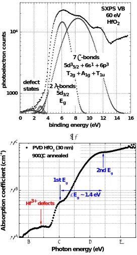
Page Fig. 2.4. (a) SXPS VB structure versus binding energy and (b) VUV SE ε2 spectrum versus photon energy for HfO2……….42
Fig. 2.5. Band edge and pre-existing defects determined by spectroscopic studies for (a) HfO2 and (b) TiO2………..…….43
Fig. 2.6. O K1 and ε2 spectra for low and high Si3N4 content Ti Si oxynitride alloys….….…..44
Fig. 2.7. ε2 spectra for (a) low- and (b) high-Si3N4 content Hf-Si oxynitride alloys before and after annealing………..……..45
Fig. 2.8. Schematic representation of local bonding arrangement in optimized Zr(Hf)-Si oxynitride alloy with ~33-40 % Si3N4, and 30-33 % SiO2 and HfO2………...46
Fig. 3.1. Sc L3 edge XAS spectra for (a) as-deposited and (b) 1000 °C annealed nanocrystalline LaScO3...59
Fig. 3.2. O K1 edge XAS spectra for (a) as-deposited and (b) 1000 °C annealed nanocrystalline LaScO3………...60
Fig. 3.3. La M2,3 edge XAS spectra for (a) as-deposited and (b) 1000 °C annealed nanocrystalline LaScO3……….………..…..61
Page 1000°C annealed LaScO3 thin film………..63
Fig. 3.6. Imaginary part of the complex dielectric constant versus photon energy for as-deposited and annealed LaScO3 thin films between 700 and 1000 °C……….……...64
Fig. 3.7. HRTEM images of (a) as-deposited and (b) 1000°C annealed LaScO3…….……..65
Fig. 3.8. Band edge PC for nano-crystalline as-deposited LaScO3 film………..……..66
Fig. 3.9. (a) XAS O K1 edge spectrum and (b) VUV SE spectra for 0.38 nm of LaAlO3 on SrTiO3 for different oxygen pressure in film deposition………..………..67
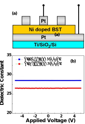
Fig. 4.1 (a) schematic representation of MIM (Pt/Ni-BST/Pt) capacitor. The bottom Pt electrode is placed on Ti/SiO2/Si stack which emulates the actual layers in DRAM storage cell and (b) Dielectric constants of MIM capacitor extracted from high-frequency (1 MHz) C-V analysis with Ni-doped and undoped BST dielectrics. The undoped BST showed the slightly higher dielectric constant. There was no significant dielectric loss across the applied voltage………..…78
Page Fig. 4.4. Local bonding of Ti-atoms (gray) and O-atoms (black) in i) undistored octahedral arrangements in which all bond lengths, ax, ay and az are equal, ii) orthorhombic arrangements in which all bond lengths are unequal, and iii) in tetragonal arrangements with two equal bond lengths………81
Fig. 4.5. Schematic energy band diagram for conduction band empty anti-bonding states, and band edge defects states for undoped and Ni-doped BST obtained from analysis of ε2 spectra. Solid lines, and bold face energy level positions, and energy differences reflect strong features in ε2, whereas, dashed lines, and plain text indicate significantly weaker spectral features………....82
Fig. 4.6. Band alignment for that includes band edge defects in undoped (heavy solid line) and Ni-doped (dashed line) BST MIM capacitors. The Pt 6s state Fermi level is indicated metal gate Fermi levels are indicated, as well as the Pt 5d state filled band. Transport processes are indicated by arrows beginning in the Pt electrodes of the cathode (negative) and differentiated by the character of these arrows……….……83
Fig. 5.1. The plot for Imaginary parts of pseudo dielectric function for (100) Ge surfaces with and without different surface treatment: NH4OH-based, HF-based, H2O2/HF, and No treatment (Bare wafer)………..95
Fig. 5.2. The plot for GeO2 thickness evolution during the NH4OH-based surface treatment for (a) (111) and (b) (100) Ge surfaces. The GeO2 thickness was extracted from the real-time SE measurements with cleaning process………..96
Page surface treatments: Bare, HF-, and NH4OH-based cleaning. For wide energy scan, there are energy peak states associated to germanium (45~50 eV), carbon (268 eV) and oxygen (509 eV) species. For narrow energy scan, there are Ge peaks related to two different bonding states, Ge-O (44 eV) and Ge-Ge (48 eV)……….…….98
Fig. 6.1. Compositional depth profile obtained by simulating MEIS energy spectra for as-deposited and annealed (a) HfO2 films and (b) HfSiON films on Ge(100) substrates. Dotted line and arrow indicate the Ge substrates and the direction of the films. The spot with the error bar represents the fitting error in the depth direction and the relative concentration..115
Fig. 6.2. Imaginary dielectric function (ε2) spectra from SE measurement for as-deposited and annealed HfO2 and HfSiON films on Ge(100) substrates. D1 and D2 indicate the defect states located below the conduction band edge…….……….116
Fig. 6.3. XAS spectra below the absorption edge of the O K1 feature for (a) HfO2 and (b) HfSiON films on Ge(100) substrates. Two deconvoluted peaks, labeled D1 and D2, indicate the defect states determined by Gaussian fitting of the XAS O K1 edge spectra…….…….117
Fig. 6.4. Relative strengths of defect features determined from Gaussian fits to O K1 edge spectra………...118
Page Fig. 6.8. Plot of NEFF as a function of Ninj for as deposited and annealed HfO2 and HfSiON………..122
Fig. 6.9. The relation between the oxide trapped charge density, Not and VFB extracted from C-V hysteresis as a function of PDA temperature for (a) HfSiON and (b) HfO2………123
Fig. 6.10. J-V plots for test devices with (a) as deposited and (b) 650 °C annealed HfSiON and (c) as deposited and (c) 600 °C annealed HfO2. There is an enhancement of leakage current characteristics for each annealed device compared to the as deposited………….124
Fig. 6.11. J-V plot for test devices with as deposited and 900 °C annealed HfSiON on SiON/Si. The HfSiON was deposited in the exactly same recipe as high-k/Ge devices…..125
Fig. 6.12. (a) Band alignments between (i) n-type Ge, GeO2 and HfO2 and (ii) n-type Ge, Ge3N4 and HfO2 and (b) substrate injection for an n-type Ge, GeO2 and HfO2 stack in (a), with and Al gate electrode, for which the conduction band offset energy between Ge and GeO2 which is less than that between Ge and HfO2, and for a gate stack on n-Si and with an SiON interfacial region, which is greater than that between Si and HfO2……….……..126
1 INTROUDCTION
1.1 Need of High-k Dielectrics in Scaled Down CMOS and Memory Circuits
After enormous growth of the semiconductor industry over several decades, microelectronics technology is facing the one of the most significant challenges in its history. The SiO2 layer in metal oxide semiconductor field effect transistor (MOSFET), which was regarded as “a gift from nature”, is rapidly approaching its physical limit due to direct tunneling [1,2]. The aggressive effort to achieve faster and more functional chips continued to scale the SiO2 or SiON dielectric thickness as gate lengths are scaled down. This effort to integrate the thinner gate oxides is derived from the physical scaling benefits in MOSFETs such as higher switching speed or less delay time, less power consumption, and higher density of transistors. It is clear to understand this relationship between improved transistor performance (transient response time of transistor switching, τ, and oxide capacitance, Cox, and saturation drain current, ID,sat) scaling factors from following simple MOSFET governing equations:
sat D
DD load
I
V
C
,
⋅
=
τ
1.1ox
source bias, and VT is the threshold voltage.
This advanced MOSFET processing technology requires gate oxide thickness less than 1.5 nm and extending below 1 nm [3]. However, SiO2 based gate dielectric has been supposed to reach a physical limit beyond 45 nm gate length MOSFET technology [4]. The level of ultra thin SiO2/SiON suffers from the direct tunneling through gate stacks. At these thicknesses, SiON has a direct tunneling current of greater than 103 A/cm2 for high-performance logic chips and 0.1 A/cm2 for low power chips [3].
Therefore, SiO2 or SiON might not be used toward MOSFETs with gate oxide thickness less than 1 nm. The solution for this limitation has been investigated by a replacement of gate oxide from SiO2 to high-k dielectrics in the material context of transition and rare earth elemental/complex oxides [5-7]. As noted in Eq. 1.1~1.3, benefits from replacement of gate dielectrics in MOSFETs by high-k dielectrics are multiple and significant: (i) suppression of leakage current by using physically thicker films while maintaining same equivalent oxide thickness (EOT) although there might be limited suppression of leakage current level mitigated by the lowered barrier height and (ii) increase of drain current by raising oxide capacitances.
equivalently to < 1 nm EOT of gate dielectrics [3]. In addition, logic chip groups requiring high performance of devices such as central processing units for computers also need the high-k dielectrics for boost of drain current in scaled down transistors. Secondly, memory devices such as dynamic random access memory (DRAM) and flash memory demand high-k dielectrics both for gate and capacitor regions. The future technology of flash memories such as charge trapping flash (CTF) will require several special specifications of (i) tunnel oxides and (ii) trapping oxides [10,11]. Tunnel oxides should have the thinner EOT and higher tunneling process for faster responses and longer retention time but at the same time, lower barrier height for effective tunneling process. Trapping oxides should have the high trapping efficiency which should be controlled by gate bias only. DRAM really relies on the specification of stacked metal-insulator-metal (MIM) capacitors for charge storage. The insulator should be thin enough to store an enough amount of charge (25fF/cell) while maintaining reasonable retention characteristics [3]. Therefore, high-k dielectrics are necessary for future advanced logic and memory devices.
1.2 Reliability Issues of High-k Dielectric Gate Stacks
Although significant efforts have been made to integrate high-k dielectric into advanced devices for the last 10 years, the introduction of high-k gate dielectrics has been delayed from the initial roadmap projection since they have several inferior intrinsic properties compared to SiO2 which turned out to deteriorate the device performance and reliability [12,13]. Major problems for the integration of high-k dielectrics to MOSFETs are listed as (i) leakage current levels which is not solely dependent on physical oxide thickness, (ii) surface dipoles or defects present close to the interface of poly-Si gate/high-k gate dielectrics invoking Fermi level pining, (iii) lowered channel mobility compared to the universal mobility, and finally (iv) fast charge trapping and trap creation resulting in threshold hysteresis and threshold voltage instability. These problems are considered to be very closely related to the presence of defects in high-k gate dielectrics after many studies.
The observed problems raised serious reliability concern for poly-Si gated devices employing high-k dielectrics. Frequently, one might be told things: “simple replacement of high-k dielectrics to SiO2 never works at all” and “only one good thing about high-k dielectrics is its high k value”. Later, however, high-k dielectrics in the gate stacks were used with new material integration, metal gate electrodes [13]. The use of metal gate was really effective to achieve more reliable novel gate stacks with high-k dielectrics than poly-Si/high-k gate stacpoly-Si/high-ks although it created other issues such as flat band voltage tuning (specially for pFETs) and metal/gate stack interface transformation after anneal [14,15].
life time”. Several critical studies in this specific topic reported multiple effects of metal gate on long term reliability: (i) metal gates reduce the delay between soft and hard breakdown of gate stacks and (ii) metal/oxide interfaces are subject to the severe degradation by the re-growth or chemical reactions after thermal processing. Thus, interfaces of metal/high-k gate stacks are recently being considered as a main issue on the reliability [16].
However, the ultimate interest on reliability of high-k dielectrics is to understand the physical origin and properties of intrinsic defects present in oxides and to obtain the engineering pathway for suppression of defects. For this specific study on high-k dielectrics, the basic review on the intrinsic physical and chemical characteristics is essential.
1.3 Intrinsic Chemical and Physical Properties of TM/RE Oxides
result in an asymmetric charge distribution between metal and oxygen which invokes additional ion off-center displacement arising increase in (i) polarizability and (ii) k values [18]. Because of this ionic interaction/overlapping between metal d-states and oxygen p-states, bandgaps of high-k dielectrics are typically lower than other amorphous oxides such as SiO2 and Si3N4 and tend to be decreased for TM/RE oxides with higher k values [19].
Another crucial physical property of TM/RE oxides is the sensitivity of d-states to the local bonding environments [17]. Thin film structures of TM/RE in high-k dielectrics of interest for device applications suffer from crystal structure transformation with anneals at different temperature. This is because d-states are sensitive to the changes and distortions in local bonding which will be discussed in the next section. The Inherent strong localization of electron distribution in d-states tends to be susceptible to the bonding distortion associated with the global structure changes that occur with thermal energy and mechanical strain at grain boundaries so that asymmetric bonding configurations are very common in thin film nanocrystalline TM/RE oxides.
Therefore, in contrast to the conventional amorphous gate dielectrics such as SiO2 and Si3N4, TM/RE high-k oxides are subject to crystallization, bonding distortion and defects, and, therefore, intrinsic VB/CB band edge energy states tend to change which sometime induce band gap changes, as in LaScO3 thin films [20].
1.4 Crystal-Field and Jahn-Teller Term Splitting
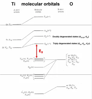
electron(s) in diatomic molecule environment [21]. Most commonly, an MO is represented as a linear combination of atomic orbitals (the LCAO-MO method). Because of such nature of MO theory, it is more effective to explain strongly localized bonding types [17,22]. This is the reason that MO theory is regarded as the best model to describe the electronic band structures of TM/RE oxides since they have the localized MO states between partially filled TM/RE d-states and oxygen 2p states. Figure 1.2 represents the schematic CB and VB band edge MO states in TiO2. In CB edge, there are triply degenerate T2g states (dxy, dyz, and dzx) in π anti-bonding characteristic and doubly degenerate Eg states (dx2-y2 and dz2) in σ anti-bonding characteristic respectively. In the VB edge, these MO states are located in mirror symmetry but the top of the valence band edge is dominated by non-bonding oxygen 2p states. Depending on bonding structures, the energy locations of T2g and Eg are reversed. For example, HfO2 has the lower-lying Eg and higher-lying T2g states in energy.
electrostatic perturbation of the transition metal d orbitals and the surrounding anions (e.g. oxygen atoms) [17, 23]. The previous case is applied to local structures having all equivalent bonding lengths between metal and oxygen. There can be asymmetric distortion in unit cells. In the case of HfO2, the distorted cubic bonding at asymmetric bonding lengths (i.e., ax ay az leads to multiplicities of d-states with complete degeneracy removal with the larger term split energies. This is called Jahn-Teller distortion (J-T) according to which a non-linear molecule in an electronic state with orbital degeneracy will distort so as to lower its symmetry and remove the degeneracy [24]. This case for HfO2 is described by evolution in the left hand side direction in Fig. 1.3. The evolution for right hand side direction corresponds to the octahedral (6-fold) metal-oxide bonding environment of TiO2, LaScO3, and LaTiO3.
oxides before device integration of high-k dielectrics.
1.5 Spectroscopic techniques: X-ray absorption spectroscopy (XAS) and
spectroscopic ellipsometry (SE)
In this section, several spectroscopic techniques employed in this study are addressed. XAS and SE techniques can probe the empty states by the transition from occupied states (core level for XAS and top of valence band for SE) to empty states in conduction bands. The schematic schemes of spectroscopic measurements on TM/RE oxides are shown in Fig 1.4. Although not discussed here, the occupied states in VB can be traced by Soft X-ray photoemission spectroscopy.
1.5.1 XAS
absorption near-edge structure (XANES) spectral region and the extended X-ray absorption fine structure (EXAFS) region. In the current study, measurements of XAS spectra on XANES spectral region are mainly conducted.
The XANES spectra are unique to the oxidation state and species of the element of interest, as such are used to determine the oxidation state and coordination environment of materials. In the current study, there two types of transition of interest: (i) the inter-atomic transition from occupied core level of OK1 edge to empty conduction band states of metal d-, s-, and p- states mixed with oxygen p- states and (ii) intra-atomic transition from metal core p- states to empty conduction band states [20].
spectra [25].
In the current study, XAS measurements were performed at the National Synchrotron Light Source (NSLS) at the Brookhaven National Laboratory (BNL), and at the Stanford Synchrotron Radiation Laboratories (SSRL) at the Stanford Linear Accelerator Center (SLAC) using total photo-electron yield to determine the relative absorption strength of the spectral features associated with transitions from TM, RE, and O-atom core level states to empty conduction band-states [26]. The current research proved that the XAS technique is very effective to detect a length of nanocrystalline less than 4 nm, a physical detection limit of XRD that can determine the size of crystalline.
1.5.2 SE
It is crucial to investigate the energy band structure of high-k materials since it has a direct relationship to the tunneling current and trap level in the gate dielectrics. Several optical measurements, such as transmission, and reflection spectroscopy have been employed for this kind of research. Among these optical measurement tools, SE is a very effective tool to achieve dielectric function of material [27]. SE is optical characterization
These are related each other by electromagnetic characteristics. Figure 1.5 depicts the procedure of SE measurements.[29]
The material system that we consider for this research is the ideal 3 layer system of which the uppermost layer is the ambient, the middle layer is the thin film high-k dielectric in nm (10-9m) range, and the lower layer is the substrate, normally Si wafer. This application of SE requires the conversion of measured quantities associated with microscopic polarization phenomenon into the macroscopic sample properties of interest: thin film thickness, optical constant, compositions, properties, etc. In other words, we can not use ellipsometry to directly measure much of the information of interest. As a result, we need an “optical model” to bridge the gap. This model is an ideal mathematical representation of the sample that allows us to calculate its polarization state change in terms of physical properties like thickness, refractive index, and composition. For each sample,
ρ
is calculated to matchthe experimental data, using multilayer mathematical models that contain parameters, such as layer thickness or composition, which are independent of the parameters varied in the measurement.
For the theory of analysis on data from SE measurements on high-k dielectrics on substrates, it is needed to go over (i) two- and three-phase models and (ii) effective medium approximation.
(i) Two phase and three phase model
boundary, that the projection of k onto the boundary is the same for each medium, and
dispersion equation,
ε
2 2/ω
2k c
= . Reflection at a boundary usually involves the participation of 4 waves, since in general both leftward- and rightward-propagating waves exits on either side of the boundary. As it is more efficient mathematically to represent these waves by single amplitude components only, reflection is described in terms of electric field for s-polarized light and the magnetic field for p-polarized light [27,28].
If no overlayer are present on the substrate or if the uppermost overlayer is optically thick, then no back reflectance occurs from deeper within, and only the two materials denoted by subscripts s and a (substrate and ambient) are involved. This is a 2 phase situation. In this case, reflectances can be expressed in the analytic form:
sppd appd sppd appd i s o s sa s n n n n E E r + − = =
, ; 1.4
sppd a appd s sppd a appd s i s o p sa p n n n n E E r
ε
ε
ε
ε
+ − =, ; 1.5
which give the s- and p-polarized complex reflectances for the two-phase model.
sin2
φ
sin2φ
tan2φ
[(1ρ
)/(1ρ
)]2ε
ε
= + − +a
s 1.7
If there is a very thin overlayer on substrate, the situation is different from 2 phase case. In principle this becomes simply a matter of starting at the just inside the substrate at the boundary between the substrate and first overlayer, where the boundary conditions
0 = = r s r s H
E meaning no back reflection inside substrate apply, then calculate the field
amplitudes just across the boundary in the first overlayer, then applying the appropriate exponential factors to calculate the amplitudes at the other boundary of the first overlayer, the repeating process until the wave emerges into the ambient. Considering in addition propagation across the layer (j+1) assuming a thickness dj+1, if only three phases (substrate, overlayer, ambient) are present, the generic form of reflectance for either s-or p-polarized light is therefore given by:
so oa so oa soa r Zr Zr r r + + =
1 , 1.8
where Z = exp(2ikj+1,ppddj+1).
If the overlayer is extremely thin so that
λ
π
4
<<
d
, then analytic results can again beobtained.
, [1 4 cos ] a s o s a sa s s dn r r
ε
ε
ε
ε
λ
φ
− − += ; 1.9
]
sin
)
/
1
/
1
(
1
sin
)
/
1
/
1
(
1
cos
4
1
[
2 2 ,ε
ε
ε
φ
φ
ε
ε
ε
ε
ε
ε
ε
λ
φ
π
a s a a s o a s o s a sa p sin
r
r
+
−
+
−
−
−
+
=
; 1.10] ) cot )( ( ) )( ( cos 4 1 [ 2 a s a s o a o o s s a sa idn
ε
φ
ε
ε
ε
ε
ε
ε
ε
ε
ε
λ
φ
π
ρ
ρ
− − − − += . 1.11
pseudodielectric function
<
ε
>
is that quantity that would be calculated from the direct ellipsometric data usingρ
using the two phase model, that is, by ignoring the existence ofpossible overlayers. The advantage of
<
ε
>
is that it represents the data in a form more nearly related to the quantity of interest for materials analysis; the original dataρ
canalways be recovered by reapplying the two-phase model to calculate it form
<
ε
>
. The result is[ sin2 ]1/2
) ( ) )( ( 4
φ
ε
ε
ε
ε
ε
ε
ε
ε
ε
ε
λ
π
ε
ε
− − − − + >= < a s a s o a o o s s a s idn; 1.12
Therefore,
<
ε
>
is a measured quantity and all parameters exceptε
ocan be known sothat
ε
o, dielectric function of thin film overlayer can be achieved by iteration.(ii) Effective medium approximation (Bruggerman mixing)
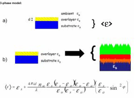
So far, we have assumed the ideal 3-phase case which is ambient-overlayer-substrate. However, in reality the actual phase is not mathematically abrupt 3 phase model since there are “interfaces” and “void” between each medium as shown in Fig. 1.6 [27,28].
two phases. K=2 assumes spherical microstructure.
In this study, two types of SE machines were used depending on the energy range of incident beam. One is visible-UV SE having an incident polarized beam generated by a xenon lamp with energy between 1.5 and 6 eV. This machine is working in ambient condition. The other machine is vacuum-UV SE covering higher energy range, from 4 to 10 eV, where deuterium UV lamp and 256-channeled Si based photomultiplier are used for a light source and detector. Also, the medium range vacuum (~ 10 mTorr) is maintained to minimize the scattered lights with particles in ambient at the higher energy above 6 eV. Both of SE machines are working in rotating compensator configuration [29].
1.6 Electrical techniques: Current-Voltage (I-V) and Capacitance-Voltage (C-V)
For electrical measurements, metal-electroded capacitors were fabricated using shadow masks on mid 1017 to low 1018 cm-2 n- and p-type Si and Ge substrate. Capacitors were prepared in class-100 cleanroom located at North Carolina State University (NCSU). The overall process steps include surface cleaning, sacrificial thermal oxide and high-k oxide growth, post deposition rapid thermal anneal (RTA), and dot metal electrode (Al) formation using evaporation. In the process included forming gas anneal (FGA) for 30 minutes in a mixture of 10% H2 in N2 at 400°C was used to minimize Dit. This step was done before metallization in order to prevent reactions between the Al gate metal and the dielectric films.
dispersion. Current-voltage measurements were done on an HP 4140B voltage source with a pico-ammeter. Voltage-ramp rates were varied from dV/dt = 0.001 V/sec to dV/dt = 0.05 V/sec. A slower ramp rate is preferred to reduce the displacement current, ensuring that the current measured is actually tunneling current. The temperature of the sample was maintained at 25°C and all measurements were performed in a light-tight box.
The focus on analysis on I-V measurements is to investigate the trap level’s role in injection and transport mechanism in leakage current process. This was possible from in-depth analysis of I-V traces based on the basic relation of possible transport mechanisms in oxides such as direct tunneling (DT), Poole-Frenkel (PF), trap assisted tunneling (TAT), and Folwer–Nordheim tunneling (FN) to the governing parameters such as temperature, trap depth, electric field, and dependence on trap density [30-32].
The focus on analysis on C-V measurements is to quantify trapped charges at defects in oxides. The specific methods for this are (i) trapped charge density extracted from C-V hysteresis and (ii) frequency dispersion of C-V traces giving information about dominant trap location (e. g. interface or bulk oxide region) [32,33].
1.7 Overview of dissertation
In order to achieve this goal, the main approach is a spectroscopic characterization on various TM/RE elemental/complex oxides in the context of thin films and correlation of those results to the electrical data on devices using the same oxides as gate dielectrics. However, analysis on data was not limited to the intrinsic properties of oxide itself but reached to the interfacial reaction to other materials such as substrate and metals. The main focus on this dissertation study is quantification of pre-existing defects from spectroscopic measurements and correlation of pre-existing defects to the trapped charges in device operation.
Chapter Two addresses the intrinsic bonding defects inherently existing in the nanocrystalline high-k dielectrics associated with the discrete asymmetric defect energy levels near the conduction and valence band edge. This study demonstrates the spectroscopic measurement techniques and analysis approaches to quantification of the defect density and energy states.
Chapter Three reports the relation of length scale of LaScO3 nanocrystalline to the conduction band changes driven by J-T distortion and localized defect behavior affected by grain growth with anneal and dimensional constraints
Chapter Four presents the pathway to suppress the pre-existing defects in BaSrTiO3 by Ni-doping. This study proves that doping of a proper metal into a perovskite oxide can successfully stabilize the local structure distortion and provide a enhancement of oxide reliability for device applications (i.e., metal-insulator-metal capacitor).
interfacial defects. The results propose the engineering solution for elimination of Ge-interfacial layers by post deposition anneal with thermally stable HfSiON.
Chapter Seven concludes the dissertation with a summary and suggestions for future work in these research areas.
1.8 References
[1] A. I. Kingon, J. P. Maria, and S. K. Streiffer, Nature 406, 1032 (2000).
[2] G. D. Wilk and R. M. Wallace, and J. M. Anthony, J. Appl. Phys. 87, 484 (2000).
[3]International Technology Roadmap for Semiconductor (2007 edn) at http://public.itrs.net. [4] D. A. Muller, T. Sorsch, S. Moccio, F. H. Buumann, K. Evans-Lutterodt, and G. Timp,
Nature 399, 758 (1999).
[5] M. Houssa, High-k Gate Dielectrics (Institute of Physics, London, 2004).
[6] G. D. Wilk, R.M. Wallace, and J.M. Anthony, Appl. Phys. Rev. 10, 5243 (2001).
[7] G. Lucovsky, J. Vac. Sci. Technol. A 19, 1553 (2001).
[8] R. Degraeve, N. Pangon, B. Kaczer, T. Nigam, G. Groeseneken, and A. Naem, IEEE Trans. Electron. Devices 45, 904 (1998).
[13] M. Houssa, L. Pantisano, L.-A°. Ragnarsson, R. Degraeve, T. Schram, G. Pourtois, S. De Gendt, G. Groeseneken, and M.M. Heyns, Mat. Sci. Eng. 51, 37 (2006)
[14] C. Carbal, C. Lavoie, A. S. Ozcan, R. S. Amos, V. Narayanan, E. P. Gusev, J. L. Jordan-Sweet, and J. M. E. Harper, J. Electrochem Soc. 151, 283 (2004).
[15] S. Zafar, V. Narayanan, A. Callegari, F. R. McFeely, P. Jamison, E. Gusev, C. Carbal, and R. Jammy, Symp. VLSI Technol. 44 (2005).
[16] G. Ribes, M. Rafik, and D. Roy, Microelec. Eng. 84, 1910 (2007).
[17] P. A. Cox, Transition Metal Oxides. Oxford, U.K.: Oxford Science, 1992.
[18] G. Bersuker, P. Zeutziff, G. Brown, and H. R. Huff, Materialstoday 7, 26 (2004).
[19] J. Robertson, J. Vac. Sci. Technol. B 18, 1785 (2000).
[20] G. Lucovsky, C. C. Fulton, Y. Zhang, Y. Zou, J. Luning, L. F. Edge, J. L. Whitten, R. J. Nemanich, H. Ade, D. G. Schlom, V. V. Afanase’v, A. Stesmans, S. Zollner, D. Triyoso, and B. R. Rogers, IEEE. Tran. Dev. Mat. 5, 65 (2005).
[21] P.A. Cox, The electronic Structure and Chemistry of Solids, U.K.: Oxford Science, 1987. [22] F. A. Cotton, Advanced Inorganic Chemistry, 3rd Edition (Interscience, New York, 1972). [23] Y. Zhang, Ph.D. thesis, North Carolina State University, 2005.
[24] H. A. Jahn and E. Teller, Proc. R. Soc. London A 161, 220 (1937).
[25] E. U. Condon and G. H. Shortley, The Theory of Atomic Spectra. Cambridge U.K.: Cambridge Univ. Press, ch. V, 1957,
[26] G. Lucovsky, J. G. Hong, C. C. Fulton, Y. Zou, R. J. Nemanich, and H. Ade, J. Vac. Sci. Technol. B 22, 1748 (2002).
Metrology for ULSI Technology: 2003 International Conference
[28] Irving P. Herman, Optical diagnosis for thin film processing, Academic process, 1996 [29] D. E. Aspnes and J. B. Theenten, J. Appl. Phys. 50, 4928 (1979)
[30] M. Houssa, M. Aoulaiche, S. De Gendt, G. Groeseneken, M.M. Heyns, A. Stesmans, Appl. Phys. Lett. 86 093506 (2005).
[31] T. Hori, Gate Dielectrics and MOS ULSIs, Springer-Verlag Newyork 1997. [32] S. M. Sze, J. App. Phys. 38, 2951 (1967).
[33] P. Masson, J. L. Autran, M. Houssa, X. Garros, and Ch. Leroux, App. Phys. Lett. 81,
non-crystalline SiO
2
free electron-like and
delocalized
Si 3s* + O 2p*
O 2p non-bonding
Si 3s,p + O 2p
π
Si 3s,p + O 2p
σ
~ 9 eV
5.7 eV
nano-crystalline ZrO
2
O 2p non-bonding
Zr 4d
π
+ O 2p
π
Zr 4d
σ
(5s,p) + O 2p
σ
Zr 5s*,p* + O 2p*
Zr 4d*
σ
(5s*,p*) + O 2p*
σ
Zr 4d*
π
+ O 2p*
π
significantly more
localized
d* states
optical band gap
non-crystalline SiO
2
free electron-like and
delocalized
Si 3s* + O 2p*
O 2p non-bonding
Si 3s,p + O 2p
π
Si 3s,p + O 2p
σ
~ 9 eV
5.7 eV
nano-crystalline ZrO
2
O 2p non-bonding
Zr 4d
π
+ O 2p
π
Zr 4d
σ
(5s,p) + O 2p
σ
Zr 5s*,p* + O 2p*
Zr 4d*
σ
(5s*,p*) + O 2p*
σ
Zr 4d*
π
+ O 2p*
π
significantly more
localized
d* states
5.7 eV
nano-crystalline ZrO
2
O 2p non-bonding
Zr 4d
π
+ O 2p
π
Zr 4d
σ
(5s,p) + O 2p
σ
Zr 5s*,p* + O 2p*
Zr 4d*
σ
(5s*,p*) + O 2p*
σ
Zr 4d*
π
+ O 2p*
π
significantly more
localized
d* states
5.7 eV
nano-crystalline ZrO
2
O 2p non-bonding
Zr 4d
π
+ O 2p
π
Zr 4d
σ
(5s,p) + O 2p
σ
Zr 5s*,p* + O 2p*
Zr 4d*
σ
(5s*,p*) + O 2p*
σ
Zr 4d*
π
+ O 2p*
π
significantly more
localized
d* states
5.7 eV
nano-crystalline ZrO
2
O 2p non-bonding
Zr 4d
π
+ O 2p
π
Zr 4d
σ
(5s,p) + O 2p
σ
Zr 5s*,p* + O 2p*
Zr 4d*
σ
(5s*,p*) + O 2p*
σ
Zr 4d*
π
+ O 2p*
π
significantly more
localized
d* states
nano-crystalline ZrO
2
O 2p non-bonding
Zr 4d
π
+ O 2p
π
Zr 4d
σ
(5s,p) + O 2p
σ
Zr 5s*,p* + O 2p*
Zr 4d*
σ
(5s*,p*) + O 2p*
σ
Zr 4d*
π
+ O 2p*
π
Zr 5s*,p* + O 2p*
Zr 4d*
σ
(5s*,p*) + O 2p*
σ
Zr 4d*
π
+ O 2p*
π
significantly more
localized
d* states
optical band gap
Fig 1.2. Schematic CB and VB band edge MO states in TiO2.
O 2p non-bonding
Zr 4d π+ O 2p π Zr 4d σ(5s,p) + O 2p σ
Zr 5s*,p* + O 2p*
Zr 4d* σ(5s*,p*) + O 2p* σ
Zr 4d* π+ O 2p* π
Valence band edge states Band edge states (O vacancy)
UPS, SXPS Valence band Conduction band
Energy
VUV SE (1.5 ~ 8.5 eV) transition from VBM to CB
Zr 3p (~ 340eV) Dipole allowed intra-atomic
transition
XAS OK1 edge
O 1s (~ 535eV) Inter-atomic transition
XAS ZrM2,3 edge
O 2p non-bonding
Zr 4d π+ O 2p π Zr 4d σ(5s,p) + O 2p σ
Zr 5s*,p* + O 2p*
Zr 4d* σ(5s*,p*) + O 2p* σ
Zr 4d* π+ O 2p* π Zr 5s*,p* + O 2p*
Zr 4d* σ(5s*,p*) + O 2p* σ
Zr 4d* π+ O 2p* π
Valence band edge states Band edge states (O vacancy)
UPS, SXPS Valence band Conduction band
Energy
VUV SE (1.5 ~ 8.5 eV) transition from VBM to CB
VUV SE (1.5 ~ 8.5 eV) transition from VBM to CB
Zr 3p (~ 340eV) Dipole allowed intra-atomic
transition
XAS OK1 edge
Zr 3p (~ 340eV) Dipole allowed intra-atomic
transition Zr 3p (~ 340eV) Dipole allowed intra-atomic
transition
XAS OK1 edge
O 1s (~ 535eV) Inter-atomic transition
XAS ZrM2,3 edge
O 1s (~ 535eV) Inter-atomic transition
O 1s (~ 535eV) Inter-atomic transition
XAS ZrM2,3 edge
2 Spectroscopic Defection of Defects present in TM/RE
Elemental/Complex High-k oxides
Abstract
2.1 Introduction
The densities of interfacial and bulk traps, and fixed interfacial charge in complementary metal–oxide–semiconductor (CMOS) devices with high-k dielectrics are typically about two orders of magnitude higher (~1012cm-2) than those in Si–SiO
2 devices [1]. A crucial issue is whether these high-k oxide defects are intrinsic and associated with bonding on a particular nanocrystalline length scale, or whether they are derived from chemical impurities introduced during processing. These bonding defects have been confirmed as electrically active defects which are asymmetry trapping sources for holes and electrons. Many reports revealed that trapping kinetics in high-k dielectric gate stacks represent a potentially significant limitation for the operation and reliability of Si CMOS devices and circuits [2,3].
Although many studies on defects in high-k dielectrics have employed theoretical calculations such as local density approximation (LDA) and density functional theory (DFT), the energy location and charge status of defects (i.e., oxygen vacancies and interstitials) deviated from the experimentally observed results which might be due to the incorrect basis set ignoring the severe local distortion driven defect formation [4,5].
The Si, Hf/Ti source gases, 2% SiH4 in He, and Hf (IV)/Ti (IV) t-butoxide respectively, were delivered directly into the substrate region of a remote plasma reactor through two different injectors. An N2/N2O/He mixture was subjected to remote plasma excitation at 30 W and 13.56 MHz and was used to initiate RPECVD process. Prior to the Hf/Ti oxynitride-alloy deposition, a thin nitridation layer approximately 0.6 nm thick was deposited on the Si substrate by RPECVD to provide chemical passivation to suppress further unwanted reaction between the deposited Hf/Ti Si oxynitride alloys and the Si substrate. Upon deposition, heat treatment of samples was done by rapid thermal annealing (RTA) at 900 and 1100 °C.
Soft X-ray photoelectron spectroscopy (SXPS on beam-line U4A at the National Synchrotron Light Source), near edge X-ray absorption spectroscopy (NEXAS on beam line 10-1 at the Stanford Synchrotron Research Laboratory), and visible- and vacuum ultra-violet spectroscopic ellipsometry (VUV SE) have been performed on nano-crystalline transition metal (TM) elemental/complex oxides.
2.3 Results and Discussion
Two sub-sections on TM (i) elemental and (ii) complex oxides will be addressed here.
2.3.1 Defects in TiO2 and HfO2
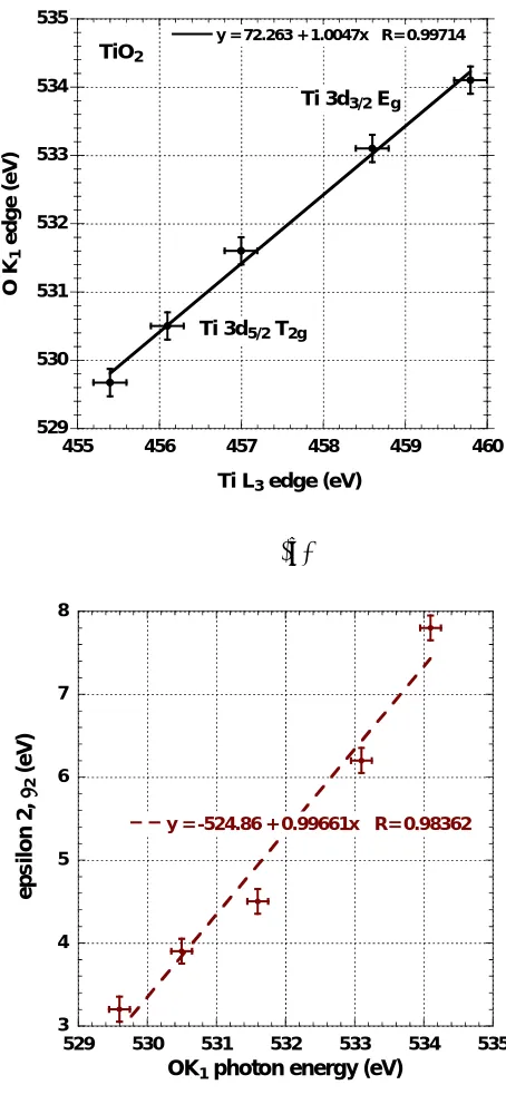
The J–T energy differences for the T2g and Eg states are 0.7 ± 0.2 eV, which are smaller by about a factor of about four than the average C-F splitting. The linearity of the relationship in Fig. 2.2 (a), particularly the slope at ~1 supports this interpretation in terms of C-F and J–T splittings.
Figures 2.3 (a) and (b) respectively display the epsilon 2 (ε2) spectrum for TiO2, obtained by i) the analysis of VUV-SE measurements and ii) the valence band spectrum for TiO2 by the analysis soft X-ray photoelectron spectroscopy (SXPS) measurements. The d-states have been extracted from the minima in the second derivative of the ε2 spectrum, and their relative energies in Fig. 2.2(b) are compared with those of the d-state features obtained from the differentiation of the O K1 spectrum. This plot is also linear with a slope ~1, the same slope as in Fig. 2.2(a). However, the equally important SXPS valence and ε2 conduction band edge spectra in Figs. 2.3(b) and 2.3(a), respectively, show additional spectral features as (i) a doublet structure at the valence band edge and (ii) a broad spectral feature at the conduction band edge. These are respectively attributed to the occupied bonding and unoccupied anti-bonding states of intrinsic bonding defects associated with an O-deficient TiO2 stoichiometry, TiO2-δ [6]. For TiO2, these defect states are consistent with the electronic states of Ti3+ atomic species associated with local Ti
2O3 bonding, or equivalently O-atom vacancies at the grain boundaries of these nanocrystalline films [6-8].
valence band edge. Comparing to SXPS spectra of TiO2, the higher lying valence band edge defect state and broad defect state feature below the conduction band edge are at essentially the same energy relative to the valence band edge, ~2.3 0.2 eV, suggesting that they are associated with a partially occupied state of the same bonding defect.
From those spectroscopic measurements on HfO2 and TiO2, the model on band edge and pre-existing paired defect states are suggested in Fig 2.5 (a) and (b) respectively. Similarly to other calculation models on defect states in HfO2, spectroscopically resolved defect states are indeed discrete and paired. Nevertheless, those calculations have inherent limitation in explaining the origin of defects by using incorrect wave basis sets and generating hypothetical combination of oxygen vacancies and interstitials which will be subject to the serious recombination in a real situation.
In contrast, our model constructed from spectroscopic measurements explains the origin of defects with molecular orbital states of oxygen deficient Ti3+ or Hf3+ in sub-oxides in stoichiometric TiO2 or HfO2. Therefore, it can be quantified by describing O-deficient TiO2-δ
thermal stability of high-k dielectrics using pseudo-ternary alloys. The stability of high-Si3N4 content TM Si oxynitride alloys, (SiO2)x(Si3N4)y(Ti/Zr/HfO2)1-x-y, against a chemical phase separation (CPS) has been established by spectroscopic studies [7,9,10]. TM Si oxynitride alloys were deposited at 300 °C by RPECVD and annealed in Ar at temperatures up to 1100
°C. The alloys with approximately equal SiO
Consistent with the corresponding behavior of TiO2 noted above, the spectra in Fig. 2.6 also establish that the d-state features in the O K1 spectrum terminated in the same anti-bonding d-states as in ε2 spectra. However, it should be noted that each spectrum also displays a significant tailing of states into the forbidden band gap suggestive of intrinsic defects associated with the inherent noncrystallinity of these films. Since these states are energies less than 5.5 eV, they may be associated with the Si–N bonding of these alloys, and in particular band-tail defects localized on the nitrogen atoms.[13]
Figure 2.7 represents the similar ε2 spectra of Hf-Si oxynitride showing the strong dependence of thermal stability onto Si3N4 composition ratios. Although differences in spectral features before and after an annealing are not severe as in Ti-Si oxynitride, lower Si3N4 content alloys revealed the additional states at about 6.5 eV and more pronounced edge states which might be partially due to CPS driven local bonding defects. In contrast, there are no noticeable spectra changes in 40% Si3N4 alloy both for edge and higher energy states in ε2 spectra. The much softer edge of ε2 spectra in 40% Si3N4 alloy indicates its non-crystalline character, and this was confirmed in a previous XPS study on Zr-Si oxynitrides revealing no changes in oxygen bonding states before and after anneal [10].
SiO2 and the TM elemental oxide, e.g., ZrO2 [14]. Alloys with Cav in the range between 2.9 and 3.2 generally form intermediate phases in which defects and defect precursors are minimized making them ideal candidates for device applications. Cav increases modestly to ~3.15 when the Si3N4 concentration is increased to 40%, and the SiO2 and TM elemental oxide concentrations are reduced proportionally to ~30%. This higher Si3N4 content creates regions of local rigidity associated with the Si3N4 alloy fraction being greater than the SiO2 fraction. However, this local rigidity cannot percolate throughout the sample, and does not change the intermediate phase properties of these alloys. The bonding arrangements in these alloys results from a chemical boding self-organization that optimizes bonding properties, reducing configurational entropy associated with random bonding, but reducing bond strain to compensate for the entropy reduction.
2.4 Summary
The spectroscopic data in this paper have indicated that: (i) defect state features are at the valence band edge in TiO2 and HfO2 as determined by SXPS and below the conduction band edge as determined by NEXAS, vis–VUV SE, and (ii) on the basis of the results of comparisons with intrinsic d-state features, these defect state densities can be >1013 cm-2 [or equivalently > (3 - 5)× 1019 cm-3]; (iii) defect states in HfO
supported by the results of studies on noncrystalline group IVB TM Si oxynitrides; and finally (vi) even though discrete Ti3+and Hf3+ valence and conduction band edge defects have not been observed in thin film dielectrics identified in (vii), these dielectrics show band edge tailing, indicative of pre-existing defects at order of magnitude lower concentrations than the grain-boundary-associated defect densities in the nanocrystalline.
2.5 References
[1] J. L. Autron, D. Munteanu, and M. Houssa, in High-k Gate Dielectrics, ed. M. Houssa (IOP Publishing, Bristol, 2004) Chap. 3.4.
[2] M. Houssa, M. Naili, C. Zhao, H. Bender, M. M. Hyens, and A. Stesmans, Semicond. Sci. Technol. 16, 31 (2001).
[3] Z. Xu, M. Houssa, S. DeGendt, and M. Hyens, Appl. Phys. Lett. 80, 1975 (2002).
[4] K. Xiong, J. Robertson, M. C. Gibson, and S. J. Clark, Appl. Phys. Lett. 87, 183505
(2005).
[5] A. S. Foster, F. Lopez Gejo, A. L. Shluger, and R. M. Nieminen, Phys. Rev. B 65, 174117
(2002).
[9] G. Lucovsky and J. Lu¨ning, Proc. ESSDERC 2005 p. 439. [10] B. Ju, Dr. Thesis, NC State University, Raleigh, U.S.A. (2003).
[11] G. B. Rayner, D. Kang, and G. Lucovsky, J. Vac. Sci. Technol. B 21, 1783 (2003).
[12] J. P. Maria, D. Wickanana, P. Parrette, and A. I. Kingon, J. Mater. Res. 17,1571 (2002).
[13] M. J. Williams, S. M. Cho, S. S. He, and G. Lucovsky, J. Non-Cryst.Solids 164, 67
(1993).
(a) 0.15 0.2 0.25 0.3 0.35
525 530 535 540 545 550
a b s o rp tion (a rb . un it s)
X-ray photon energy (eV) O K1 TiO2
T2g(3) Eg(2) A1g T1u 3d5/2π* 3d3/2σ* 4s σ* 4p σ*
0.2 0.3 0.4 0.5 0.6 0.7 0.8
Ti L3 TiO2 absorptio n (arb . un its) 3d5/2
T2g(3)
π*
3d3/2 Eg(3)
(a)
(b)
Fig. 2.2. Photon energies of Ti d-state features: (a) O K1 edge vs Ti L3 edge and (b) ε2 vs O K edge.
529 530 531 532 533 534 535
455 456 457 458 459 460
y = 72.263 + 1.0047x R= 0.99714
O K
1
edge
(eV)
Ti L3 edge (eV)
Ti 3d5/2 T2g
Ti 3d3/2 Eg
TiO2
3 4 5 6 7 8
529 530 531 532 533 534 535
y = -524.86 + 0.99661x R= 0.98362
eps
ilon 2,
ε2
(eV)
(a)
0.1 1 10
2 3 4 5 6 7 8
photon enegy (eV)
TiO2 - VUV SE
S Zollner, D Tryoso T2g Eg
TiO2 expsilon 2 defect states im agi n ary par
t of di
elec tric c o ns tant ( ε2 ) 1000 104 photo e lectron c o unts
6 σ - bonds
3d3/2 4p 4s
Eg
3d5/2 T2g 3 π bonds
(a)
(b)
Fig. 2.4. (a) SXPS VB structure versus binding energy and (b) VUV SE ε2 spectrum versus photon energy for HfO .
5 6 7 8
104
105 106
2nd Eg
Absorption c o e fficient (c m -1 )
Photon energy (eV)
PVD HfO
2 (30 nm) 900°C annealed
Hf3+ defects
1st Eg
∆E
g ~ 1.4 eV
1000 104
0 2 4 6 8 10 12 14 16
binding energy (eV) 2
π
-bonds5d3/2 Eg pho toel ectr on c ounts SXPS VB 60 eV HfO2 defect states
7
σ
-bonds 5d3(a) 0 1 2 3 4 n er g y r e la ti ve t o v a le n c e ba nd e d g e (e V)
TiO2 valence band TiO2 conduction band
SXPS
VUV SE
Ti3+ T
2g states XAS
VUV SE XAS VUV SE -1 0 1 2 3 4 5 6 7 ene rgy (e V )
local density of states HfO2 conduction band
Fig. 2.6. O K1 and ε2 spectra for low and high Si3N4 content Ti Si oxynitride alloys. 0.16
0.18 0.2 0.22 0.24 0.26 0.28 0.3 0.32
526 528 530 532 534
O K1 Ti SiON
900oC
ε2 Ti SiON
900oC
+ 522.8 eV 4-fold coord.
1.7 eV
2.6 eV
6-fold coord.
R(∆Ed) = 1.53 ~ 6/4 16% Si3N4
40% Si3N4 40% Si3N4
x-ray photon energy (eV)
absorption,
e2
(arb
(a)
4 5 6 7 8 9
0 1 2 3 4 5
Annealed
e2
Photon energy (eV)
e2 (as dep - VUV: 100A) e2 (annealed - VUV: 99A)
20% Si
3N
4As-deposited
1 2 3 4 5
e2
e2 (as dep - VUV: 96A) e2 (annealed - VUV: 96A)
N
Si
O
Zr
N
Si
O
Zr
cavity
N
Si
O
Zr
N
Si
O
Zr
cavity
N
Si
O
Zr
N
Si
O
Zr
cavity
3 Correlation of Length Scale of TM/RE Oxides and Interfaces to
Intrinsic Defects
Abstract
This paper uses (i) spectroscopic measurements; X-ray absorption and vacuum ultra-violet spectroscopic ellipsometry, (ii) high resolution transmission electron microscope, and (iii) internal photoemission spectroscopy to distinguish between non-crystallinity, and the suppression of Jahn-Teller splittings that identify a scale of order metric, λs, of ~3 nm for distinguishing between i) nanocrystalline-order that can be detected by x-ray diffraction for
λs > 3-4 nm, and ii) reduced nanocrystalline order that can be detected by atomic-scale
imaging and extended X-ray absorption spectroscopy for λs < ~2.5 nm. The coherent π
-bonding coupling is strongly associated to J-T split driven localized oxygen -bonding defects
at grain boundary in LaScO3 and the incoherent π-bonding coupling is related to oxygen
3. 1. Introduction
There has been much debate and interest in the possible existence of a non-crystalline phase for transition metal (TM) and rare earth (RE) atom elemental and complex oxides. TM and RE silicates, and TM Si oxynitride alloys can be deposited as noncrystalline thin films; however, this does not apply to elemental and complex TM and RE atom elemental and complex oxides having fairly high dielectric constants. The absence of line features in conventional X-ray diffraction (XRD) measurements has often been used to label a material as being X-ray amorphous, a designation which lacks any substance. In marked contrast, this paper uses X-ray absorption and vacuum ultra-violet spectroscopic ellipsometry (VUV-SE) to distinguish between noncrystallinity, and the suppression of Jahn-Teller (J-T) splittings that identify a scale of order of ~3 nm for distinguishing between two distinct and different regimes of nanocrystallinity: i) nanocrystalline order that can also be detected by X-ray diffraction for λs > 3-4 nm, ii) reduced nanocrystalline order that can only be detected by atomic-scale high resolution transmission electron microscope imaging (HRTEM) and extended X-ray absorption spectroscopy (EXAFS) for λs < ~2.5 nm [1,2], and iii) finally physical correlation of empty energy state changes of J-T driven intrinsic d-states and localized defects to the length scale of order in oxides.
3. 2. Experimental Procedures
before the film deposition. Deposited samples were respectively annealed for 1 min from 700 to 1000 °C in an inert ambient. The film thickness analyzed by SE is about 40nm. Films were studied by HRTEM (UCSB), VUV SE and X-ray absorption spectroscopy (XAS). MOS capacitors consisting of transparent Ag electrodes/LaScO3/Si were fabricated for internal photoemission spectroscopy (IPS) measurements at KU Leuven and photoconductivity (PC) spectra under the voltage bias were measured with the exposure of UV light swept from 1.5 and 6 eV.
XAS and SE spectra have also been obtained for 0.38 nm LaAlO3 films on single crystal SrTiO3.[2] These were prepared by reactive sputtering. XAS measurements were made the Stanford Synchrotron Research Laboratory (SSRL).
3.3 Results and Discussion
the distorted bonding environments, the degeneracy of constituent atom valence and conduction band d-states with spherical symmetry is removed [5]. Therefore, as the structure evolves from symmetric structure to distorted one, a distinction between i) J-T term splittings and ii) C-F splitting can be a clear reference to determine either symmetric bonding environment or asymmetric one with localized bonding distortion.
Figure 3.4 displays the evolution of C-F and J-T term splitting for TiO2 d-states from i) a regular octahedral and then to ii) distorted octahedral and finally to iii) additional distortions that occur at grain boundaries in nanocrystalline films. LaScO3 has the same octahedral bonding environment as TiO2 so that the evolution of LaScO3 d-state splittings is almost same as TiO2 but with a slight difference in energy of term-splittings. From ab initio calculation guided by molecular orbital (MO) theory, the three lower states and two higher states have been assigned as T2g in π anti-bonding characteristic and Eg in σ anti-bonding characteristic respectively [6]. The J-T term splitting becomes larger as bonding environments are subject to more aggressive distortions and therefore decreases the conduction edge level to the lower energy. The physical reason for the presence of J-T distortion in TM/RE oxides has been regarded as the electrostatic stabilization of localized metal-oxygen bondings [5].
annealed at 700 °C and 1000 °C. The change of d-states also reveals the overall energy shift of T2g states to the lower energy in Sc L2,3 edge spectra and the significant change of edge states in O K1 spectra. In Fig. 3.1 (b), The T2g term splitting are 0.8±0.5 eV, and the average T2g-Eg is about 2.7 eV. This term-splitting is approximately the same as the Ti L3 edge spectra for TiO2 thin film which has the same local bonding environment as LaScO3, i.e., 6-fold octahedral Ti-O bonding [6]. XRD studies have detected crystallinity after an 850°C anneal, but not in as-deposited or 700°C annealed samples. This implies that the XAS spectra are more sensitive to nanocrystalline films than XRD [8]. Since XRD can detect the nano-crystallites at a scale greater than 4 nm but can not distinguish between i) amorphous films, and ii) nanocrystalline films with grain size smaller than 4 nm, as-deposited and 700°C annealed thin films are considered to have the 1 ~ 2 nm nano-crystallites.