ABSTRACT
BIGGERSTAFF, TRINITY LEIGH. Characterization of the Origin of Mobility Loss at the SiC/SiO2 Interface. (Under the direction of Dr. Gerd Duscher).
Silicon carbide (SiC) is a wide band gap semiconductor with material properties which make it ideally suited for high temperature, high frequency, and high power metal oxide semiconductor field effect transistor (MOSFET) applications. The wide scale commercial development of these devices has been hindered due to disappointing electron mobility when compared to properties of the bulk material. This mobility loss has been associated with the interface between SiC and the native oxide formed (SiO2). Many improvements in mobility have been realized, but it is currently still significantly less than that of the bulk material. The work in this dissertation is aimed at understanding the origin of this mobility loss from an atomic perspective.
interface, causing a carbon pileup on the SiC side of the interface, which we detect as a transition region. The rate of oxidation is also very important as oxidizing at a fast rate leads to greater carbon pileup. The extra carbon in this transition region acts as electron scattering centers, which ultimately lead to a reduced electron mobility.
Atomic Scale Characterization of the Origin of Mobility Loss at the SiC/SiO2 Interface.
by
Trinity Leigh Biggerstaff
A dissertation submitted to the Graduate Faculty of North Carolina State University
In partial fulfillment of the Requirements for the degree of
Doctor of Philosophy
Materials Science and Engineering
Raleigh, North Carolina October, 31 2008
APPROVED BY:
_______________________________ ______________________________
Dr. Gerd Duscher Dr. Lewis Reynolds
Committee Chair
DEDICATION
BIOGRAPHY
Trinity Leigh Biggerstaff was born and raised in Vale, North Carolina. She attended
Fred T. Foard High School in Newton, NC. After high school, she enrolled at North Carolina
State University in the college of engineering, where she ultimately went on to join the
Materials Science and Engineering Department and obtain a Bachelor of Science in Materials
Science and Engineering in 2005.
During her undergraduate studies, Trinity joined the research group of Dr. Gerd
Duscher and this ultimately led to her decision to pursue a graduate career in this group.
After completing her Bachelor of Science, she enrolled in North Carolina State University as
a graduate student and her PhD research focused on using analytical electron microscopy to
determine the origins of mobility loss at the SiC/SiO2 interface. In addition to her research,
during graduate school, Trinity worked in the Atomic Resolution Electron Microscopy
Facility (AREMC) as a teaching assistant for 3 years. She earned a Masters of Materials
Science and Engineering in May of 2007.
ACKNOWLEDGEMENTS
There are lots of people who helped me along the way who I would like to acknowledge. First, Dr. Gerd Duscher for providing the opportunity for me to work in his
group, encouraging me to pursue a PhD, and helping me to gain confidence as a researcher. I
would not have been able to complete my degree without the countless hours of one-on-one
training and help with equipment, as well as his availability for technical discussions. I fully
recognize his important role in my graduate work and I am extremely grateful. Dr. Lewis
Reynolds has also been very helpful to me with analysis of electrical data, as well as personal
encouragement, and advice. I am also grateful to the other members of my committee, as
their role is also critical: Dr. Nadia El Masry, and Dr. Salah Bedair.
I could not have been able complete my experiments without the use of the Atomic
Resolution Electron Microscopy Facility at N. C. State. This facility is great due to the
commitment and expertise of Dr. Thomas Rawdanowicz. Thank you Tom, for working so
hard to keep the TEMs working at a world class level, and thank you for mentoring my
teaching and ultimately helping me to become a better microscopist.
My research would not have been possible without funding from the Army Research
Laboratory (ARL) and Cree, Inc. I am very grateful to Dr. Tsvetanka Zheleva, and Aivars
Lelis at ARL, and to Dr. Anant Agarwal, Dr. Sei-Hyung Ryu, Dr. Sarit Dhar, and Sarah
also like to acknowledge Dr. Wolfgang Windl at Ohio State University and Dr. Sanwu Wang
at the University of Oklahoma at Tulsa for their valuable help with theoretical calculations
based on our experimental data.
The members of Dr. Duscher’s research group, past and present, have also been very
important to my success as a graduate student. I am very thankful to my senior group
members, Dr. Donovan Leonard, Dr. Fude Liu, Dr. Lirong Pei, and Dr. Wenjun Zhao for
helping to train me in electron microscopy. Also, Siddhartha Mal and Xiangyu Yang for
helping me with data analysis, and especially to Ryan McClellan for all of his sample
preparation and data analysis help.
Finally, I am most thankful for my friends and family. There are no words to describe
the amount of support and encouragement I have had from all of you, and I sincerely
TABLE OF CONTENTS
LIST OF TABLES………. ix
LIST OF FIGURES……… x
Chapter 1: Literature Review ……… 1
1.1 Silicon Carbide Semiconductor Properties ………. 1
1.2 Physics of Silicon Carbide ……….. 7
1.2.1 Crystal Field and Blocking Voltage ………. 7
1.3 Technology Status and Challenges ………. 9
1.3.1 SiC Wafer Quality ……… 10
1.3.2 Gate Oxide ………... 12
1.4 The SiC/SiO2 Interface ………... 14
1.4.1 Scattering Mechanisms ………... 14
1.4.2 Interface Defects ………. 16
1.4.3 Interface Passivation ………... 21
1.5 Process Optimization ………. 28
1.5.1 Channel Implantation ……….. 28
1.5.2 Gate Oxide Growth ………. 29
1.5.3 NO Annealing ………. 29
1.6 MOSFET Introduction ………... 31
2.1 Z-contrast Imaging with a Scanning Transmission Electron Microscope … 34
2.2 Atomic Resolution Electron Energy Loss Spectroscopy (EELS) ………….. 37
2.2.1 Qualitative Compositional Analysis ………... 40
2.2.2 Quantitative Compositional Analysis ………. 42
2.2.3 Energy-Loss Near-Edge Fine Structure (ELNES) ……….. 44
2.2.4 Dept Profiling ………... 46
2.3 Theory of Convergent Beam Electron Diffraction (CBED) ……….. 47
2.3.1 Introduction to CBED ………. 47
2.4 Transmission Electron Microscopy (TEM) Sample Preparation ………...… 49
2.4.1 Conventional Sandwich/Ion Milling Sample Preparation ……...… 50
2.4.2 Focused Ion Beam (FIB) Sample Preparation ………. 52
Chapter 3: Results and Discussion ………... 54
3.1 Effect of Processing Conditions on Microstructure .……….. 54
3.1.1 Carbon Rich Transition Region ……….. 55
3.1.1.2 Sample 21 ……… 55
3.1.1.3 Sample 21B ………. 59
3.1.1.4 Sample 9 ……….. 63
3.1.1.5 Sample 9B ………... 65
3.1.1.6 Standard Oxide ………... 69
3.1.1.7 Qualitative Estimation of the Oxidation Rate ………… 72
3.2 Linear Relationship ………... 74
3.3 Tilt ………. 76
3.3.2 Low Angle Grain Boundary ………... 82
3.4 Scattering Length and Physical Parameters Affecting Mobility …………... 83
3.5 The “Snowplow” Effect ……….. 87
3.6 Varying Annealing Temperature ……….… 93
3.6.1 Z-Contrast Images of the Interface ……….….. 95
3.6.2 Low Angle Dark Field Imaging of the Interface ……….…. 99
3.6.3 Electron Energy Loss Spectroscopy Results from A,B,C,D ……. 102
3.7 Backside of the Wafer ……….. 110
3.8 Discussion ………. 111
3.9 Future Prospects ……… 115
LIST OF TABLES
Table 1-1: Critical materials values in 4-H SiC and Si ……… 2
Table 3-1: Processing conditions and descriptions of samples received from Army
Research Laboratory ………... 55
Table 3-2 Transition layer width and mobility data for samples studied ……….. 75
Table 3-3 Tilt in degrees between the transition layer and bulk SiC for each sample . 79
Table 3-4 calculated τ and l values from samples with measurable mobility data …… 84 Table 3-5 Calculations based on mobility and EELS data ……….. 86
LIST OF FIGURES
Figure 1-1: (a) The basic structural building block of the SiC system is the Si-C tetrahedron which consists of one silicon atom which is bonded to four carbon atoms. (b) A close packed hexagonal sheet of atoms with the centers at position A. An identical sheet of atoms can be stacked on top of this sheet with centers at position B or C………1
Figure 1-2: Bandgap and relative band offsets of several common SiC polytypes, SiO2, and Si. Information in figure is compiled from results by Afanas ev et al ...…………. 4
Figure 1-3: Hexagonal unit cell indicating commonly used faces. Relative C and Si contents are indicated……….. 5
Figure 1-4: Oxide thickness over time for 3 different faces of 4H-SiC. Si is shown as reference. Values are measured by ellipsometry (filled symbols) or Rutherford Scattering (empty symbols)……….. 6
Figure 1-5: Schematic of the density of traps at the oxide/semiconductor interface. The relative positions of the conduction band (Ec) and valence band (Ev) edges are indicated. 4H-SiC is sensitive to a larger amount of states than 6H-SiC and silicon. This illustration is modified from a publication by Schorner et al………..17
Figure 1-6: Dit obtained by CV (shown above as triangles) and conductance (shown above as circles) measurements as a function of the energy within the band-gap of 6H-SiC (filled symbols) and 4-H SiC (empty symbols). The Dit at oxide interface formed on the Si-face of the two polytypes are similar throughout the gap and rises sharply between their conduction band edges ……….19
Figure 1-7: Defects which can occur at the SiC/SiO2 interface and their respective energy levels in the 4H-SiC band-gap. From Pantelides et al ……..……… 21
Figure 1-8: Interface trap densities in the upper half of the 4H-SiC band-gap obtained after different post-oxidation anneals. Discontinuities near Ec-E~0.6eV are the result of CV measurements taken at 23oC and 300oC, to extract D
Figure 1-9: Improved channel mobilities extracted from MOSFETs fabricated on different faces of 4H-SiC. The Si-face mobility prior to NO annealing is shown as a reference ………. 24
Figure 1-10: Achievable specific ON resistance as a function of the designed blocking voltage for Si and 4H-SiC devices. Continuous lines indicate the theoretical limits set by the drift the drift resistance alone. Dotted lines indicate the impact of the channel resistance on the total resistance for a poor (as-oxidized) and a better (NO-annealed) interface. The symbols correspond to values extracted from actual SiC MOSFETs
fabricated before105,106,107(shown above as triangles) and after108,109,110,111 (shown
above as squares) 2001. Note, figure adapted from Rozen ………...30
Figure 1-11: Vertical DIMOSFET. Left: n-inversion channel formed by the application of a positive gate voltage VG. Right: conducting inversion channel does not form when VG is removed. Inset: Interfacial defects arising from Si-Si bonds, C-C bonds, Si dangling bonds and missing O atoms ………...………. 32
Figure 2-1: a)schematic of the STEM b) the experimental image can be interpreted as a simple convolution of the experimental probe and the object function ………35
Figure 2-2: A typical EELS spectra ………. 38
Figure 2-3 EELS linescan across the Si/SiO2 interface indicating a 6 eV shift in the L3,2 edge onset ……….……….. 41
Figure 2-4: Experimental and theoretical X-ray absorption spectra of the Si-L2,3 edge. There is a close match between the two thick black curves which are from “experiment” (top) and “core-hole”—full calculation including electron-hole interactions (bottom). The two thin black curves are from “Z+1” model (left) and “Z”—calculation without electron-hole interactions (right) ……… 46
Figure 2-5 Ray diagrams indicate (a) parallel illumination forms a spot pattern in the selected area diffraction setup; (b) converged illumination forms a disc pattern in convergent beam electron diffraction setup ………..… 48
Figure 2-7 The correlation between the thickness of the sample and the corresponding Nomarski fringes present ………...……… 52
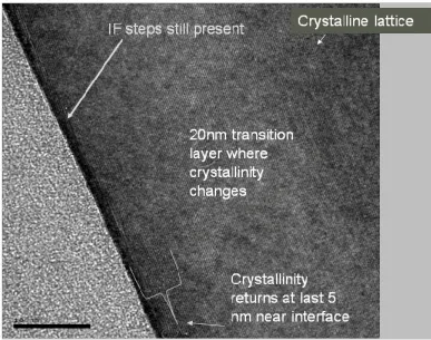
Figure 3-1 Z-Contrast image and corresponding intensity profile (inset) from indicated area from sample 21 ………..……… 58
Figure 3-2 Atomic Ratios calculated with EELS data corresponding to the indicated areas of sample 21. The ratios indicate a carbon rich transition region on the SiC side of the
interface………... 59
Figure 3-3 HRTEM image of sample 21B indicating microstructure consistent with a buried implantation layer ……….. 61
Figure 3-4 Z-contrast image and corresponding intensity profile of sample 21B used for quantitative measurement of 25nm total transition layer width ……… 62
Figure 3-5 Atomic ratios calculated from EELS spectra corresponding to interface region of sample 21B indicating a carbon rich transition region ……….. 63
Figure 3-6 Z-contrast image and corresponding intensity profile of indicated area used to quantitatively measure width of the 6nm transition region in sample 9 ……… 65
Figure 3-7 Atomic ratios calculated from EELS spectra corresponding to interface region of sample 9 indicating a carbon rich transition region ……….. 66
Figure 3-8 Z-contrast image and corresponding intensity profile of indicated area used to quantitatively measure width of the 11 nm transition region in sample 9B ………. 68
Figure 3-9 Atomic ratios calculated from EELS spectra corresponding to interface region of sample 9B indicating a carbon rich transition region ……… 69
Figure 3-10 Z-contrast image and corresponding intensity profile of indicated area used to quantitatively measure width of the 8 nm transition region in Cree’s standard oxide sample ………...………. 71
Figure 3-11 Atomic ratios calculated from EELS spectra corresponding to interface region of Cree’s standard oxide sample indicating a carbon rich transition region …………. 72
Figure 3-12 Plot of the transition layer thickness versus mobility indicating linear
Figure 3-13 Convergent beam electron diffraction (CBED) patterns of sample 9 taken from (a) bulk SiC and (b) transition region. The red rectangle represents the center of the pattern to illustrate the clear tilt associated with the transition region ……….77
Figure 3-14 CBED data collected from (a) sample 21B bulk SiC; (b) sample 21B transition layer; (c) sample 9B bulk SiC; (d) sample 9B transition layer; (e) sample 21 bulk SiC; (f) sample 21 transition layer; (g) Cree standard oxide sample bulk SiC; (h) Cree standard oxide transition layer. The red rectangle on each CBED pattern indicates the center of the pattern to illustrate the tilt ……… 81
Figure 3-15 Schematic of possible low angle grain boundary assoicated with transition
region……….. 83
Figure 3-16 Plot showing linear relationship between distance between excess carbon and mobility scattering length ……….. 86
Figure 3-17: Z-Contrast image of conventional sample with corresponding atomic ratios as calculated from EELS results ………. 88
Figure 3-18: (a) Atomic ratios in sample calculated based on EELS data indicating the region selected for fitting and (b) the fitted region from (a) ………. 92
Figure 3-19 Characteristic interface images from samples A, B, C, and D indicating the presence of steps at the interface and the tendency of these steps to bunch. (a) indicates an area of the interface with few steps while (b) shows many more steps in the same amount of area as (a). Both samples are oriented in the 1120] zone axis.96 Figure 3-20 Z-contrast images of sample (a) A, (b) B, (c) C, and (d) D. These images show
a chemically abrupt interface with steps at the interface. There are no significant differences in the interface of the samples. All images are taken in the 1120 zone
axis ………. 97
Figure 3-22 Background Subtracted plots of sample B of interface and adjacent spectra, the linear combination model, and the difference between the two in the silicon region. Background subtractions were performed using QuantiFit ………...…...105
Figure 3-23 Background subtracted plots of sample B of interface and adjacent spectra, the linear combination model, and the difference between the two in the oxygen region. Background subtractions were performed using QuantiFit ………..…... 106
Figure 3-24 Background subtracted plots of spectra collected at and adjacent to the interface in the carbon region. Background subtraction performed using QuantiFit ……... 108
Figure 3-25: Background subtracted carbon peaks from the 2nd monolayer of each of the samples A, B, C, and D, as well as a characteristic carbon peak for SiC for comparison. The peaks from each of the four samples were basically the same with the only noticable differences being in the noise level. Background subtractions performed using QuantiFit ………..………. 109
Figure 3-26 Z-contrast image of carbon face of wafer A showing a transition region which is a result of a rapid oxidation rate ……… 99
Figure 3-27 Schematic illustrating potential implications of combining slow oxidation rate with NO annealing ………... 115
CHAPTER 1: LITERATURE REVIEW
1.1 Silicon Carbide Semiconductor properties
Silicon carbide is the only compound of silicon and carbon which is currently known. The
following sections review the properties of SiC as well as recent advancements in the
technology. It can exist under various structures called polytypes1 with a common building
block, the Si-C tetrahedron. This tetrahedron can be seen in figure 1-1 (a) (adapted from ref
1). This structure consists of one silicon atom bonded to four carbon atoms or conversely,
one carbon atom bonded to four silicon atoms.
The Si-C bond length in SiC is 1.89 Å which is smaller than the 2.35 Å bond length for the
Si-Si system which indicates that there is a stronger atomic interaction in the SiC system.
Based on this, it is expected that SiC is a stiffer material than silicon, which is confirmed by
the higher Young’s modulus. Table 1-1 indicates some critical materials values in 4-H SiC
and Si.
In addition to the Youngs modulus, it is important to note that due to the fact that carbon is a
significantly lighter atom than silicon, which promotes lattice vibrations and ultimately leads
to SiC having a much higher thermal conductivity than that of silicon.
Each of the SiC polytypes is constructed by stacking a close packed planar hexagonal
array of the Si-C tetrahedra joined at the corners. This can be seen in figure 1-1(b). After the
addition of each tetrahedra plane, the upper tetrahedra can be aligned between the bottom
ones in two different ways. In figure 1-1B, if A is used as the reference point, then B and C
represent the two possible positions of the upper tetrahedra. It is also important to note that
the tetrahedra can be rotated 180o along the stacking direction, leading to planes labeled A’,
B’, and C’. While there are some rules restricting the stacking of the planes, it is clear that
there are many possible combinations. Over 250 SiC polytypes have been reported but the
resulting crystal lattice structure can only be cubic, hexagonal, or rhombohedral. Cubic SiC
is known as 3C because it is constructed with the recurring stacking sequence ABC. A good
example of hexagonal SiC is 4H which is constructed with the stacking sequence ABA’C’.
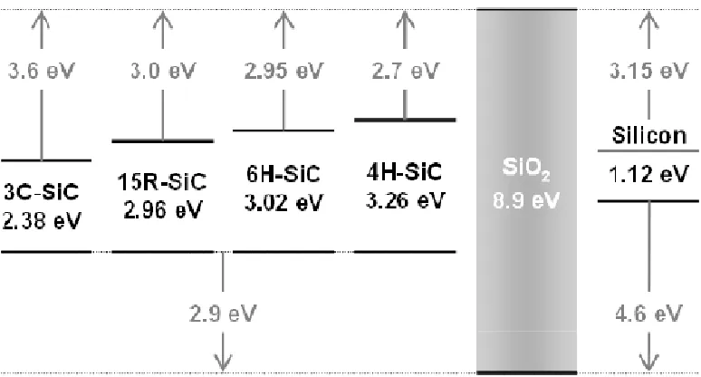
The preferred polytype for electronic applications is 4-H SiC because it has the widest
bandgap, 3.3eV. Figure 1-2 indicates bandgaps and band offsets for some common SiC
polytypes. In addition to its large bandgap, 4H SiC also has a high electron mobility which is
Figure 1-2: Bandgap and relative band offsets of several common SiC polytypes, SiO2, and Si. Information in figure is compiled from results by Afanas ev et al.5
The hexagonal crystal unit cell is shown in figure 1-3. In device processing, the most
commonly used faces are the (0001) Si-face, the (000-1) C-face, and the (11-20) a-face.
Each of these faces has a different density of carbon and silicon atoms. The Si-face consists
of 100% silicon atoms, the C-face consists of 100% carbon atoms, and the a-face consists of
50% carbon atoms and 50% silicon atoms. The differences in each of these faces lead to
Figure 1-3: Hexagonal unit cell indicating commonly used faces. Relative C and Si contents are indicated6
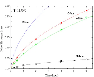
SiC forms a native oxide SiO2, in the same manner as silicon, which makes it a good
candidate for wide band-gap electronics applications because the silicon tools and technology
can be transferred for its processing. The oxidation on the Si-face of SiC is up to 10 times
thus this is not an unusual phenomenon. Oxide thicknesses obtained by dry oxidation at
1150oC on the three faces and on silicon (100) are indicated as a function of time in figure
1-4. This high temperature is required for oxides to form in a feasible time6. Such distinctive
kinetics can be related to the complex oxidation process which requires the ejection of
carbon. A net oxidation reaction9 can be written as:
2 SiC + 3 O2→ 2 SiO2 + 2 CO (1.1)
Another benefit of having a native thermal oxide is that the SiC/ SiO2 interface is
expected to be of a higher quality than that of a deposited dielectric. However, the complex
oxidation process can lead to a variety of defects at and near the interface. Because of this
complicated interface, surface conditioning, oxidation conditions, and post oxidation anneals
to control the interface have become critical in the realization of SiC technology.
1.2 Physics of Silicon Carbide Devices
SiC has much potential for high power devices which can ultimately out-perform
silicon devices. Silicon devices operating voltages are limited by the breakdown field of the
material (~3x10⁵ V/cm) and by the resulting maximum blocking voltage of PN junctions. An
overview of these areas follows.
1.2.1 Critical Field and Blocking Voltage
The kinetic energy of carriers is proportional to the electric field to which they are
subjected. In solids, they are thermalized by phonon interactions yielding a finite carrier
velocity at low fields. When this field exceeds a critical bulk value ξc, then the rate at which
a carrier gains energy is higher than the rate at which it can exchange this energy with the
lattice. In such a case, carriers in a semiconductor can reach energies which are on the order
of the band-gap energy and induce avalanche breakdown due to the multiplication of
determining the critical field where the higher the phonon energy, the higher the field at
which carriers can be thermalized. The phonon energy can be estimated using the Debeye
temperature Td. Based on this and according to the values reported in Table 1-1, the critical
field is expected to be higher in SiC than in Si. Indeed, ξc is measured to be 2.2x10⁶ V/cm in
SiC which is an order of magnitude higher than that of silicon. It is important to note that
since SiC and silicon are indirect band-gap semiconductors, the phonons are also involved in
the inter-band transitions associated with impact ionization. Both transport and breakdown
mechanisms will be discussed further in subsequent sections.
The blocking voltage of PN junctions operating in reverse bias is limited by the
current of minority carriers which can lead to an avalanche process in the space-charged
region10,3.This breakdown mechanism is similar to the one described for the bulk material. In
the case of a junction where n doping << p doping or vice versa (known as a one-sided
junction), the reverse bias leads to the depletion of carriers almost exclusively in the lower
doped region. If the highly doped region is grounded and a large positive bias Vd>>Eg/q is
applied to a lowly n-doped region, the width of the depletion layer in the step junction can be
approximated by
where εsis the dielectric constant of the semiconductor, q is the elementary charge, and Nd is
the density of positively charged donor atoms. The value of the electric field reaches a
maximum of ξmax at the junction.
(1.3)
If it is assumed that avalanche breakdown occurs when ξmax reaches ξc, then it can be derived
from equation (1.3) that the maximum blocking voltage supported by a PN junction is given
by the following.
(1.4)
Based on this, the maximum achievable blocking voltage for a given dopant concentration is
predicted to be 30 times more in a SiC PN junction than in a silicon diode.
1.3 Technology Status and Challenges
SiC-based devices have the potential to outperform silicon in high power and/or high
temperature applications, but their properties are still far from reaching the theoretical
and the interface. The feasibility of high-power MOSFETs has been demonstrated and now
reliability issues are attracting research interests. The most promising step being investigated
currently is the role and impact of NO annealing which was implemented as a part of the
device processing in 2000. This section will review properties of available substrates, the
thermal gate oxide, and the SiC/ SiO2 interface and will demonstrate that although progress
has been realized, there is still room for much improvement.
1.3.1 SiC Wafer Quality
Silicon carbide wafers have been commercially available since the 1990s. In the past
15 years, notable progress has been achieved in both the wafer size and quality. The wafer
diameter has increased from 1 inch to four inches, drastically reducing the material cost.
There are two growing steps involved in the synthesis of electronic grade single
crystalline silicon carbide. First, a SiC boule is formed using physical vapor transport (PVT)
of silicon and carbon from a heated polycrystalline seed source onto a seed crystal11. Wafers
are then created by slicing the SiC boule. Due to the high hardness of the material, polishing
is done using chemical-mechanical polishing (CMP)12. It is important to note that residual
stress can cause the wafer to bow, which causes problems for other processing steps such as
lithography13. For electronic applications, a high quality epitaxialtaxial layer (usually tens of
microns) is then grown on top of the substrate by high temperature chemical vapor deposition
wall reactors has enabled good uniformity of the epitaxial layer over large wafers and
acceptable growth rates on the order of 50µm/hour.
In order to minimize the number of stacking faults, crystals are commonly grown
along the <0001> c-axis15. This practice leads to another huge issue, that of micropipes.
Micropipe is the industry name for hollow-core dislocations which extend throughout the
substrate and act as “killer” defects limiting the yield of operating devices. Fortunately there
have been improvements in growth techniques which have led to their reduction from over
1000/cm2 in the early 1990s to approximately zero in commercially available wafers today.
Polytype inclusions have also been limited by off-axis growth (typically 8o for 4H SiC)
which yields surface steps where homoepitaxy can occur. Unfortunately, this also leads to
surface roughness and step bunching during high temperature implant annealing, both of
which negatively effect channel mobility and oxide reliability. These effects can be
minimized by using a carbon cap during activation anneals or subsequently polishing the
surface. Recent advances in CVD SiC growth have enabled the development of high quality
on axis crystals which could one day suppress the need for surface steps16.
There are other structural defects which still strongly affect device properties. Plane
dislocations can reduce the achievable blocking voltages and there are indications that
stacking faults limit the long-term reliability of SiC diode, and these stacking faults can also
play a significant role in limiting carrier lifetime which is very closely related to bulk
mobility17,18. It is worthwhile to note that the mobility is an order of magnitude lower in
p-type as opposed to n-p-type SiC; therefore currently n-channel MOSFETs are the preferred
device. However, in order to continue fruitful development of SiC technology, progress
toward fabrication of CMOS (complementary n- and p-channel MOSFETs) should be made.
1.3.2 Gate Oxide
There is very little evidence which suggests that the properties of the bulk thermal
oxide grown on SiC are different from the bulk thermal oxide grown on silicon. Raynaud19
suggested that SiC oxidation yields a stoichiometric SiO2 whose density, refractive index,
dielectric constant, and breakdown strength are very similar to those of Si thermal oxides.
Even though the SiO2 is similar in Si and SiC, the growth kinetics are quite different.
The thermal budge required to form a gate oxide of specific given thickness is ten times
higher in SiC than in Si. Because of this, it is possible to deposit CVD oxides, but a
thermally grown SiO2 layer is still necessary to ensure the quality of the SiC/ SiO2 interface.
During oxide-based device operation, charge buildup in SiO2 can occur as a result of
carrier injection. This leads to threshold voltage instability, mobility degradation, and
understand and recognize in which conditions charge buildup can occur and how it affects
the properties of the device.
When a MOSFET is in the OFF state, an electric field is present in the gate oxide and
this field can limit the achievable blocking voltages. This is directly related to the
breakdown field of SiO2 (~10MV/cm) as well as to gate leakage currents which can occur via
tunneling or emission of carrier from the gate contact. Additionally, even if the oxide field is
negligible above the base region, tunneling of the majority carrier can occur and this can
cause a trap in the dielectric within a few angstroms of the interface.
In the ON state, a bias voltage is applied to the gate which forms an inversion layer in
the base region. When high fields are present, this can lead to minority carrier injection from
the semiconductor into the oxide via Fowler-Nordheim tunneling. The distance xt that a
carrier has to tunnel in order to leak through the gate dielectric can be approximated by
φbo/ξox,where φbo is the appropriate band-offset (Volts) between the semiconductor and SiO2.
The tunneling probability is dependent exponentially on xt. Figure 1-2 illustrates that the
band-offsets of 4H-SiC relative to SiO2 are smaller than those of Si5. For a given oxide field,
this yields a leakage current in SiO2 on 4H-SiC which is always larger than SiO2 on Si. This
raises significant concerns, particularly for n-channel devices as the offset between the
conduction bands of 4H-SiC and SiO2 is only ~2.7 eV, thus promoting electron tunneling
Injection of carriers in both the ON and OFF state of device operation leads to charge
trapping in the oxide, Coulomb scatting, and interface degradation. The density of electron
and hole traps is therefore a critical parameter in determining device reliability and stability.
Understanding the SiC/ SiO2 interface is therefore critical in improving predictability and
reliability of these devices.
1.4 The SiC/SiO2 Interface
In contrast to the properties of bulk SiO2, those properties of the interface between the
oxide and the semiconductor depend strongly on the substrate and its orientation. The
quality of the interface is a critical parameter for devices and it is believed to be directly
reflected in the channel mobility of MOSFETs.
1.4.1 Scattering Mechanisms
Hall Mobility can be expressed as
(1.5)
where τ is the mean scattering time responsible for the finite speed ϋ=µξ of the carrier in a
(1.6)
The contributing processes being considered here are respectively carrier-phonon
interactions, Coulomb scattering by charged centers, carrier trapping or recombination, and
surface-roughness induced scattering. Combining equation (1.5) and (1.6) leads to the result
that the true mobility can also be written as
(1.7)
It is generally possible to determine the dominate scattering mechanism by examining the
dependence of mobility on temperature and the electric field3.
At the interface between an oxide and a semiconductor, defects and surface-inducted
states can ultimately lead to localized energy levels within the band-gap. For n-channel
devices, an electron inversion layer is formed when the amplitude of the gate bias is large
enough for the Fermi level to be close to the semiconductor conduction band edge at the
interface. In that region, most levels lying within the band-gap are filled with electrons
which reduce the density of free carriers and yields negatively charged centers. This
factors cause the mobility in the channel be expected to be lower than in bulk (e.g. the drift
region). In the case of as-grown SiO2 on 6H- and 4H-SiC, µch is indeed a fraction of µdr;
about 25 and 1% respectively20.
1.4.2 Interface Defects
Historically, the poor electrical quality of the as-grown SiO2/SiC interface has two
origins: the wide SiC band-gap and the presence of carbon. The large band-gap of SiC
makes it more susceptible to a wider range of defects than silicon. At SiO2/Si interfaces, the
presence of several electrically active defects including silicon (Si-) dangling bonds on the
substrate side21,22 and oxygen vacancies in the transition region of the oxide (Si-Si suboxide
bonds)23 have been reported. The Si- dangling bonds can be passivated by hydrogen24,25.
Additionally, a large density of levels located approximately 2.8eV below the SiO2
conduction band edge has been observed26,27, but due to their location within the Si
conduction band, these levels do not affect the channel mobility of the SiO2/Si interface. In
SiC, electron spin resonance (ESR) measurements have not yet been able to identify Si-
dangling bonds at the interface28. In addition, studies suggest that hydrogen passivation
alone is ineffective29,30,31,32, however at this point, this cannot completely be ruled out. On
the contrary, suboxide bonds can contribute to the density of levels with are electrically
active. The bonding-antibonding splitting is strongly dependent on the length of the Si-Si
silicon crystal, can contribute to levels within the silicon band-gap. These levels are
effectively passivated with hydrogen. Silicon carbide is different in that even the short bonds
lead to active interface states due to the relative position of the band edges as shown in
Figure 1-5. Theory also suggests that these short bonds cannot be readily passivated by
hydrogen29.
Figure 1-5: Schematic of the density of traps at the oxide/semiconductor interface. The relative positions of the conduction band (Ec) and valence band (Ev) edges are indicated. 4H-SiC is sensitive to a larger amount of states than 6H-SiC and silicon. This illustration is modified from a publication by Schorner et al33
Comparably, the fact that the n-channel mobility in 4H-SiC devices (≤10 cm2V-1s-1) is
lower than in 6H-SiC devices (100 cm2V-1s-1) can be attributed to levels located above the
measurements which indicate a much larger reduction (~90%) of the free electron density at
SiO2/4H-SiC interfaces as compared to SiO2/6H-SiC interfaces (~10%)20. These results also
imply that the density of states is largest close to the 4H-SiC conduction band, giving rise to
the qualitative picture for the distribution of levels illustrated in Figure 1-5.
Capacitance-voltage (CV) and conductance measurements, which have the ability to resolve the energy
distribution of the traps, indicate that the density of interface states (Dit) is in fact rising in the
upper part of the SiC band-gap and is an order of magnitude higher close to the conduction
band edge of 4H-SiC (~1013 cm-2eV-1)as compared to 6H-SiC (~1012 cm-2eV-1) for as grown
oxides (see figure 1-6). It is also important to note that the 4H-SiC n-channel mobility is
found to increase with temperature (from 200 to 475K), therefore it can be inferred that the
main mechanism limiting charge transport is Coulomb scattering of the remaining free
carriers induced by the negatively charged centers. Conversely, the 6H-SiC n-channel
mobility decreases as temperature rises (from 200 to 500K), indicating a phonon limited
transport which is less affected by interface traps. This high density of states located
between the 4H- and 6H-SiC conduction bands has not been attributed to a particular defect.
Even though it is not clear where these states should be attributed, it is clear that they
correspond to the levels which were previously observed at Si interfaces located 2.8 eV
below the SiO2 conduction band edge which is 0.1 eV below the 4H-SiC conduction band
edge and therefore within the band-gap of that polytype. These defects are generally
and wide energy distribution34,35,36,37. If these defects are related to SiO2, it would provide an
explanation for their presence in both Si and SiC. Even though 4H-SiC is generally the
preferred polytype of SiC over 6H-SiC for electronic applications because of its greater bulk
mobility, the high density of states corresponding to slow border traps only fall within its
band-gap which leads to a lower inversion mobility and higher channel resistance for its
as-grown oxide interfaces.
Another reason for the high defect density associated with the as-grown SiO2/SiC
interface is the complex oxidation process (described in equation 1-1) which necessitates the
release of carbon. Previous studies have suggested that although the oxide should
theoretically have no carbon, it is not ideally removed from the interface during oxidation.
Several techniques have found carbon in the oxide within 1 nm of the interface including
Rutherford backscattering (RBS)39,40,41,42, X-ray photo-electron scectroscopy
(XPS)43,44,45,46,47, transmission electron microscopy (TEM) with electron energy loss
spectroscopy (EELS)48,49,50, and spectroscopic ellipsometry51. As a result, it is expected that
some of these carbon related defects contribute to Dit. ESR has led to the detection of
unsaturated, three-fold coordinated carbon, which could be referred to as carbon dangling
bonds28, and XPS suggests the presence of both C-C and Si-O-C bonds.
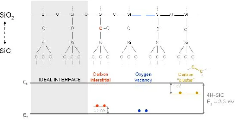
Several theoretical works have predicted defects and their respective energy levels
within the 4H-SiC band-gap. Some of these configurations are illustrated in Figure 1-7, and
more complete defects can be found in publications by Deák52,53,54 and Pantelides55,56,29. It is
found that carbon is energetically stable in a variety of configurations at the interface. For
example, a single carbon can be inserted into a Si-O-Si configuration in two ways, by
forming a Si-O-C-Si with carbon weakly linked to a silicon atom on a neighboring ring or it
can form a Si-C-Si with an oxygen protrusion. These defects are stable in the negatively
a silicon site on the substrate to occur, yielding a carbon cluster with a maximum of six
atoms. This is not unreasonable because DFT calculations have demonstrated that large
aggregates are not stable at the interface and simulations of the oxidation process have
suggested that their size is limited by carbon removal during oxidation57.
Figure 1-7: Defects which can occur at the SiC/SiO2 interface and their respective energy levels in the 4H-SiC band-gap. From Pantelides et al28
1.4.3 Interface Passivation
It is well understood that both oxidation and post-oxidation conditions can affect the
Dit distribution within the 4H-SiC band-gap. Studies conducted with argon anneals at growth
reduction of deep states. This reduction has been attributed to removal of some excess
carbon without additional oxide growth, therefore without generation of additional carbon
defects. Additionally, wet oxidations can lead to a lower Dit toward the center of the gap
when compared with dry O2, but this still does not remove the critical slow near-interface
states which contribute to the poor 4H-SiC device properties.
The effects which have been observed with water correlate with results from
hydrogen post-oxidation anneal (POA) which were performed either before or after gate
contact deposition. As mentioned earlier, hydrogen is very effective in passivating Si-
dangling bonds at the SiO2/Si interface, leading to the reduction of the Dit from
approximately 1011 to 1010 cm-2eV-1 in the middle of the silicon band-gap. This allows
silicon to achieve a high channel mobility, nearly half the value of the bulk mobility. In SiC,
hydrogen only has a limited effect and it is confined to deep interface states which are only
reduced to 1011 cm-2eV-1 , even in the presence of a catalyst cracking H2 into very reactive
radicals as seen in figure (1-8)29,30,31,32. Hydrogen annealing does not have an effect on the
slow, near-interface states. This again highlights differences in the SiO2/Si and SiO2/Si
interfaces. Due to the fact that Si- dangling bonds and long Si-Si bonds do not dominate the
Dit at the SiC interfaces, hydrogen POA is not as effective for SiC. Following H2 exposure at
theoretical predictions29, and also suggests that H2 could bind to a minority of carbon related
defects, explaining the small but noticeably beneficial effect on the Dit.
Figure 1-8: Interface trap densities in the upper half of the 4H-SiC band-gap obtained after different post-oxidation anneals. Discontinuities near Ec-E~0.6eV are the result of CV measurements taken at 23oC and 300oC, to extract D
Figure 1-9: Improved channel mobilities extracted from MOSFETs fabricated on different faces of 4H-SiC. The Si-face mobility prior to NO annealing is shown as a reference.6
One of the biggest accomplishments in the improvement of the SiC/ SiO2 interface
has been the incorporation of high temperature NO annealing into the processing procedures.
In 1997, the S. Dimitrijev’s group at Griffitth University in Australia demonstrated that high
temperature (1100oC) NO annealing effectively reduces the Dit at the SiO2/6H-SiC
interface61. After this, in 2000 Chung et al. published results on the effects of NO at the
SiO2/4H-SiC interface indicating that not only did the anneal remove deep states, it also very
efficiently reduced the density of slow states (by a factor of ten), as shown in Figure 1-8, and
ultimately led to an increase in the channel mobility an order of magnitude to 50 cm2V-1s-1,
as shown in Figure 1-9. This discovery was the result of a joint effort between Auburn
process by both scientific and industrial communities9 because it enables the fabrication of
high quality oxide based SiC power devices. Due to the fact that this is a relatively new
technology, the understanding of the NO POA benefits is not understood and is the subject of
active research within government laboratories, research universities, and companies
worldwide.
The positive impact of NO annealing has been largely attributed to the bonding of
nitrogen at the interface. Indeed, medium energy ion scattering (MEIS)6, nuclear reaction
analysis (NRA)62, secondary ion mass spectroscopy (SIMS)63, and EELS50 have indicated
that NO POA leads to a nitrogen profile located at the SiO2/SiC interface and extending 1.5
nm into the oxide. The length is comparable to that of the transition layer observed in the
oxide after oxidation. The density of the incorporated nitrogen is between 1014 and 1015
atoms/cm2. Nitrogen has also been introduced to the system in other ways including plasma
nitridation64 and NH3 or N2O POA61,65,62,66. Plasma nitridation has led to similar
improvements in the channel mobility but incorporates nitrogen throughout the oxide which
causes problems with reliability. Similarly, ammonia (NH3) also shows benefits but
incorporates unnecessary hydrogen and nitrogen in the oxide. Nitrous oxide (N2O) is
successful in localizing nitrogen to the interface but does not work as efficiently as nitric
oxide (NO). In both cases, this is because the nitrogen incorporation is related to the
fractions of N2 and O2 yielding a re-oxidation process and therefore negating the positive
effects of the nitrogen63.
After NO exposure at high temperatures, the amount of excess carbon in the oxide
near the SiO2/SiC interface is reduced. Specifically, AFM images reveal a smoother surface
after the etching of an oxide which has been NO-annealed67, and XPS measurements suggest
a reduction of the carbon related compounds at the interface and the formation of Si-N and
C-N bonds43. There are two possible origins for the benefits of NO annealing: N binding at
defect sites and/or the removal of three fold coordinated atoms following N substitution. The
binding of N at unsaturated C- and potential Si- sites can result in the formation of strong
bonds, therefore eliminating defect levels from the gap. Substitution of three-fold carbon or
silicon by nitrogen could drastically transform a given atomic configuration and therefore
affect its corresponding energy levels as well. Theoretical studies of nitrogen affinity at
defect sites located near the SiO2/SiC interface have indicated that nitrogen could in face
substitute for both silicon and carbon atoms29. One key difference between nitrogen and
hydrogen is that nitrogen is predicted to be efficient at passivating short Si-Si suboxide bonds
and C-C pairs of correlated carbons, both of which are defects that are most likely
responsible for the high Dit and the poor mobility at as-grown interfaces. NO annealing is
very efficient in the upper part of the 4H-SiC band-gap but does not lead to clear
atom brings an extra valence electron to the system. A nitrogen which is three-fold
coordinated has a lone pair of electrons in its outer shell. When this three fold coordinated
nitrogen replaces Si or C, it removes the dangling bonds in the upper part of the 4H-SiC
band-gap but also to induce a donor level associated with the lone pair close to the valence
band of the semiconductor. Even though NO annealing does not improve band states in the
lower part of the 4H-SiC band-gap, this is apparently less critical for the mobility of
n-channel devices whose value is mostly dependent on the reduction of the density of levels
close to the 4H-SiC conduction band.
It is also important to note that different forms of POA can also reduce the Dit at
interfaces formed on the a-face and the C-face of 4H-SiC, also yielding higher channel
mobilities68 as seem in Figure 1-9. Of particular interest is the a-face, which showed
improvement to 100cm2V-1s-1 in some instances69,70 , which is extremely notable because it is
twice the mobility obtained on the Si-face after NO annealing. This is an indication that even
though the Si- face has been the preferred face for device fabrication, the introduction of NO
and other POAs have changed the outlook and other faces in the material will likely be the
focus of upcoming research. An example of this is UMOSFETs, dismissed early but depend
on the a-face channel mobility71, and present several advantages worth considering with the
a-face is that it typically does not have a miscut as the Si-a-face does, yielding a more limited
surface roughening during annealing, and therefore a reduced carrier scattering.
1.5 Process optimization
In this section, three fabrication steps of oxide-based SiC devices will be discussed. They are
mentioned and described briefly in terms of their impact on device quality and reliability.
1.5.1 Channel implantation
In MOSFET design, a double implant is required to form base and source regions.
Because of this, a high temperature activation anneal (at least 1500oC) is required. There are
several problems associated with this implantation are ion-induced defects in the channel
region and surface roughening during annealing. Due to the low diffusion coefficients of the
dopant atoms in SiC, the doping cannot be achieved by driving in the dopants. A proposed
method to avoid this problem is to implement a UMOSFET design in which source and base
regions are formed by successive CVD epitaxial-growths, but this design has other problems
such as field crowding in sharp corners of the trench oxide71. High temperature annealing in
implanted devices has also been attributed to the problem of surface roughening due to Si-
emission and step bunching (as mentioned earlier, step bunching is a result of steps at the
1.5.2 Gate Oxide Growth
Gate oxide formation conditions are critical because the conditions at which the gate
oxide is formed greatly affect the quality of the SiO2/SiC interface. It has been reported that
placing alumina in the vicinity of SiC during the oxidation process leads to growth rates
which are up to 10 times faster than without the presence of alumina. The interface formed
with this process can also have a lower Dit and higher channel mobility72,73,74. Additionally,
work at Vanderbilt University has been conducted with good results exploring high pressure
growth of oxides of SiC with reduced thermal budgets9.
1.5.3 NO Annealing
The introduction of nitrogen at the SiO2/SiC interface with POA leads to a reduced
ON resistance in the channel in oxide based devices. Figure 1.10 shows data indicating that
SiC power devices can out-perform silicon devices for operating voltages down to several
Figure 1-10: Achievable specific ON resistance as a function of the designed blocking voltage for Si and 4H-SiC devices. Continuous lines indicate the theoretical limits set by the drift the drift resistance alone. Dotted lines indicate the impact of the channel resistance on the total resistance for a poor (as-oxidized) and a better (NO-annealed) interface. The symbols correspond to values extracted from actual SiC MOSFETs fabricated
before75,71,76(shown above as triangles) and after77,78,79,80 (shown above as squares) 2001.
Note, figure adapted from Rozen9.
NO annealing also facilitates faster and sharper turn-on characteristics which is important for
established, the emphasis has now shifted to the importance of optimizing the nitridation
process to avoid excess nitrogen at the interface. The impact of nitrogen on the stability of
device properties and device reliability is a focus in current SiC research because the small
band-offsets between SiC and SiO2 are a cause for concern about gate leakage upon
operation.
1.6 MOSFET Introduction
Due to the importance of MOSFET devices as potential applications for SiC, a brief
introduction to MOSFETs follows. A diagram of an n-channel DIMOSFET (DI = double
implanted) is shown in Fig. 1-11. The source and p-well regions are formed by high dose
nitrogen and low dose aluminum implants, respectively (N > 1019cm-3, Al ~ 1016cm-3). In the
absence of a positive gate voltage (right side of figure), no current flows in the device, and
the device blocks the voltage VSD applied between the source and drain. A positive gate
voltage inverts the p-well surface at the oxide-semiconductor interface (left side of figure) to
form an n-conducting channel. A large current ISD flows between the source and drain, and
the voltage drop across the device is small, resulting only from the internal resistances of
various portions of the device. Two of the important internal resistances (RCH = channel
resistance and RD = drift layer resistance) are labeled in Fig. 1-11. The “on-resistance” RON
represents the total resistance of the MOSFET to current flow and is the sum of the various
internal resistances, including RCH and RD. The on-resistance determines the internal power
Figure 1-11: Vertical DIMOSFET. Left: n-inversion channel formed by the application of a positive gate voltage VG. Right: conducting inversion channel does not form when VG is removed. Inset: Interfacial defects arising from Si-Si bonds, C-C bonds, Si dangling bonds and missing O atoms.
A convenient parameter for evaluating the performance of vertical MOSFETs is the
“specific on-resistance” or “resistance-area product” of the drift region38.
3 2 ~ C S N B SP E V R
VB is the voltage blocked by the MOSFET, µN is the bulk electron mobility in a direction
perpendicular to the oxide-semiconductor interface, εS is the permittivity of SiC and EC is the
critical field. This parameter represents the “ideal” on-resistance, neglecting any other
Gate Source (VSD)
Drain
N+
N- Drift Region
resistances in the device. The great promise of SiC can be seen in the expression for RSP,
where EC is approximately seven times larger for SiC than for Si. Lower on-resistance by a
factor of more than 300 should be possible with SiC. Significant improvements in
performance can be realized compared to Si MOSFETs for devices that operate near this
theoretical performance limit82. 4H-SiC MOSFETs have been fabricated with blocking
voltages above 10kV83. These devices have thick drift layers (~ 150µm), and the resistance
of the drift region RD dominates the on-resistance. The channel resistance is small in
comparison and does not contribute significantly to RON. However, SiC MOSFETs have
their greatest commercial potential for applications at voltages ≤ 3kV, and for these voltages,
the channel resistance can be the most important component of the on-resistance.
The low field channel resistance RCH is given by
CH N CH WQ L R
where L and W are the length and width of the channel, respectively, QN is the inversion
layer charge available for current conduction and μCH is the mobility of the electrons in the
inversion channel. The quality of the SiO2/SiC interface determines μCH and QN, which in
turn determine RCH. Clearly QN and μCH should be as high as possible so that RCH<< RD. A
large interface defect density limits QN by trapping84,85and μCH by coulomb scattering. The
CHAPTER 2: RESEARCH METHODOLOGY
In this chapter, research methodologies used to conduct atomic analysis of the
4H-SiC/SiO2 interface will be discussed. These methods include Z-contrast imaging, electron
energy loss spectroscopy, and convergent beam electron diffraction.
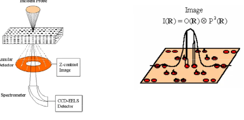
2.1 Z-Contrast Imaging with a Scanning Transmission Electron Microscope (STEM)
Z-contrast images are images in which the intensity in the image is directly related to
the square of the atomic number of the species being imaged. These images are unique
because they contain both structural and chemical information. In addition, the images can
be directly interpreted in a manner which is much more straightforward than the conventional
high resolution transmission electron microscopy (HRTEM). These images are also known
as high-angle annular dark field images86,87,88,89 and are formed by scanning a highly focused
electron beam (convergence angle α~ 15-35 mrad) across the surface of the sample material
and collecting those electrons which are scattered to high angles (40-100 mrad at 200kV in
the JEOL 2010F 90) on a high-angle annular dark field detector. This setup can be seen in
Figure 2-1: a)schematic of the STEM b) the experimental image can be interpreted as a simple convolution of the experimental probe and the object function
By using high angles and integrating over a large angular range, coherence effects between
near neighbors can be minimized91,92. Based on this, in the approximation of large collection
angles, each atom can now be considered an independent scattering source with a scattering
cross-section of approximately Z2, where Z is the atomic number. The object function is
effectively formed by this cross-section in a manner such that the object function is
maximized at the atom sites. This means that for specimens thin enough such that the
dynamical diffraction effects can be neglected, the detected intensity is a convolution of this
object function with the probe intensity profile (figure 1)93,94. Due to the small width of the
microscope, which has been shown to be as small as 0.6Ả for a spherical aberration corrected
(Cs corrected) STEM at 300kV95. In crystalline materials in a zone-axis orientation, the
atomic spacing is greater than the probe size therefore the columns are illuminated
sequentially as the probe is scanned over the specimen and an atomic resolution
compositional map is subsequently generated.
The same is also true for thicker specimens. It has been noted that for specimens in
zone-axis orientation, the STEM probe forms narrow spikes around each atomic column as it
propagates through the material 96. This effect is known to be caused by the coherent nature
and large angular spread of the STEM probe, leading to the tightly bound s-type Bloch states
adding constructively and the less localized states interfering destructively 93 94. This effect
is increased for scattering processes localized at atomic cores, such as high-angle thermal
diffuse scattering (TDS), causing a great reduction in beam broadening. With only one
dominant Bloch state, dynamical diffraction effects are largely removed and are manifested
only as a columnar channeling effect, thus maintaining the thin specimen description
described above.
Finally, Z-contrast imaging is highly desirable because the phase problem which is
associated with the interpretation of HRTEM images is eliminated. In thin specimens, the
dominant contribution to the intensity of the image is always its composition, and the effect
the surface of the specimen. For any defocus away from the optimum Scherzer condition,
the probe broadens, lowering resolution such that the individual atomic columns cannot be
resolved. The optimum focus is realized when the maximum intensity is present in a narrow
probe profile without the presence of significant probe, thus assuring the localization of the
image information. This is also the optimum probe for microanalysis 97,98,99,100,101. The other
important advantage of Z-contrast imaging is that simultaneous with the image chemical
analysis through electron, energy-loss spectroscopy is also possible.
2.2 Atomic Resolution Electron Energy Loss Spectroscopy (EELS)
Figure 2-1 illustrates the experimental setup for data collection within the TEM. It is
clear based on this figure that the annular detector which is used for Z-contrast imaging does
not interfere with the low-angle scattering used for EELS. This means that the Z-contrast
image can be used to position the electron probe over a specific structural feature for the
acquisition of a spectrum 97,98,99,100,101. This simultaneous analysis allows for direct chemical
Figure 2-2: A typical EELS spectra
The basic physical principal behind EELS relates to the interaction of fast electrons with the
sample to cause either collective excitations of electrons in the conduction band, or discrete
transitions between atomic energy levels, e.g. 1s→2p transitions 102. The ability to observe
discrete atomic transitions allows compositional analysis to be performed by EELS due to the
fact that the transitions occur at characteristic energy losses for a given element.
Additionally, the transitions to unoccupied states above the Fermi level allows the degree of
hybridization between atomic orbitals to be determined, that is, information on local
electronic structure (bonding) changes can be established. Figure 2-2 shows a typical EELS
In order to accurately analyze the chemical content of the samples, a new method
called "QuantiFit,” developed by our research group headed by Dr. Gerd Duscher, is used. In
order to extract bonding information of the atoms, we analyze the shape of the element
specific ionization edges known as the electron near edge structure (ELNES)103,104. Based on
these two techniques we develop a clearer understanding of the atoms present and their
bonding configuration.
A very important aspect of this study is the necessity to be able to correlate the EELS
spectrum with a particular location on the sample. This requires that the spectra have the
same spatial resolution as the Z-contrast image. In order to achieve this resolution, the range
over which an electron can cause an excitation event must be less that the inter-atomic
spacing105. Hydrogenic models106 indicate that for the majority of the edges which are
accessible through conventional energy-loss spectrometers (ΔE < 2keV) the object functions
are localized within 0.1nm of the atom cores107,108. In other words, the object function is
localized at the atom cores in the same way as the Z-contrast image and an experimental
probe of atomic dimensions. An important aspect of this experimental approach is that the
probe channeling effect discussed for Z-contrast imaging also preserves the spatial resolution
of the spectrum, thereby allowing atomic resolution analysis of the electronic structure to be
2.2.1 Qualitative Compositional Analysis
A core loss in EELS occurs when the incident electron beam excites a core level
(K,L,M,N,O) electron in a material and therefore loses energy (see figure 2-2 to identify core
loss region of EELS spectrum). This excitation process (also known as inner-shell ionization
process) contains elemental information, therefore it plays an important role for
compositional analysis.
In the EELS spectrum, this process is reflected as an ionization edge of triangular or
saw-toothed shape. Its start energy is defined by the minimum energy loss (ionization
threshold or critical ionization energy Ec) which is required to overcome the nuclear electron
binding energy. Based on this, the critical ionization energy is specific for each element and
can thus be used for elemental identification in EELS. In general, the intensity in the
core-loss region on the EELS spectrum is maximum at Ec because this is the point with the highest
scattering probability (cross section). For energy losses greater than Ec, the atomic electron
can still be ionized, but the probability is less than at Ec, therefore the intensity in the EELS
spectrum drops sharply.
In addition to elemental identification, bonding information such as coordination
number and charge state can also be revealed by shifts in the ionization edge. For example,
in silicon, for the L2,3 edge, Lopatin109 reported that there is roughly a 6eV shift between
Figure 2-3 EELS linescan across the Si/ SiO2 interface indicating a 6 eV shift in the L3,2 edge onset109
Inner shell ionization usually occurs at high energies (>50eV). Additionally, Ec
increases for K shell ionization as the atomic number increases, therefore L and M edges are
more practical for elements with a large atomic number. One negative effect of using L and
M edges is that their ionization is often edge overlapping, especially at low energies. There
are several examples of this which will not be discussed because they are not part of this
thesis. The primary core edges studied in this work are the Si L3-2 edge, the C K edge, and
2.2.2 Quantitative Compositional Analysis
Integration of ionization edges in EELS can yield quantitative information. After
subtraction of the background, the ratio of elements present can be determined following this
relation NA
, Δ , Δ ·
, Δ , Δ
where IA and IB are the integrated intensities of element “A” and “B” and σA and σB cross
sections of element “A” and “B”.
It is important to note that in reality, the ionization edges in an EELS spectrum are
much more complex than a simple Gaussian peak. Ionization edges are always superimposed
on the Plasmon peak. The Plasmon peak is due to the low loss interaction between the
incident electron beam and out-shell weakly bonded electron, and it occurs at energies
<50eV. These interactions are particularly important for our study because some of our
EELS spectra show interaction between the Si L2-3 edge and the Plasmon peak. The second
complication with ionization edges is that it is very unusual to get a sample which is thin
enough for the ideal single scattering. Instead, electrons from the incident beam can undergo
multiple scattering events. This plural scattering takes place not only in the Plasmon region,
but also 15-20eV above the ionization edge. Finally, the fine structure information is
Conventional quantification methods have been developed to remove the background
and fit the edges. There are two main methods used, each with sources of error. The first
method utilizes a power law background fit of the form AxE-r where A and r are fixed
parameters and E is the energy loss. This method is based on the theory of the Plasmon
resonance decay of a free electron gas. This method ignores the variation of r observed in
real experiments and thus does not accurately model the background of a real EELS
spectrum. The second method is described by Verbeeck and Aert110 and features edges
which only account for the free electron state. More recent ab initio calculations111,112 prove
the existence of solid state effects within the first 50 eV after the edge onset, complicating
edge fitting and causing errors within Verveeck and Aert’s method.
Due to the problems described in the preceding paragraph, Dr. Duscher’s group
developed a new quantification method, QuantiFit. QuantiFit follows the same physical
principles as Verbeecks and Aerts method but also adds two modifications. (1) A linearly
combined power law and polynomial fitting for the background (instead of the power law
alone), and the addition of a polynomial fit. The polynomial fits act like a variation of the
parameter r and higher orders (3rd and 4th order) to produce a change in the curvature
allowing for more degrees of freedom and ultimately a better fit. The interference of solid