Article
1
Optimised performance of non-dispersive infrared
2
gas sensors using multilayer thin film bandpass
3
filters
4
Pinggui Wang 1,2, Xiuhua Fu 1*, Des Gibson 2**, Lewis Fleming 2, Cheng Li 2, Manu Muhiyudin 2,
5
Shigeng Song 2, David Hutson 2, David Moodie 3, Calum MacGregor 3 and Mathew Steer 4
6
1 Changchun University of Science and Technology, Changchun 130012, China;
7
2 Scottish Universities Physics Alliance (SUPA), The institute for Thin Films, Sensors & Imaging, University
8
of the West of Scotland, Paisley, PA1 2BE, U ;
9
3 Gas Sensing Solutions Ltd, 60-62 Grayshill Road Westfield North Courtyard Cumbernauld G68 9HQ, UK;
10
4 Scottish Universities Physics Alliance (SUPA), University of Glasgow, ; Glasgow, G12 8QQ, UK;
11
* Correspondence: 13604435770@126.com; Tel: +86 13604435770
12
** Correspondence: Des.Gibson@uws.ac.uk; Tel.: +44-(0)771-198-5621
13
14
Abstract: In this work performance improvements are described of a low power consumption
15
non-dispersive infrared (NDIR) methane (CH4) gas sensor using customised optical thin film
16
bandpass filters (BPF). BPF’s shape the spectral characteristic of the combined mid infrared III-V
17
based light emitting diode (LED)/ photodiode (PD) light source/ detector optopair, enhancing NDIR
18
CH4 sensor performance. The BPF, deposited using a novel microwave plasma assisted pulsed DC
19
sputter deposition process, is deposited at room temperature directly onto the temperature sensitive
20
PD heterostructure. BPF’s comprise germanium (Ge) and niobium pentoxide (Nb2O5) alternating
21
high and low refractive index layers respectively. Two different optical filter designs are progressed;
22
with BPF bandwidths (BWs) of 160 nm and 300 nm. Comparison of modelled and measured NDIR
23
sensor performance is described, highlighting maximized signal to noise ratio (SNR) and minimized
24
cross talk performance benefits. BPF spectral stability for various environmental temperature and
25
humidity conditions is demonstrated.
26
Keywords: NDIR; methane; sensor; infrared; thin film; III-V, heterostructure; bandpass;
27
microwave; sputter; MBE
28
29
1. Introduction
30
There are increasing requirements to monitor and control the concentration of methane (CH4) in
31
such fields as environment, landfill sites, fracking facilities, security, industry and agriculture [1-4].
32
CH4 is a flammable and explosive gas and is the main component of natural gas. CH4 becomes
33
explosive when concentration in air are in the range of typically 5% (lower explosion limit (LEL)) [5,
34
6]. Invisible and odourless CH4 gas leaks can pose a threat to human life.
35
Coal mine gas accidents are caused by the rapid increase of methane concentration in a short
36
period of time, not only posing a serious threat to the safety of miners, but can also results in
37
substantial economic losses [5]. In addition to the health and safety of oil & gas industry personnel,
38
CH4 gas sensing finds relevance in the detection of atmospheric concentrations of CH4 where
39
increased emissions will contribute to the greenhouse effect. As a result phenomena such as rising
40
temperatures and sea levels and frequent occurrence of extreme weather events will pose a serious
41
threat to food security, ecosystems, and our living environment.
42
At present, the methods for monitoring methane concentration are based on various detection
43
methods, including electrochemical [7], gas chromatography [8], thermal conductivity [9], catalytic
44
combustion [10, 11], photoionization [12] and NDIR [13–15]. Among these methods, NDIR gas
45
sensor is the preferred sensing method due to simple operation and maintenance, long service life,
46
fast response time, high measurement accuracy and fail to safe operation [13–15].
47
NDIR gas sensors comprise an infrared light source, optical BPF and a detector. The light source
48
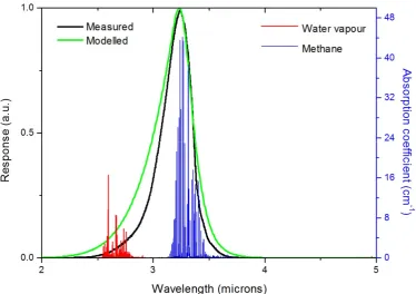
emits infrared light at a wavelength tuned to the infrared (IR) absorption of gas in the optical path
49
between the source and detector. This results in a reduced IR intensity incident on the photodetector.
50
Typically optical BPF`s are incorporated to improve the NDIR gas selectivity by narrowing the total
51
BW of the spectral response of the source-detector system and thereby preventing cross sensitivity
52
with other gases and water .
53
By measuring the incident light intensity I0 and the transmitted light intensity I of the IR light, the
54
concentration of methane gas concentration can be calculated according to the Beer-Lambert law
55
[27]. A state-of-the-art NDIR CH4 gas sensor has been utilised for this work [16], utilizing a
56
molecular beam epitaxy grown pentanary alloy light emitting diode (LED) light source and
57
photodiode (PD) detector, shown in figure 1(a). For this work the stoichiometry of the
58
semiconductor source-detector pair is tuned for maximum spectral response at 3.3 μm, coinciding
59
with a principle absorption band of the CH4 molecule, due to the asymmetric stretch vibrational
60
mode [20].
61
This work describes direct deposition of BPF`s directly onto the LED/ PD optopair, thereby
62
optimizing spectral response shape. A room temperature deposition method suited to direct
63
deposition onto the temperature sensitive LED/ PD optopair is described and associated optical BPF
64
environmental (temperature and humidity) performance.
65
2. Relevant Background Work & Non Dispersive Infrared Sensor Configuration
66
Work was previously carried out by Fleming et al [17] in the deposition of 300 nm BW bandpass
67
filters onto commercially available LEDs and photodiodes. This previous work related to carbon
68
dioxide (CO2) detection for breath monitoring (capnography) during surgical anaesthesia [18, 19]. It
69
was found that application of the coating onto the photodiode only (as opposed to coating the LED
70
only or both LED and PD) with the bandpass filter design was the optimum method to isolate the
71
CO2 absorption band and reduce cross-talk effect from the commonly used surgical anaesthetic gas
72
nitrous oxide (N2O) [28]. The light emitted from the mid infrared LED is reflected from a gold coated
73
injection moulded plastic dome geometry optic onto the PD. A CH4 mid infrared absorption band at
74
3.3 μm coincides with a CH4 anti-symmetric stretch vibrational mode. Another band exists in the
75
long-wave infrared (LWIR) and peaks at 7.6 μm. According to HITRAN database [20], the
76
absorption intensity of methane gas is the largest at wavelength 3.3 μm and as such this band was
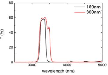
77
chosen for CH4 detection in this work.
78
79
(a) (b)
For this reason, a bandpass BW of 300 nm is chosen for this work, and builds upon the previous
81
work by comparing the effect of a narrower BW (160 nm) bandpass filter. A BW of 300 nm was
82
originally chosen as this matches the BW of the 3.3 μm CH4 absorption band. The optical coating
83
designs were built into a comprehensive NDIR gas sensor Mathcad model and their effects on the
84
sensor signal accuracy and reduced cross sensitivity determined, specifically adjacent water
85
absorption band at 2.8 μm [20]. A gas sensor model predicting the measured sensor signal as a
86
function of gas concentration was established using Mathcad [21]. The model includes the
87
temperature dependent LED spectral emission and PD spectral detectivity using a generalised form
88
of the Planck equation [22, 23]. Gas species’ spectral absorption characteristics are imported from the
89
HITRAN database and are used to model the effect on the sensor signal as a function of gas
90
concentration, comprising various gas mixtures in the sensor light source/ detector optical path
91
length using the Beer-Lambert law. The model includes influence of Johnson-Nyquist noise, dark
92
noise and also quantisation noise is a result of the modelled data collection electronics. Theoretical
93
description of the model is provided in Section 3 of this paper.
94
Figure 2 shows the modelled and measured spectral response of the CH4 sensor indicating good
95
agreement between the theoretical and experimental result. Also plotted in figure 2 are the
96
absorption coefficients for CH4 and water vapour (H2O). It can be seen that the CH4 absorption band
97
peak coincides with the peak of the sensor spectral response for both the modelled and experimental
98
curves. The H2O absorption peak lies in close proximity to the CH4 peak and as a result, lies within
99
the spectral response of the CH4 sensor, suggesting that the sensor will suffer from cross-talk (i.e.
100
unwanted signal contribution) from H2O if it is present in any significant concentration. When the
101
sensor chamber contains water vapour, this can cause significant inaccuracies in detected CH4
102
concentration. Therefore, it is advantageous to use optical filtering to reduce the influence of other
103
gases and improve the selectivity of the detection system. In addition, different bandpass filter
104
designs can provide a method to influence the NDIR gas sensor detection accuracy and sensitivity.
105
The primary purpose of this paper is to design the technical parameters of the bandpass filter
106
according to the demand of the NDIR gas sensor and demonstrate room temperature direct
107
deposition onto the LED/ PD optopair, removing the need for inclusion of a separate discrete
108
bandpass filter.
109
111
Figure 2. Modelled total sensor spectral response, semi-empirical sensor response and CH4 and H2O absorption
112
coefficients.
113
114
3. Theoretical Background
115
3.1. Determination of bandpass filter parameters
116
The total gas sensor spectral response is determined by
117
𝐺 𝜆 = 𝑆 𝜆 ∗ 𝐷 𝜆 , (1)
where S is the spectral response of the source and D is the spectral response of the detector. The gas
118
sensor will be sensitive to any gas with an absorption band that lies within the spectral region of G.
119
When a gas species is present with an absorption band that lies within G, the spectral response
120
follows:
121
𝐺 𝜆 = 𝑆 𝜆 ∗ 𝑇 𝜆 ∗ 𝐷 𝜆 , (2)
where Tg is the optical transmittance of the gas which follows the well-known Beer-Lambert law:
122
𝑇 𝜆 = 𝑒𝑥𝑝 −𝛼 𝜆 ∗ 𝑐 ∗ 𝑙 , (3)
Where; α is the absorption coefficient of the gas, c is the concentration and l is the pathlength that
123
the light travels through. Analogously, the total spectral response of the source-detector system can
124
be modified by using an optical interference filter with optical transmittance Tf . The new total
125
spectral response for a filtered sensor Gf becomes:
126
To maintain maximised NDIR sensor sensitivity to the target gas, the Tf must have maximum
127
optical transmittance over the gas absorbing spectral region and necessary blocking of unwanted
128
signal contributions from other gases and water vapour. Tf must be as close to zero as possible over
129
the absorbing regions of such gases. In this work an optical bandpass filter spectral characteristic
130
mathematical function was modelled using Mathcad 15 and incorporated into a comprehensive gas
131
sensor model. The LED source emission was approximated using the generalised Planck equation
132
and the photodiode detectivity was modelled using the characteristic equations for a photodiode
133
response [24]. From this the modelled NDIR gas sensor signal response incorporating bandpass filter
134
was modelled. The multilayer bandpass filter structure was modelled using thin film optical design
135
software TFCalc, where the multilayer optical filter structure was designed such that the modelled
136
optical transmittance matched that of the bandpass filter spectral characteristic function modelled in
137
the Mathcad NDIR gas sensor program. From the TFCalc [29] model, the exact layer thicknesses and
138
number of layers for each coating design were used as the basis for experimental deposition of the
139
multilayer bandpass filters. The influence of 2.67 μm infrared absorption peak of water vapour,
140
angle offset and signal-to-noise ratio were taken into account during the filter design stage. Two
141
different bandpass filters (table 1) were designed based on sensor signal modelling results (table 2)
142
for maintaining good sensor accuracy up to the CH4 LEL and good blocking of H2O absorbing
143
wavelengths that are a considerable cause of cross-talk for this sensor design. The results show that
144
the accuracy of 300 nm is lower than the accuracy of 160 nm, but is still highly adequate.
145
146
Table 1. Comparison of technical parameters between 160 nm and 300 nm band pass filter
147
Bandpass Filter Parameter
160 nm BW filter
300 nm BW filter Central
wavelength (μm)
3.3 3.325
FWHM (nm) 160 300
T (peak) 73% 85%
Blocking (μm) 2-5 2-5
148
Table 2. Comparison of accuracy between 160 nm and 300 nm band pass filter
149
CH4 concentration
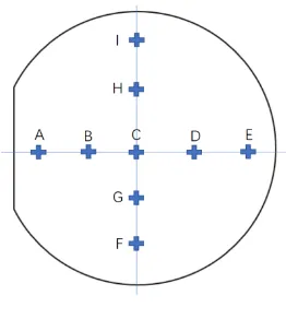
range (ppm)
160 nm BW filter (%)
300 nm BW filter (%)
10 – 100 6.2 7.7
100 – 1000 0.6 0.8
1000 – 50000 0.01 0.02
150
3.2. Design of the 300 nm and 160 nm BW optical bandpass filters
151
A three cavity Fabry-Perot BP was modelled in TFCalc, as a starting design for both the 300 nm
152
and 160 nm BW bandpass filters. Next, a computational optimisation technique was used to alter the
153
multilayer design in order to achieve two different bandpass filter designs, one with a 300 nm and
154
one with a 160 nm BW passband, both with good out of band blocking to reduce signal contributions
155
from other gases.
156
For the 300 nm BW bandpass filter, the structure consists of 34 layers and the total thickness is 10.6
157
um, the peak transmittance reached 60%, while the average transmittance in the out of band regions,
158
2-3 μm and 3.6-5 μm are 0.09% and 0.32%, respectively, and the SNR of filter is 2.4%. For the
159
peak transmittance reaches 58%, the average blocking area of 2-3.1 μm and 3.5-5 μm is 0.12% and
161
0.31%, with a SNR of 4.5%.
162
163
Figure 3. Measured spectral characteristics for optimised 300 nm BW bandpass and 160 nm BW bandpass filter
164
designs.
165
166
4. BPF Deposition Method & Materials
167
4.1. Multilayer thin film optical interference filter preparation method
168
In this work, thin film optical coatings were prepared using a novel microwave plasma-assisted
169
pulsed reactive DC magnetron technique. The system used is shown in figure 4. The apparatus is
170
equipped with a complete microwave generator system comprising a 6 kW microwave magnetron
171
head, tuner and microwave delivery tubes. Reactive plasma ion density is greatly enhanced via use
172
of this external microwave source, which results in a greater reactive gas reactivity and generates a
173
greater number of monoatomic ions which results in greater coating uniformity and reduced optical
174
absorption in the applied coatings. Use of pulsed DC power greatly reduces the problem of arcing
175
caused by target poisoning and positive charge build up on the sputtering target surface and aids
176
achieving a higher film deposition rate. In this work, thin films Ge and Nb2O5 were obtained by
177
sputtering from Ge and niobium (Nb) bulk sputtering targets, each with 99.999% (5N) purity.
178
The deposition rate and thickness of the film are monitored in real-time by quartz crystal thin film
179
thickness monitors [30], utilsing three crystals per magnetron. Argon is used as sputter process gas
180
and oxygen as a reactive gas. At the same time, the pressure and flow rate of gas are accurately
181
controlled by an optical gas controller (OGC) and MKS mass flow controllers controlled by a
182
multi-gas controller. The chamber body is heated by hot water to liberate any residual H2O
183
molecules trapped on the chamber walls and into the molecular flow regime, thereby increasing
184
their probability of becoming trapped by Meisner cooling coils in the vacuum chamber (Telemark
185
polycold model 3600).
186
Removal of water vapour is essential for the growth of high quality mid-infrared optical coatings
187
where film density and water content play a significant role in determining the films optical
188
absorption and spectral stability. Typical system ultimate vacuum is 5 x 10⁻⁷ mbar, minimizing
189
adverse influence of water vapour on the optical BPF performance of the film is reduced. By
190
adjusting deposition process parameters, required quality and low absorption Ge and Nb2O5 single
191
layer films were deposited for optical characterization, essential for the design and manufacture of
192
multilayer thin film optical BPF`s. Specific process parameters used are shown in Table 3. This
193
system was used to deposit two different BPF`s - specifically 300 nm BW and 160 nm BW, directly
194
deposited onto Gas Sensing Solutions (GSS) Ltd NDIR gas sensor photodiodes for comparison of
195
influence on gas sensor performance. Also included in each coating run was a 100 mm (4”) undoped
196
(a) (b)
Figure 4. (a) Schematic of the microwave plasma-assisted sputter reactor used to deposit thin optical films
198
described in this work and (b) image of the actual chamber. Right and left hand side magnetrons were used,
199
populated with Ge and one Nb target material.
200
201
Table 3. Deposition process parameters used to grow thin films of Ge and Nb2O5. 10 kWAdvanced Energy
202
magnetron drive (MDX) power supplies were used in voltage regulation and current regulation mode for Ge
203
and Nb2O 5 respectively to drive the sputtering process.
204
Material Ge Nb2O5
MDX power
(kW) 2.5 2.84
MDX current
(A) 6.1 7.75
MDX voltage
(V) 410 367
Argon flow
(sccm-1) 190 190
O2 flow (sccm-1) 0 75
O2 partial
pressure (Torr) 0 6*10-4
Microwave
plasma power 0 3
Deposition rate
(nms-1) 0.1 0.18
205
4.2. Optical characterization
206
Optical transmittance in the mid-IR for single and multilayer coatings were obtained using a Nicolet
207
iS-50 Fourier Transform Infrared (FTIR) spectrometer. The optical constants which are essential for
208
multilayer thin film optical filter design (refractive index and absorption coefficient) were derived
209
from the optical transmittance spectra using a combination of the O’Leary, Johnson and Lim (OJL)
210
model [25] for amorphous materials and the Drude model. The TFCalc thin film design software was
211
then used to design a band pass filter meeting the required specification, and calculate the deviation
212
between the design and the experimental results. Gas sensor photodiode spectral photocurrent
213
response for uncoated and coated diodes was measured using a Bruker VERTEX 80/80v FTIR,
214
216
4.3. Gas sensor testing
217
Calibrated gas sensors were placed in a testing chamber at room temperature and exposed to a gas
218
mixture of N2 (which is IR inactive so does not elicit a response in the sensor) and CH4. The CH4
219
concentration was controlled by varying the continuous flow rate ratio provided by a CH4 mass flow
220
controller (MFC) and an N2 MFC. A range of 0 ppm – 50000 ppm CH4 was used and was chosen as
221
50000 ppm is the LEL for CH4.
222
223
5. Results & Discussion
224
5.1. Thin film optical constant derivation
225
Single layers were deposited onto 500 μm thick gallium arsenide (GaAs) substrate. Optical
226
transmittance spectra for single layer 1 μm Ge and 1.5 μm Nb2O5 as measured using FTIR is shown
227
in figure 5 and overlain with the uncoated GaAs substrate spectrum for comparison. The calculated
228
optical constants are shown in figure 6. It can be seen that the absorption coefficient of the thin film
229
materials are small, and the refractive index contrast between the Ge and Nb2O5 thin films is large,
230
suggesting that these materials are acceptable material candidates for use in the fabrication of mid
231
infrared multilayer optical BPF`s.
232
233
Figure 5. Optical transmittance spectra of GaAs substrate, Ge single layer and Nb2O5 single layer.
234
(a) (b)
Figure 6. Optical constants for (a) thin film Ge and (b) thin film Nb2O5 as calculated by using a combination of
235
the OJL and Drude models.
236
5.2. Multilayer thin film optical interference bandpass filter deposition
238
Two different bandpass filter Ge/Nb2O5 multilayer designs were deposited onto GSS methane sensor
239
photodiodes using precision laser cut masking to mask the rest of the bridgeboard LED structure.
240
The spectral transmittance characteristic curve of each bandpass filter was obtained using the
241
Nicolet iS-50 FTIR on the witness samples present during the coating runs. Figure 7 shows excellent
242
agreement between the theoretical design and measured results of the two optical BPF`s. It can be
243
seen that the actual transmittance of the 160 and 300nm BPF`s are 57% and 58% respectively, in
244
excellent agreement with the design values. This is because deposited thickness was greater than the
245
model resulting in a slightly higher optical absorption. However, this slight mismatch between
246
theory and design is negligible as the bandpass CWL and BW remains the same – the two critical
247
parameters for maintaining gas sensor sensitivity to CH4 and for out of band blocking of the H2O
248
infrared absorption band centred at 2.67 um. Bandpass filter design parameters for 160 nm BW and
249
300 nm BW are shown in table 1.
250
251
(a) (b)
Figure 7. Comparison between theory and experimet for (a) 160 nm BW bandpass filter and (b) 300 nm BW
252
bandpass filter designs.
253
254
5.3. Uncoated and coated gas sensor photodiode photocurrent spectral response
255
The aforementioned coatings were applied to the GSS CH4 gas sensor LED/ PD bridgeboards
256
tuned for emission and detection at the CH4 absorbion wavelength at 3.3 μm. The bridgeboard was
257
masked apart from the photodiodes, enabling the optical coating to be applied to the photodiode.
258
Using a Bruker VERTEX 80/80v FTIR, the spectral response for the uncoated and coated diode
259
heterostructure was recorded. Figure 8 shows the BPF influence on the photodiode photocurrent
260
(a) (b)
Figure 8. Overlay of coated and uncoated CH4 photodiode photocurrent response coated with (a) 160 nm BW
262
bandpass filter and (b) 300 nm BW bandpass filter. The spectral characteristics for the measured witness
263
samples are also shown. It can be seen that in both cases, the photodiode photocurrent response shapes conform
264
to the shape of the optical filter spectral characteristic.
265
It can be seen that the coated photodiode photocurrent response is shaped by the optical filter
266
spectral transmittance characteristic. Application of the optical BPF provides significant reduction in
267
photodiode BW photocurrent response, and hence the total sensor spectral response is reduced,
268
lowering the response at wavelengths outwith the CH4 absorption band with the aim of minimising
269
sensor response to gases other than CH4 and also improving the accuracy of the sensor for the CH4
270
target gas. Here it is demonstrated that different optical filter designs can be readily applied to the
271
sensor photodiode, allowing for a greater flexibility in sensor design and the ability to customise and
272
optimise NDIR gas sensor design to specific customer applications.
273
274
5.4. Gas sensor testing results
275
The signal as a function of time for a 160 nm BW BP and a 300 nm BW BP coated sensor is shown in
276
figure 9. The sensors were calibrated for temperature compensation and then exposed to a nitrogen
277
(N2)/CH4 gas mixture where the CH4 concentration was cycled between 0%, 2.5% and 5% CH4
278
concentration over a duration of 4 hours. From figure 9, it can be seen that both the 160 nm and 300
279
nm BW BP coated sensors show a similar response to this variation in CH4 concentration. As
280
expected, the SNR performance of the 300 nm BW BP coated sensor is superior to the 160 nm BW BP
281
sensor as a result of a greater intensity of IR light transmitted through the BPF.
282
284
Figure 9. Calibrated sensor signal response for 160 nm BW BP and 300 nm BW BP coated sensors when cycled
285
from 0 ppm, 25000 and 50000 ppm methane (LEL) over the course of 4 hours. Inset plot shows an exploded
286
view of the signal at 5% methane, highlighting the different noise characteristic between the 300 nm BW BP
287
coated sensor and the 160 nm BW BP coated sensor.
288
289
For this reason, we suggest it is suggested the 300 nm BW BP filter is a better choice than the 160
290
nm BW BP filter as it has an improved SNR performance. Table 4 shows the calculated
291
root-mean-square (RMS) noise for 5%, 2.5% and 0% CH4 for both the 160 nm BW BP coated and 300
292
nm BW BP coated sensors. Generally RMS noise increases with increasing gas concentration as more
293
light is absorbed and less light is incident on the sensor photodiode. The calculated values for 2.5%
294
and 0% methane for the 160 nm BW BP sensor do not reflect this, however the authors suspect this to
295
be due to the small sample size collected for 2.5% methane.
296
297
Table 4. Calculated RMS noise for 160 nm and 300 nm BW BP coated sensor signals.
298
Methane percentage (%)
160 nm BW BP coated sensor (a.u.)
300 nm BW BP coated sensor
(a.u.)
5 3.6×10⁻⁴ 1.9×10⁻⁴
2.5 2×10⁻⁴ 1.8×10⁻⁴
0 2.4×10⁻⁴ 1.1×10⁻⁴
299
5.5. Wafer uniformity test
300
Work has previously been carried out by Cheng et al [26] in testing coating thickness uniformity in
301
bridgeboards were mounted onto specially designed tooling with precision masking in order to
303
apply the coating to the photodiode surface area only, however, this method may not be optimal for
304
scalable mass production of coated photodiodes. A more optimal method would be to sputter
305
deposit the coating onto an enitre photodiode wafer directly after it has been grown by MBE prior to
306
dicing and mounting onto sensor bridgeboards. For this reason, both the 160 nm and the 300 nm BW
307
bandpass filter optical coating designs were each successfully deposited onto 100 mm diameter ( 4”)
308
<100> undoped silicon (Si) wafers with 500 μm thickness grown by the czochralski method and
309
tested for coating uniformity to demonstrate that the bandpass filter spectral characteristic is
310
uniform over an entire 4” wafer and thus suitable for coating an entire newly grown photodiode
311
wafer.
312
313
314
Figure 10. Schematic of 4” Si wafer as mounted onto the microwave plasma-assisted sputter coater drum.
315
Post-coating, the wafer was diced into 20 x 20 mm sections and the optical transmittances was measured for
316
samples A – I to test for coating thickness uniformity. This was done for both 300 nm and 160 nm BW bandpass
317
filters.
318
The Si wafer was mounted onto the deposition system’s rotating drum such that the wafer flat was
319
parallel with the circumference of the drum as depicted in figure 10. Post coating, the wafer was then
320
diced into 20 x 20 mm squares and each section’s position was labelled and measured using FTIR to
321
compare the spectral variation in their optical transmittances. The results for the 160 nm and 300 nm
322
BW bandpass filters are plotted in figure 11.
323
324
(a) (b)
Figure 11. (a) Optical transmittance spectral characteristics for different Si wafer location samples A-I for the
325
160 nm BW bandpass filter. (b) Optical transmittance spectral characteristics for different Si wafer location
326
samples A-I for the 300 nm BW bandpass filter.
327
From these spectra, the coating uniformity was calcaulted for both the 300 nm badwidth bandpass
329
filter and the 160 nm BW bandpass filter and the results are shown in table 4.
330
331
Table 4. Thickness uniformity across a 4” Si wafer for two different optical filter designs.
332
Filter BW (nm)
Thickness uniformity from center of
the 4” Si wafer (%)
160 ±0.355 300 ±0.530
333
These small deviations show that satisfactory coating thickness uniformity can be achieved across an
334
entire wafer maintaining the desired optical transmittance spectral characteristic by maintaing good
335
optical transmittance over the CH4 absorption band and adequate blocking at H2O absorption
336
wavelengths, suggesting that coating an entire photodiode wafer prior to dicing and mounting onto
337
electronics bridgeboards may be a production efficient way of incorporating optical filters into NDIR
338
gas sensor architectures.
339
340
5.6. Accelerated lifetime testing
341
A common accelerated lifetime test to probe the optical and structural integrity of thin film coatings
342
is to use subject the samples to the pressure cooker test, where coated witness samples are subjected
343
to a prolonged exposure to high temperature and high pressure using a pressure cooker. Perhaps
344
more relevant to optics in extreme conditions such as those for high velocity windows for military
345
aircraft or coatings for machinery tooling, the pressure cooker test is a good indicator of coating
346
durability in harsh environments. The center piece of the coated Si wafer for both the 160 nm BW
347
bandpass and the 300 nm BW bandpass were placed into the cenetr of a pressure cooker with
348
maxiumum pressure of 15 psi. The samples were subjected to cooking times of 5, 10, 20 and 40
349
minutes and had their optical transmittances measured by FTIR in between each step.
350
351
(a) (b)
Figure 12. Optical transmittance of (a) 160 nm and (b) 300 nm BW bandpass witness sample after being
352
subjected to 15 psi inside a pressure cooker for varying durations.
353
From figure 12 it can be seen that the optical filter spectral characteristic remained largely the same
355
for all times, where a small reduction in peak transmittance was observed for the 160 nm BW
356
bandpass filter. For the 300 nm BW bandpass filter the only minimal change in peak optical
357
transmittance occurred for 5, 10 and 20 minutes, however, the drop in transmittance was more
358
pronouned for 40 minutes. For Differences between the 160 nm BW and the 300 nm BW bandpass
359
samples are most likely to be attributable to the top layer being different, where for 160 nm, the top
360
layer was Ge and for 300 nm it was Nb2O5.
361
The diode surface that the coatings were applied to is an unpolished underside of GaAs (so-called
362
flip-chip method was used to bond the sensor diodes to the electronic bridgeboard, where the
363
upwards facing surface of the element is the backside of the substrate that the MBE grown material
364
was deposited on) therefore factors such as high substrate surface roughness may also be a factor in
365
determining the coatings mechanical integrity for the actual gas application sensing, however,
366
coatings applied to the gas sensor photodiode element will not be subjested to such a harsh
367
environment, so it can be safely assumed that disruption of the coatings optical properties is unlikely
368
to occur.
369
370
5.7. Humidity & temperature testing
371
Gas sensors in different temperature and humidity environment, the performance parameters will
372
be changed, so it is necessary to do the humidity and temperature tests of the optical filter. The
373
closed central pieces of the coated Si wafer for both the 160 nm BW bandpass and the 300 nm BW
374
bandpass were placed into the WKL Temperature and Climatic Test System. The humidity test was
375
carried out at 50 ℃ and 95% humidity for 24 hours and the temperature test is -40 ℃ to 70 ℃ where
376
the temperature was increased by 10 ℃ every two hours.
377
378
(a) (b)
Figure 13. Optical transmittance of (a) 160 nm and (b) 300 nm BW bandpass witness sample after humidity test.
379
(a) (b)
Figure 14. Optical transmittance of (a) 160 nm and (b) 300 nm BW bandpass witness sample after temperature
381
test.
382
383
6. Conclusion
384
In this work, the spectral response of a methane sensor comprising a heterostructure LED and PD
385
optopair was modelled and compared with the experimentally measured spectral response giving
386
good agreement. The accuracy of such an NDIR gas sensor was modelled from the modelled spectral
387
response. Next, single layers of Nb2O5 and Ge were deposited onto optical substrates and optically
388
characterized to obtain their refractive indices and extinction coefficients which were subsequently
389
used in the design of two multilayer optical interference BP filters; one with a passband of 300 nm
390
BW and one with 160 nm BW. These designs were then sputter deposited onto MBE grown
391
heterostructure diodes with peak detectivity tuned to 3300 nm (in order to coincide with the CH4
392
absorption band to be used in the interest of CH4 gas detection) using microwave plasma-assisted
393
pulsed DC magnetron sputtering. The thin film multilayer filters were also deposited onto full 4” Si
394
wafers in the same coating run. The coated and uncoated PD PC responses were measured using a
395
FTIR and it was demonstrated that the PD PC spectral response conforms to the spectral shape of the
396
applied optical filter for both 300 nm and 160 nm BW BP filters. These coated PDs were then built
397
into gas sensor electronics with full injection molded plastic optics and tested under various CH4 gas
398
concentrations for comparison. Gas concentration was cycled from 0%, 2.5% and 5% CH4
399
concentration, to test the sensor’s capability in measuring concentrations of CH4 below the LEL. As
400
expected it was observed that the 160 nm BW BP coated sensor displayed more noise as compared
401
with the 300 nm BW BP sensor, most likely due to the reduced intensity of IR incident of the PD and
402
therefore a poorer SNR. The 160 nm BW BP coated sensor, having a narrower BW as compared with
403
the 300 nm BW BP coated sensor, will be less susceptible to cross-talk inducing gases, so it is difficult
404
to assess which optical coating design is superior given this cross-talk/noise level tradeoff. Noise
405
levels could be electronically filtered out at the expense of lowering the measurement frequency of
406
the sensor, therefore the different BW optical filter coatings designs may be suited better to different
407
applications with different measurement frequencies and accuracy requirements.
408
In addition to testing of improvement of gas sensor performance using multilayered optical
409
coatings, coating uniformity and structural integrity tests under various environmental conditions
410
were carried out. As mentioned, the multilayer filters were deposited onto full 4” Si wafers. The
411
wafers were then diced and the optical transmittance of each section was measured, showing
412
excellent thickness uniformities of +/-0.355% and +/-0.530% for 160 nm and 300 nm BW BP coatings
413
respectively. This demonstrates that full production wafers can be successfully coated and
414
subsequently diced without disruption to the optical coating, which suggests that full PD
415
the multilayer thin film optical filter were then subjected to accelerated lifetime testing using a
417
pressure cooker to expose the coating to high heat and high pressure for different lengths of time.
418
The optical transmittance was measured after 5, 10, 20 and 40 minutes to observe the effect on the
419
optical properties of the coating. It was found that no significant shift occurred up to 40 minutes,
420
however a slight change in peak transmittance was observed, hypothesized to be due to absorption
421
of H2O into the film matrix. The witness samples were also subjected to less severe but longer
422
duration temperature and humidity testing in an environmental chamber. The samples were
423
subjected to a humidity test where they were exposed to 50oC and 95% RH for 24 hours, after which,
424
the optical transmittance was measured. The temperature test comprised of exposing the coating to a
425
temperature range of -40oC to 70oC where the temperature was held for 2 hours at each temperature
426
and ramped up by 10oC every 2 hours – after this test the optical transmittance was also measured.
427
For both the temperature and humidity tests, no significant change in the optical transmittance of
428
the samples was observed suggesting that the deposited films are highly dense and are unlikely to
429
undergo delamination in conditions in which the CH4 gas sensor would be present.
430
431
References
432
1. Mitchell, J.F.B. The “Greenhouse” effect and climate change. Rev. Geophys. 1989, 27, 115,
433
doi:10.1029/RG027i001p00115.
434
2. Zhang, T.; Nix, M. B.; Yoo, B. Y.; Deshusses, M. A.; Myung, N. V. Electrochemically
435
functionalized single-walled carbon nanotube gas sensor. Electroanalysis 2006, 18, 1153–
436
1158, doi:10.1002/elan.200603527.
437
3. Christensen, T.H.; Cossu, R.; Stegmann, R. Chapter 3, Landfilling of waste: Biogas, 1st
438
edition, Taylor & Francis, Oxford, England, 1996, 0419194002
439
4. Tchobanoglous, G; et al. Chapter 1, Integrated Solid Waste Management - Engineering
440
Principles and Management Issues, 1st edition, King, P.H.; Eliassen, R. McGraw-Hill
441
International editions, USA, 1993, 0071128654
442
5. Braker, W.; Mossman, A.L. Matheson Gas Data Book, 7th edition, Yaws, C.L, McGraw-Hill
443
Professional, USA, 2001, 0071358544
444
6. Britton, L.G. Using material data in static hazard assessment, Process Safety Progress, 1992,
445
1, 56-70, https://doi.org/10.1002/prsb.720110209
446
7. Dreisbach, F.; Staudt, R.; Keller, J. U. High pressure adsorption data of methane, nitrogen,
447
carbon dioxide and their binary and ternary mixtures on activated carbon. Adsorption 1999,
448
5, 215–227, doi:10.1023/A:1008914703884.
449
8. Tadesse, K.; Smith, A.; Brydon, W. G.; Eastwood, M. Gas chormatographic technique for
450
combined measurement of hydrogen and methane using thermal conductivity detector. J.
451
Chromatogr. A 1979, 171, 416–418, doi:10.1016/S0021-9673(01)95325-7
452
9. Lee, J. H.; Trimm, D. L. Catalytic combustion of methane. Fuel Process. Technol. 1995, 42,
453
339–359, doi:10.1016/0378-3820(94)00091-7.
454
10. RAE Systems by Honeywell Staff The PID Handbook—Theory and Applications of
455
Direct-Reading Photoionization Detectors (PIDs); 3rd ed.; 2013; ISBN 0976816210.
456
11. Zhu, Z.; Xu, Y.; Jiang, B. A one ppm NDIR methane gas sensor with single frequency filter
457
denoising algorithm. Sensors (Switzerland) 2012, 12, 12729–12740, doi:10.3390/s120912729.
458
12. Tan, Q.; Tang, L.; Yang, M.; Xue, C.; Zhang, W.; Liu, J.; Xiong, J. Three-gas detection system
with IR optical sensor based on NDIR technology. Opt. Lasers Eng. 2015, 74, 103–108,
460
doi:10.1016/j.optlaseng. 2015.05.007.
461
13. Hodgkinson, J.; Tatam, R. P. Optical gas sensing: A review. Meas. Sci. Technol. 2013, 24,
462
12004–59, doi:10.1088/0957-0233/24/1/012004.
463
14. Dinh, T. V.; Choi, I. Y.; Son, Y. S.; Kim, J. C. A review on non-dispersive infrared gas sensors:
464
Improvement of sensor detection limit and interference correction. Sensors Actuators, B
465
Chem. 2016, 231, 529–538, doi:10.1016/j.snb.2016.03.040.
466
15. Gas Sensing Solutions Available online: https://www.gassensing.co.uk/ (accessed on Jul 2,
467
2018).
468
16. A Novel Solid State Non-Dispersive Infrared CO2 Gas Sensor Compatible with Wireless and
469
Portable Deployment”, D Gibson, C MacGregor, Sensors. 2013; 13(6):7079-7103 (May 2013).
470
17. Fleming, L.; Gibson, D.; Song, S.; Li, C.; Reid, S. Reducing N2O induced cross-talk in a
471
NDIR CO2 gas sensor for breath analysis using multilayer thin film optical interference
472
coatings. Surf. Coatings Technol. 2018, 336, 9–16, doi:10.1016/j.surfcoat.2017.09.033.
473
18. Gas Sensing Solutions. Available online: https://www.gassensing.co.uk / (accessed on
474
30/07/18)
475
19. Mipex Tech. Available online: https://mipex-tech.com (accessed on 30/07/18)
476
20. Rothman, L. S et al, J. The HITRAN 2008 molecular spectroscopic database. J. Quant.
477
Spectrosc. Radiat. Transf. 2009, 110, 533–572, doi:10.1016/j.jqsrt.2009.02.013.
478
21. PTC Mathcad. Available online: https://www.ptc.com/en/products/mathcad (accessed on
479
30/07/18)
480
22. Smestad, G.P. Generalized model of a solar converter, Optoelectronics of Solar Cells, 1st
481
edition, SPIE press, 2002
482
23. Smestad, G.; Ries, H. Luminescence and current-voltage characteristics of solar cells and
483
optoelectronic devices. Sol. Energy Mater. Sol. Cells 1992, 25, 51–71,
484
doi:10.1016/0927-0248(92)90016-I.
485
24. Rieke, G. Detection of Light; Cambridge University Press: Cambridge, 2002; ISBN
486
9780511606496.
487
25. O’Leary, S.K.; Johnson, S.R.; Lim, P.K. The relationship between the distribution of
488
electronic states and the optical absorption spectrum of an amorphous semiconductor: An
489
empirical analysis, J. Appl. Phys. 82, 3334 (1997); doi: 10.1063/1.365643
490
26. Li, C.; Song, S.; Gibson, D.; Child, D.; Chu, H. on; Waddell, E. Modeling and validation of
491
uniform large-area optical coating deposition on a rotating drum using microwave plasma
492
reactive sputtering. Appl. Opt. 2017, 56, C65, doi:10.1364/AO.56.000C65.
493
27. Pierre Bouguer, Essai dʹoptique sur la gradation de la lumière (Paris, France: Claude
494
Jombert, 1729) pp. 16–22.
495
28. Fleming, L, 2018. Reducing N2O induced cross-talk in a NDIR CO2 gas sensor using
496
multilayer thin film optical interference filters. Ph.D thesis. Paisley: The University of the
497
West of Scotland
498
29. Software Spectra Inc. 2018. http://www.sspectra.com/. [ONLINE] Available at:
499
30. Inficon. 2018. IC 5 thin film deposition controller manual. [ONLINE] Available at:
501
https://products.inficon.com/getattachment.axd/?attaName=f23367c6-34f1-446a-814a-832704