ABSTRACT
KUPFERSCHMIDT, JAMES R. Reliability of Gap Capacitors. (Under the direction of Jon-Paul Maria and Angus Kingon.)
The requirements for communication devices continue to become more aggressive each year leading to rapid developments in varying technologies to meet the demands. Tunable filters, utilizing ferroelectric varactors, are merely one solution to the ever-demanding need for microwave communication systems. Barium Strontium Titanate (BST) can be employed as the dielectric material necessary to make tunable devices. The broad range of BST’s remarkable properties allow for easy integration into many devices, such as MEMS, oscillators, phase shifters, and tunable filters. BST deposition is done via RF magnetron sputtering for our purposes. Previous work completed here at NCSU has led to a sophisticated process to fabricate tunable filters chips that work over the 6-18 GHz range. Using polycrystalline alumina substrates with varactors composed of a pair of 4 μm gap capacitors in series as well as the utilization of the BST dielectric creates excellent tunable chips. There is however issues related to the reliability of the gap capacitors that make-up the varactors.
Weibull statistics, via the Bernard median rank equation for determining cumulative probability, are utilized to analyze the breakdown data. Various mechanisms lead to breakdown occurring among these capacitors and further investigation into silver electromigration was undertaken to explore the possibility of migration as a significant factor towards failure.
The details involved in fabricating tunable filters is detailed and shown to be relatively similar to the construction of samples with many gap capacitors; however, the process involved in fabricating tunable filters is of course much more cumbersome and also only produces a few gap capacitors. BST thin-film deposition is completed initially, followed by photolithography processes to define the outline of the gap capacitors. Silver metallization is accomplished using DC magnetron sputtering, and patterning is completed by lift-off in an acetone solution, due to the lack of harmful effects to the BST thin-film. Samples with roughly 250 gap capacitors on them were also fabricated on alumina substrates, with gaps ranging between 2 to 5 microns and widths between 100 to 750 microns. Large numbers of the gap capacitors were placed under ramping DC bias to observe if failure occurred using a suitable probe station. Proper analysis was undertaken using Weibull statistics, and several critical variables were examined, including roughness, patterning processes, adhesion of silver metal to the substrate, as well as varying types of ground metals. SEM was utilized in examining the capacitor failure, including carrying out experiments looking into silver electromigration.
Reliability of Gap Capacitors
by
James Kupferschmidt
A thesis submitted to the Graduate Faculty of North Carolina State University
in partial fulfillment of the requirements for the Degree of
Master of Science
Materials Science and Engineering
Raleigh, North Carolina 2008
APPROVED BY:
_______________________________
Jon-Paul Maria
Associate Professor
Materials Science and Engineering Chair of Advisory Committee
______________________________ Angus Kingon
Professor Engineering
BIOGRAPHY
James Richard Kupferschmidt was born in St. Paul, Minnesota during a terrible thunderstorm on July 15, 1980 to Marlys and Gary Kupferschmidt. He attended Stillwater Area High School from 1996 – 1999. During his high school career, he ran track and cross country and also played trumpet in the symphony band and orchestra. Upon completion of high school, he enrolled at Iowa State University in Ames, IA to pursue a degree in Chemical Engineering. During his time at Iowa State, he completed internships and co-ops with Penford Products and 3M. Also while at ISU, he conducted research into biochemistry and copper deposition under the direction of Dr. Charles Glatz and Dr. Kurt Hebert respectively. Upon completion of his degree in Chemical Engineering, James took a job with Cardinal Float Glass in 2005 as a process engineer.
ACKNOWLEDGMENTS
There are a great many people I owe a debt of gratitude to during my time here at NCSU. First off, I need to thank both of my parents, Gary and Marlys Kupferschmidt, as well as my brother, Mark Kupferschmidt (as well as his new wife, Tina). Without their support and guidance in my life, I would not be where I am today. I also need to thank other members of my extended family, including my Grandmother, aunts and uncles, as well as all of my many cousins. I also extend a meaningful thank you to my godparents, Richard and Beverly Rausch, as well as their family, for their constant presence in my life and for which I am forever grateful. You have all made this work so much more meaningful, and thus I thank you from the bottom of my heart.
TABLE OF CONTENTS
LIST OF TABLES... vi
LIST OF FIGURES ... vii
Chapter 1: Introduction ... 1
1.1Ferroelectric Material BST ... 1
1.2BST-Based Devices Considerations ... 2
1.3History of and Motivation for looking into Capacitor Failure... 5
1.4The Theory Developed to Understand Capacitor Breakdown... 7
1.5Statistical Analysis of Breakdown Results ... 10
1.6Mechanisms and Other Concerns for Breakdown ... 13
Chapter 2: Experimental Procedure ... 16
2.1 Filter Processing... 16
2.1.1 BST Thin-Film Deposition ... 16
2.1.2 Photolithography... 18
2.1.3 Metallizations and Lift-off... 18
2.2 Capacitor Fabrication... 22
2.3 Failure Testing ... 23
2.4 Breakdown Statistics... 24
2.5 Methods for Determining Causes of Breakdown and Electromigration Experiments ... 30
Chapter 3: Mechanisms and statistics of silver gap capacitor failure on alumina substrates . 33 3.1 Abstract ... 34
3.2 Introduction... 34
3.3 Experimental Procedure... 36
3.4 Results and Discussion ... 39
3.4.1. Ag Gap Capacitor Failure on Alumina Substrates Without BST ... 39
3.4.2. BST Incorporated as a Dielectric for Ag Gap Capacitors... 42
3.5 Discussion... 46
3.6 Conclusions... 48
3.7 References... 49
LIST OF TABLES
LIST OF FIGURES
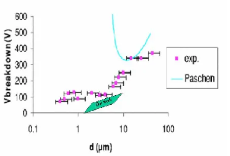
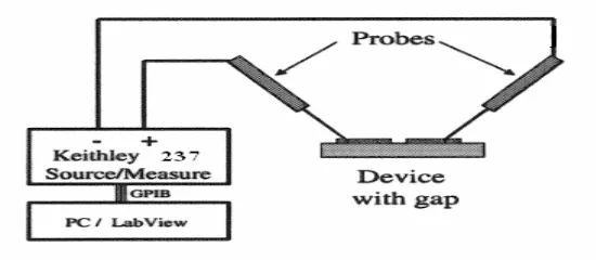
Figure 1.1: The area of our experimentation into capacitor breakdown in relationship with previous work and Paschen’s Law – adapted from E. Hourdakis, et al... 8 Figure 1.2: Presentation of breakdown data using Weibull statistical analysis and the Bernard median rank for cumulative probability. The data in this figure show breakdown of 0.35 micron thick Ag gap capacitors on alumina with an annealed BST dielectric ... 12 Figure 1.3: Capacitor failure of a 4-micron wide silver gap capacitor on an alumina substrate (0.35 μm thickness Ag)... 14 Figure 2.3.1: The probe station setup for capacitor breakdown studies ... 23 Figure 2.4.1: Cumulative probability of breakdown field for 2-micron wide gap Ag
capacitors (0.35 μm thick) on alumina with and without BST ... 24 Figure 2.4.2: Comparison of the cumulative probability of 4 micron Ag gap capacitors
patterning processes ... 26 Figure 2.4.3: Experimental data comparing the cumulative probability of breakdown for 2
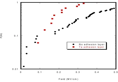
μm gap capacitors with and without a Ta adhesion layer... 27 Figure 2.4.4: 2 μm Ag gap capacitor (0.35 μm thickness) breakdown statistics on various substrates... 28 Figure 2.4.5: Breakdown statistics showing cumulative probability of 2 μm gap capacitors with varying metals (thickness of 0.35 μm) on alumina substrates... 29 Figure 2.5.1: Images depicting the occurrence of silver electromigration after applied bias. 31 Figure 2.5.2: EDS line scan showing the presence of an electro-migrated silver wire inside the gap... 32 Figure 2.5.3: An EDS point scan also confirms the existence of silver electromigration ... 32 Figure 3.4.1.1: IV curve showing electrical failure of silver gap capacitor... 39 Figure 3.4.1.2: Cumulative probability of breakdown field for Ag MIM capacitors on
Figure 3.4.2.1: Cumulative probability of breakdown field for silver gap capacitors on
alumina with BST ... 43 Figure 3.4.2.2: Cumulative probability of breakdown field for 2-micron wide gap Ag
Chapter 1: Introduction
1.1Ferroelectric Material BST
The necessity of devices working over wide ranges of frequencies for communication systems has become vital as of recent for uses in wireless phones, Bluetooth, satellites, and antennas. For these systems to be functional, it is essential to have frequency agile devices. The devices must be small, inexpensive, and efficient thus presenting considerable materials challenges. Tunable filters, imploring the use of a ferroelectric dielectric, allow for components to be tuned over broad frequencies. Ferroelectrics offer exceptional properties, including tunability with applied voltage, low losses, and the capability to manage enormous power loads. Tunability, which is of enormous importance to ferroelectric materials, is dependent on dielectric permittivity. One such ferroelectric material that has been the subject of extensive research 1-4 is Barium Strontium Titanate, BaxSr1-xTiO3, or BST.
crystal system of BST is dependent on temperature, in which tetragonal (polar) structure is found above the Curie temperature and cubic structure is obtained below the Curie temperature. Dielectric permittivity rises to a peak at the Curie temperature, and when these materials are cooled below the Tc, spontaneous polarization occurs, which strains the crystal
structure. To minimize strain, the crystal exhibits domain structure, which is the trademark of ferroelectric materials. Curie temperature and the lattice parameter both are dependent on the barium to strontium ratio 7. The permittivity is also affected by the (Ba+Sr)/Ti ratio, where the higher the percentage of titanium, the lower the permittivity 8,9. Crystallization of BST films is necessary for densification and can be done at elevated temperatures above 700ºC 10. As thickness of the BST thin-film decreases, the dielectric constant will decrease as well 3,9. Roughness of the thin-film also increases as BST’s thickness increases – this change in roughness can lead to changes in the interface properties as well as changes in the skin depth effect, leading to a change in the overall loss tangent 1.
1.2BST-Based Devices Considerations
⎥ ⎥ ⎦ ⎤ ⎢ ⎢ ⎣ ⎡ − = ) (min ) (max ) (min ) ( * 100 (%) V V V n ε ε ε
where ε is the measured dielectric permittivity at the minimum and maximum applied voltages. The overall device quality factor is given by:
C R C R Q Q Q S P conductor BST total ω ω + = +
= 1 1 1
1
where C is the capacitance, RS is frequency independent, and RP is associated with the losses
due to BST.
Dielectric loss tangent is a measure of the loss-rate of power of a mechanical mode and is determined by: C Rp ω δ 1 tan =
The BST dielectric can be deposited by a variety of methods, including physical vapor deposition (e.g. radio frequency, or RF magnetron sputtering), chemical vapor deposition (e.g. metalorganic chemical vapor deposition or MOCVD), and chemical solution deposition (e.g. sol-gel).
the use of this substrate material incredibly appealing. Cost, size, availability, loss tangent, dielectric constant, and coefficient of thermal expansion (CTE) are all factors that must be considered when selecting the substrate material. The majority of microwave devices up to this point have been on expensive substrates such as LaAlO3 21, single-crystal Al2O3
(sapphire) 21, and MgO 22. All of these substrates offer extremely low loss tangent values and other design advantages. Polished polycrystalline alumina (purity>99.6%) substrates were selected for use in this study due to the low expense ($85 for a 4.5” x 4.5” x 0.015”), high-quality microwave properties (low loss tangent of 10-4), high dielectric constant, and a similar CTE (~9 ppm at room temperature) to BST (~9.8 ppm at 300 K), which allows for annealing at high temperatures without cracking of the thin film 18. Other substrates considered for use in tunable filters in our later studies included high resistivity silicon (HRS) and sapphire.
further investigations included using tantalum as an adhesion layer with silver as the top electrode, and then eventually a Cr-Au electrode.
The functional aspect of tunable filters is made up of varactors with capacitors that are tunable by applied bias. The capacitors that were implored for use in our tunable filters were metal-insulator-metal (MIM). These capacitors exhibit vertical polarization, and the capacitance value is derived from:
) / ( 0 A t
C =ε εr
where ε0 is the permittivity, εr is the dielectric constant, A is the area of the electrodes, and t
is the thickness of the dielectric. Reliability of capacitors is a serious issue requiring consideration when design takes place. Electrical breakdown is likely to occur between electrodes separated by incredibly small gaps and is crucial to many different technologies. The design and operation of such devices requires a clear knowledge and understanding as to the sources of failure as well as the breakdown voltage.
1.3History of and Motivation for looking into Capacitor Failure
As previously explained, understanding capacitor failure is of utmost importance to a variety of technologies. Research regarding failure of capacitors goes back to the 1950’s
24-26, and very little research has been undertaken between then and relatively recently. The
semiconductors is down at the tens of nanometers level 27-29. In tunable filters for example, the spacings between capacitors is on the order of a few microns and high voltages can be applied across the gaps leading to exceptionally large electrical fields. The breakdown of gap capacitors is detrimental to the operation of the devices and leads to leakage current, so a clear understanding as to mechanisms of the breakdown and the breakdown voltage itself are critical.
One must also consider capacitor breakdown from the standpoint of our everyday lives. Circuit breakers routinely contain banks of capacitors in parallel where existing theory reveals 110 volts is not large enough to create an arc. However, existing theory has been shown and will be shown again in this thesis to be incorrect once the electrode spacings become extremely small (down in the range of a few microns), so this new information begs the question as to whether 110 V would be enough to short out the new miniaturized circuit breakers leading to a fire. Also, automobiles are going through an upgrade in their electrical system and changing their operating voltages from 14 V to 42 V 30. This increase in voltage could undoubtedly lead to more failures for the electrical systems in automobiles, hopefully none leading to any catastrophic accidents. Capacitor plague 31,32 also continues to be a
1.4The Theory Developed to Understand Capacitor Breakdown
Figure 1.1: The area of our experimentation into capacitor breakdown in relationship with previous work and Paschen’s Law – adapted from E. Hourdakis, et al.
with smaller spacings. This mechanism is not particularly relevant to our area of study since the tunable filters for our uses have gap spacings of less than 5 μm, so as we have already stated another mechanism is taking place.
So, the phenomena of electric field emission and tunneling have been studied and applied to small gap failure 37. For gaps of less than 5 μm, the electric field is obviously very large, which leads to the ability of electrons with energies less than the Fermi level to physically tunnel through the deformed surface potential barrier by field emission. The change in current is due mainly to the surface potential barrier’s field dependence. Sometimes referred to as cold emission or Fowler-Nordheim tunneling, field emission requires electrons with adequate energies to rise above the potential barrier for the ability to overcome the condensed phase. To determine field emission, the Fowler-Nordheim equation establishes the relationship between the current density and the work function as well as the electric field. Regardless of the work function or temperature, large electric fields (such as those created between small gaps or around sharp edges) aid in the tunneling of electrons out of the cathode in field emission cathodes 38. Electrode material and surface roughness affect breakdown voltage when field emission occurs as well 35. At extremely small gaps of less
contacts that are currently in use, which generally contain sharp edges. So, Paschen’s Law is still applicable for gap spacings over 10 μm; however, with much smaller gaps, field emission of electrons occurs, which is not in agreement with Paschen’s Law.
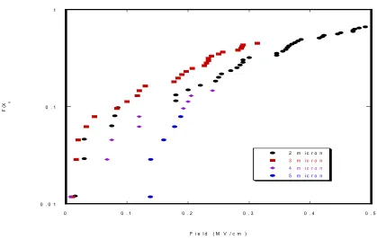
1.5 Statistical Analysis of Breakdown Results
To better understand electrical breakdown, there must be knowledge of not only the mechanisms of breakdown but also the statistics. The appropriate statistical methods are necessary to not only assess the material’s quality, but also predict the reliability of components for future devices as well as the lifetime of an electrical system. Another rationale for developing statistical models for breakdown is that it can give some general ideas as to the causes and mechanisms of failure. When failures of electrical components occur, outages happen, as well as the replacement of generally expensive electrical equipment. For our purposes, Weibull statistics can be used to explore capacitor failure. Due to flexibility, the Weibull distribution can be used for field of life data. This ability allows for the mimicking of behavior of other statistical distributions, for example the exponential or the normal.
to go about obtaining the cumulative probability, but this issue was resolved in the late ‘80s by Fothergill 39 using Monte Carlo simulations to test four equations used for cumulative probability where he found “excellent agreement between the median rank approximation and the exact calculated values.” So, the Bernard median rank equation is then applied to determine the cumulative probability of failure:
4 . 0
3 . 0 )
(
+ − =
n i x
F i
where i represents the whole number corresponding to the ranking for the failed capacitor, and n is the total number of capacitors tested. This method for determining cumulative probability is the most acceptable and is an improvement over other cumulative probability methods, including F(xi) = i/n. This information can then be plotted as such by graphing
F(xi) vs. electrical breakdown field as shown in figure 1.2, and Monte Carlo simulation is one
0 . 0 1 0 . 1 1
0 0 . 1 0 . 2 0 . 3 0 . 4 0 . 5
2 m i c r o n 3 m i c r o n 4 m i c r o n
5 m i c r o n
F (
X i)
F i e l d ( M V / c m )
Figure 1.2: Presentation of breakdown data using Weibull statistical analysis and the Bernard median rank for cumulative probability. The data in this figure show breakdown of 0.35 micron thick Ag gap capacitors on alumina with an annealed BST dielectric
1.6Mechanisms and Other Concerns for Breakdown
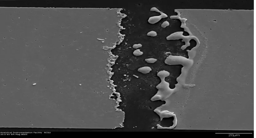
Figure 1.3: Capacitor failure of a 4-micron wide silver gap capacitor on an alumina substrate (0.35 μm thickness Ag)
coining of the word silverware. The applications and testing of various MW and RF devices usually occurs at atmospheric conditions, which can lead to concerns related to their reliability. One more consideration for the occurrence of electromigration is surface characteristics, since nucleation sites are required for dendrites to initiate and grow. The rough surface of the alumina offers the perfect location for migration to occur.
Chapter 2: Experimental Procedure
In this chapter, the experimental procedure developed to construct tunable filters using BST dielectric varactors is presented, since the procedure is very similar in nature to the processing necessary to produce samples of MIM capacitors. Experiments were undertaken to improve and understand the reliability of the capacitors making up the varactors. The techniques used to produce tunable filters were developed previously by Peter Lam and others formerly working on the AMESAT project. Experiments with the intention of understanding and providing statistical analysis for capacitor breakdown were undertaken to correlate and improve tunable filters.
2.1 Filter Processing
Construction of tunable filters is a multiple day, complex process that requires many steps. Also, the steps involved are similar, and in order, to obtaining samples containing only banks of capacitors. Below is the outline for a procedure developed to produce tunable filters necessary for this project.
2.1.1 BST Thin-Film Deposition
using 4” diameter stoichiometric BST (with a barium to strontium ratio of 70/30) target (Super Conductors Materials, Inc., Suffern, NY). The barium to strontium ratio of 70 and 30 respectively was chosen to provide optimal conditions for tunability and losses. Prior to sputtering, the substrates were cleaned in acetone and methanol and then dried for 5 minutes at 115ºC. During deposition, the platform where the substrate is located can be heated and rotated to allow for homogeneous deposition during sputtering. Vacuum inside the sputtering chamber is insured by a turbo pump and is roughed by a rotary vane pump. The chamber is first lowered to a pressure of 5x10⁻⁵ Torr, and then pure flowing argon is pumped into the chamber to produce a pressure of 1x10⁻² Torr for sputtering.
2.1.2 Photolithography
To prepare for the metallization, photolithography was necessary via a negative development process in clean room conditions. The substrates were initially cleaned using acetone and methanol solutions followed by drying on a hot-plate at 115ºC for five minutes. The resist, Shipley 1813 (Laurell Technologies Corp., North Wales, PA), was spun at 4000 rpm for 50 seconds to produce a flat surface with a thickness of 1.5 μm for further lithography on to the alumina substrates and was followed up by a soft-bake at 90ºC for 2 minutes allowing for the resist to harden. A mask containing the proper outline for tunable filters was then utilized and aligned using a MA 6 Karl Suss Contact Mask Aligner in soft contact mode and put into contact with the substrate followed by a short exposure to UV light (λ= 365 nm at I = 15 mW/cm2). A hard-bake of the substrate took place after the exposure at 115ºC for 90 seconds. Next, the entire sample was exposed to UV light via a flood exposure for 90 seconds. Lastly, a developing solution (Microposit MF-319, Laurell Technologies Corp., North Wales, PA) was used for 30 seconds to complete the lithography process, and final inspection of the sample was done using an optical microscope.
2.1.3 Metallizations and Lift-off
without the substrate inside and pre-sputtering of the silver takes place for 3 minutes at 20 mTorr of pure-flowing argon. The chamber is then reopened, and the substrate is placed inside, and the system is pumped down to 5x10⁻⁵ Torr again. Once more, argon is pumped into the chamber to obtain a pressure of 20 mTorr (this pressure allows for good adhesion and few impurities), and the deposition of Ag takes approximately ten minutes thereafter to obtain a thickness of 0.35 μm. A 1” Ag target (Kurt Lesker, Clairton, PA) is used for the deposition at a power of 100 W at a distance of 5.5 cm.
After deposition is complete, the metal for the devices needs to be patterned by a lift-off process in acetone. This lift-lift-off process was chosen due to its use of benign organic chemicals that do not damage the BST thin films. Another option for fabricating the very fine features of MW devices is by etching. However, the etchant solution will react with and damage the BST layer as well as produce toxic products. The sample must then be dried after lift-off by using nitrogen, and the features are then examined with an optical microscope. The backside of the substrate is also metallized with a seed-layer of Cr and Cu using a DC sputtering system similar to the one mentioned above to achieve a thickness of ~150 nm, which acts as a ground plane. A copper layer is then deposited on top of the silver by electroplating through the vias in a copper sulfide solution for several minutes. This procedure allows for a thicker top electrode of approximately 4-5 μm.
breakdown strengths were discovered. A dual deposition chamber was utilized for depositions where an adhesion layer was necessary. The vacuum for this chamber was once again sustained by a diffusion pump roughed by a rotary vane pump. A water-cooled rotatable substrate holder was implored to mount the samples inside the chamber. Water-cooling was necessary to ensure the photoresist on the samples did not become too warm during deposition. The chamber was initially pumped down to 1 x 10⁻⁶ Torr, and both metals were deposited through DC sputtering. During deposition, the sample would be directly in the line-of-sight of the sputtering source. Pure flowing argon (99.99%) was again used as the sputtering gas. Both targets were presputtered so as the sputtering metal would be free of impurities and clean. Once presputtering was complete, the substrate holder was rotated such that the adhesion metal would be sputtered from a 1” target source onto the sample. The conditions by which sputtering for the Cr-Au capacitors were completed are shown in Table 2.1.3.1. Once the adhesion layer had been completely deposited, the substrate holder was rotated once more to face the target for the top electrode metal. The chamber was again evacuated down to 1 x 10⁻⁶ Torr to obtain the base pressure. Pure flowing argon, at 10 sccm, was pumped into the chamber to obtain the sputtering pressure of 1 x 10⁻² Torr. The top
Table 2.1.3.1: Deposition conditions for Cr (adhesion layer) sputtering
Target Cr
DC power 100 W
Target to sample distance 8 cm
Sputtering gas Ar (10 sccm)
Base pressure of chamber 1.0 x 10⁻⁶ Torr
Sputtering pressure 1.0 x 10⁻² Torr
Presputtering time 5 minutes
Deposition time 2 minutes
Metal thickness 0.07 μm
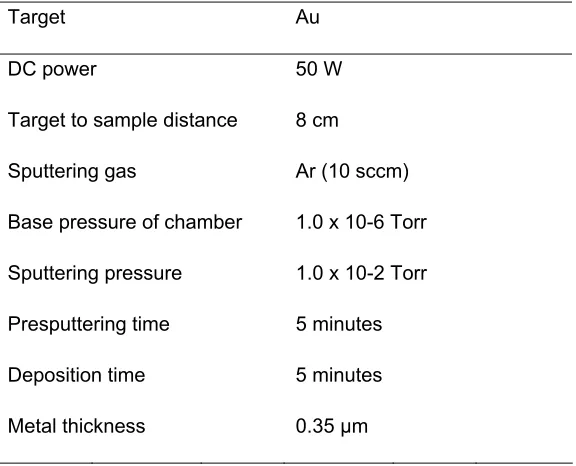
Table 2.1.3.2: Deposition conditions for Au (top electrode) sputtering
Target Au
DC power 50 W
Target to sample distance 8 cm
Sputtering gas Ar (10 sccm)
Base pressure of chamber 1.0 x 10⁻⁶ Torr
Sputtering pressure 1.0 x 10⁻² Torr
Presputtering time 5 minutes
Deposition time 5 minutes
Metal thickness 0.35 μm
Experiments where tantalum was used an adhesion layer were also done using the same deposition chamber.
2.2 Capacitor Fabrication
gaps were over-etched), and Cr-Au gap capacitors were also made with the BST dielectric that showed increased breakdown strengths.
2.3 Failure Testing
A Keithley 237 High Voltage Source Measurement Unit was used to submit capacitors to a ramping DC bias as shown in figure 2.3.1. The PC program Lab View was utilized to ramp all tested capacitors from 0 to 110 V in 1 V steps (each step takes one second), while current was monitored and graphically presented to observe if breakdown occurred. Current restrictions, which were available through Lab View, were necessary after it was determined in initial studies that we were unable to trace the root or causes of the failure. A third of the 225 capacitors were initially placed under the DC bias with the remaining gap capacitors available for testing later. Exposures to humidity, temperature, light, as well as the composition of the air where the testing took place were not controlled during experimentation.
2.4 Breakdown Statistics
As mentioned already, appropriate statistical methods were implored to analyze the incredible amounts of data collected from breakdown testing. These statistical methods can also be used to test a variety of variables and their relationship to breakdown strengths. The comparisons that were undertaken included testing capacitors with and without the presence of the BST dielectric, etching rather doing lift-off in acetone (without BST), the addition of the tantalum adhesion layer underneath the silver top electrode, varying substrate materials of sapphire and HRS, and finally Cr-Au capacitors.
The first variable that was analyzed using breakdown statistics was whether capacitors showed better breakdown strengths with or without the BST dielectric. Figure 2.4.1 shows data for 2 μm wide gaps with and without BST.
0 . 0 1 0 . 1 1
0 0 . 1 0 . 2 0 . 3 0 . 4 0 . 5
N o B S T
W i t h B S T
F (
X
i)
F i e l d ( M V / c m )
The first thing that is apparent when analyzing this data is the noticeable difference in breakdown strengths between when the dielectric is in use and when it is not. Capacitors with the BST dielectric do show markedly improved breakdown strengths as shown by the fact that the data is shifted slightly down and to the right in Figure 2.4.1. BST smoothes out the substrate’s roughness, which leads us to believe that surface roughness is an important factor in failure. Also, another interesting note is shown in how at low breakdown fields, the breakdown strength tends to be somewhat similar, which leads us to propose breakdown is being caused by a similar mechanism irregardless of the presence of BST.
0 . 0 1 0 . 1 1
0 0 . 0 5 0 . 1 0 . 1 5 0 . 2 0 . 2 5 0 . 3
L i f t - o f f p r o c e s s E t c h i n g p r o c e s s
F (Xi
)
F i e l d ( M V / c m )
Figure 2.4.2: Comparison of the cumulative probability of 4 micron Ag gap capacitors patterning processes
completed, the capacitors were found to be completely and utterly destroyed due to low the breakdown strengths (possibly from poor adhesion), and partially due to not using current limits. Therefore, the determination was made that silver had acceptable adhesion with the alumina substrates in this experiment.
0 .0 1 0 .1 1
0 0 .1 0 . 2 0 .3 0 .4 0 .5
N o a d h e s io n la y e r
T a a d h e s io n la y e r
F(
X
i)
F ie ld (M V / c m )
Figure 2.4.3: Experimental data comparing the cumulative probability of breakdown for 2
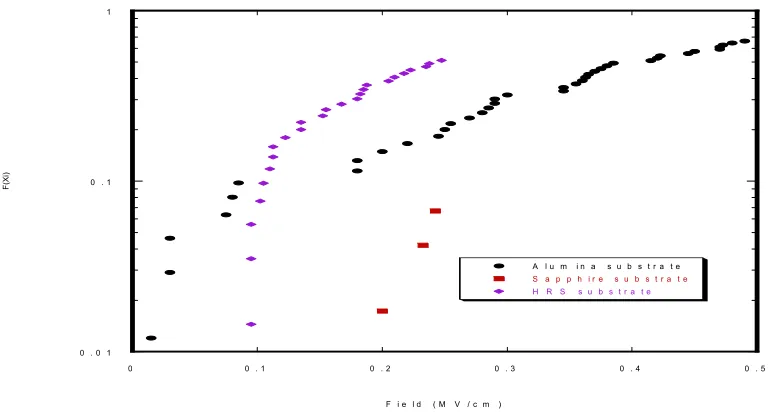
The next experiment undertaken was to study the breakdown statistics from testing capacitors on varying substrates to further investigate the effects of surface roughness. Sapphire, although expensive, is single crystal alumina and shows remarkable breakdown strengths as shown in figure 2.4.4. The availability of sapphire also presented problems; however, sapphire was the most superior substrate studied in regards to breakdown strengths. High-resistivity silicon (HRS) was another substrate that was considered for tunable filters. Figure 2.4.4 shows good breakdown strengths for capacitors on HRS at low voltages; however, capacitors on alumina substrates showed improved breakdown strengths at higher fields. Tunable filters were fabricated on both substrates, and their tunability was analyzed.
0 . 0 1 0 . 1 1
0 0 . 1 0 . 2 0 . 3 0 . 4 0 . 5
A l u m i n a s u b s t r a t e
S a p p h i r e s u b s t r a t e
H R S s u b s t r a t e
F(
X
i)
F i e l d ( M V / c m )
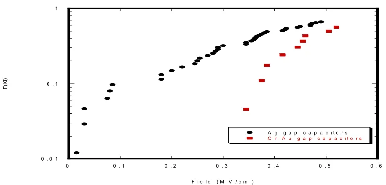
After determining the limitations of silver (see section 2.5 for a discussion silver electromigration) for the top electrode, other metals were necessitated for not only improved breakdown strengths, but also enhanced tunability. It was determined that gold could be used as the top electrode material (since Au has been widely used), but that it was necessary to also use chromium as the adhesion layer, since there were adhesion problems with gold on alumina. In figure 2.4.5, 2 μm Cr-Au gap capacitors show superior breakdown strengths to silver gap capacitors on alumina substrates with BST. The decision was then made to move on from silver as an electrode material for our tunable filters and begin using Cr-Au capacitors instead.
0 . 0 1 0 . 1 1
0 0 . 1 0 . 2 0 . 3 0 . 4 0 . 5 0 . 6
A g g a p c a p a c i t o r s C r - A u g a p c a p a c i t o r s
F(
X
i)
F i e l d ( M V / c m )
2.5 Methods for Determining Causes of Breakdown and Electromigration Experiments
As shown from the data above, Ag gap capacitors, regardless of BST deposition, show severe limits once an applied bias is placed on them. Some of the mechanisms previously mentioned as to causes of breakdown include but are not limited to dust, defects, and electromigration. An experiment was devised so as to explore the possibility of electromigration taking place with silver capacitors. This experiment required visual recognition of the occurrence of electromigration through the use of a scanning electron microscope.
Next, SEM images and energy dispersive x-ray spectroscopy (EDS) line and point scans were then taken again of the 25 capacitors that were placed under bias. In figure 2.5.1 we see an after image of a capacitor that failed after approximately 42 minutes of applied bias, and the cause of failure shown in a close-up on the right as a silver electro-migrated wire as pointed out by the arrow. An EDS line scan was performed on the gap as shown in figure 2.5.2 also confirms the existence of silver in the gap by the increase in silver concentration at the location of the wire. Lastly, an EDS point scan was completed to completely verify the presence of silver in the gap as shown in figure 2.5.3.
Figure 2.5.2: EDS line scan showing the presence of an electro-migrated silver wire inside the gap
Chapter 3
Chapter 3 corresponds to a manuscript that was submitted to the Journal of IEEE Ultrasonics, Ferroelectrics, and Frequency Control Society (UFFC). The manuscript is currently under review.
Mechanisms and statistics of silver gap capacitor failure on alumina substrates
James Kupferschmidt, Peter G. Lam, *Zhiping Zheng, *Vrinda Haridasan, Angus I. Kingon,
*Michael B. Steer, and Jon-Paul Maria
North Carolina State University, Departments of Materials Science and Engineering and
3.1 Abstract
Numerous modern-day communication devices utilize tunable filters using ferroelectric varactors to tune over a wide range of frequencies. The varactors consist of capacitors in series employing the dielectric as the basis for their tunability. Reliability of the capacitors composing the varactors is a significant concern, especially with our current use of silver gap capacitors. Banks of silver gap capacitors were fabricated using photolithography techniques and DC sputtering on alumina substrates with and without the presence of the BST dielectric. Capacitors were then placed under a ramping DC bias to observe if failure would occur. Capacitors employing the BST dielectric showed improved breakdown strengths owing mainly to the elimination of alumina’s surface roughness when the thin-film is deposited on top of the rough substrate surface. Explorations into the mechanisms of breakdown are also delved into, with silver electromigration confirmed as a major mechanism producing breakdown.
3.2 Introduction
A wide array of modern communication devices necessitate tunable filters with ferroelectric varactors designed for broad ranges of frequencies. Microwave systems, such as antennas, 1 phase shifters 2, and voltage-controlled oscillators 3 have incorporated the use of thin-film Barium Strontium Titanate, BaxSr1-xTiO3 or BST as a dielectric material. BST, a
tunable by regulating voltage to obtain varying capacitance values at room temperature. The ability to function over an extensive range of frequencies allows for compactness rather than large numbers of devices functioning only at a specific frequency. Tuning occurs at the extremely fast speeds of nanoseconds, and the technology is also inexpensive. Tunable filters have shown to exhibit low losses 4-6 leading to a high quality factor 7 and possess the ability for straightforward integration into already existing technologies. BST is known to possess a high dielectric constant, which allows for device flexibility and efficiency, and is deposited using optimal conditions by radio frequency (RF) magnetron sputtering. Ferroelectric BST varactors with capacitors in series have been successfully used in numerous tunable filters 4-8.
outstanding advantages as a substrate for frequency-agile devices. They are available at relatively low cost and exhibit low loss tangent (~10-4) in the microwave range. Alumina also possesses a similar coefficient of thermal expansion to BST while having a low dielectric in the high frequency range. Large numbers of gap capacitors with varying gap widths and lengths were fabricated on alumina substrates with and without the presence of BST and then placed under ramping DC bias. Capacitors which experienced failure were then analyzed with the appropriate statistical methods. Mechanisms for breakdown of the capacitors are considered, and include but are not limited to surface roughness, electromigration, contamination, and device geometry. The theory behind capacitor failure is also considered and applied to our particular area of study.
3.3 Experimental Procedure
Next, another set of capacitor samples were prepared by completing lithography after deposition of the dielectric. A stoichiometric BST target, with a Ba/Sr ratio of 70/30 respectively (this ratio is favorable for tunability of filters and loss tangent), was employed by the use of RF magnetron sputtering. Inside the sputtering chamber, the substrate platform is heated to 300ºC, and sputtering can take place once the chamber reaches 5x10⁻⁵ Torr. Pure flowing argon was allowed to flow into the chamber at a pressure of 1x10⁻² Torr for when sputtering occurs. The sputtering took place for 60 minutes on a rotating platform to give a thin film thickness of 0.5 μm. After deposition of BST is complete, the substrate is annealed in air at 900ºC for 20 hours to allow for complete crystallization and densification of the dielectric.
Metallization was accomplished with silver by the use of a DC magnetron sputtering system at room temperature. Silver metal is exploited due to its high electrical conductivity as well as the low losses in signals for filters. The chamber was evacuated to a pressure of 5x10⁻⁵ Torr, and the deposition of Ag takes ten minutes at 20 mTorr of argon to obtain a thickness of 350 nm. This pressure allows for good adhesion and low impurities. Patterning was then accomplished by lift-off in an acetone solution over a brief period of time. After lift-off is completed, the samples are dried using nitrogen, and the gaps are examined with a microscope to verify the features were fully developed.
taking place, the current is recorded and shown on the PC program Lab View in graphical form with voltage on the horizontal axis and current on the vertical axis. This program also permitted for the restriction of current for when later studies were undertaken to investigate the sources of breakdown. Each substrate consisted of approximately 225 capacitors with equal numbers of two, three, four, and five micron gaps with widths ranging from 100 to 750 microns. One-third of the capacitors were initially placed under ramping DC bias with the remaining capacitors saved for further testing and other data analysis. No attempts were made to control the exposure to light, temperature, humidity, or the composition of the air in this portion of the experiment.
Interpretation of breakdown data was undertaken using Weibull statistics methodology due to the mechanism of failure being field emission. Capacitors which failed were ranked by breakdown voltage from lowest to highest and thus assigned a corresponding ranking. The electric field was calculated by dividing the breakdown voltage by the proper gap length. Cumulative probability was determined by using the Bernard median rank equation 10:
4 . 0 3 . 0 ) ( + − = n i x
F i (1)
3.4 Results and Discussion
3.4.1. Ag Gap Capacitor Failure on Alumina Substrates Without BST
A typical I-V curve for a silver metal-insulator-metal capacitor failure is shown in figure 3.4.1.1. The locations of the soft breakdown and complete breakdown are shown to decipher how breakdown voltage is determined via graphical methods. Figure 3.4.1.2 shows the log-normal cumulative probability of the breakdown field for the samples without BST. Breakdown of these capacitors occurred at exceedingly low fields. Numerous capacitors on the samples without the dielectric failed at extremely low voltages, which necessitated current restrictions so as not to completely destroy all evidence as to the source of the breakdown.
Soft breakdown Complete breakdown
0 . 0 1 0 . 1 1
0 0 . 1 0 . 2 0 . 3 0 . 4 0 . 5
2 m i c r o n 3 m i c r o n 4 m i c r o n 5 m i c r o n
F (Xi
)
F i e l d ( M V / c m )
Figure 3.4.1.2: Cumulative probability of breakdown field for Ag MIM capacitors on alumina with no BST
Figure 3.4.1.3: SEM image showing a 4-micron silver MIM capacitor gap on alumina with no BST without current limits after dc bias has been applied
3.4.2. BST Incorporated as a Dielectric for Ag Gap Capacitors
extremely rough and contain countless scratches and cracks making photolithography complex. When the BST is deposited on top of the substrates, the roughness of the alumina is lessened by smoothing out the jaggedness and cracks on the surface.
0 . 0 1 0 . 1 1
0 0 . 1 0 . 2 0 . 3 0 . 4 0 . 5
2 m i c r o n 3 m i c r o n 4 m i c r o n 5 m i c r o n
F (X
i)
F i e l d ( M V / c m )
Figure 3.4.2.1: Cumulative probability of breakdown field for silver gap capacitors on alumina with BST
sources of breakdown. The next logical step would be to correlate the different slopes to the mechanism of failure.
0 .0 1 0 .1 1
0 0 .1 0 .2 0 .3 0 .4 0 .5
N o B S T
W ith B S T
F (Xi
)
F ie ld (M V / c m )
Figure 3.4.2.2: Cumulative probability of breakdown field for 2-micron wide gap Ag capacitors on alumina with and without BST
the rough surface on which the capacitor is situated, where the rough surface leads to field amplification between the contacts. In figure 3.4.2.3, the failure occurs more towards the edge of the capacitor because of increased strength due to the smoother surface on which the electrodes are fashioned, which in-turn promotes better adhesion and thus increased breakdown strength. No current limits were utilized on the sample in figure 3.4.2.3, so a direct comparison of the two samples can occur. Another interesting note regarding figure 3.4.2.3 is the image shows cracking of the dielectric layer, signifying that the dielectric is also serving to enhance the breakdown strength.
3.5 Discussion
As has now been presented, high breakdown fields tend to occur at edges on the capacitors and also are not likely to destroy the gap in an explosive manner as shown in figure 3.4.2.3. Low breakdown fields have a tendency to occur in the weak spot away from the edges and also tend to obliterate the gap much wider than high breakdown fields do as exhibited in figure 3.4.1.3. One explanation for the occurrence of this phenomenon having already been discussed is substrate roughness, which leads to field amplification between the electrodes due to their close proximities.
To further study the suspected effect of electromigration, a short experiment was conducted to visually identify the occurrence of electromigration. Another sample of capacitors was fabricated on an alumina substrate without the dielectric. Before placing a DC bias to these capacitors, SEM images of the capacitor gaps were taken to serve as a reference, since the Pt layer was now unnecessary. Approximately 25 capacitors were placed under an applied bias of 15 V to initiate diffusion until failure occurred. The voltage was applied to capacitors with the narrowest widths (around 105 microns) over the entire range of gaps (2 to 5 microns), so as minimize the number of images needed across the entire length of the gap and because narrow width capacitors in theory should be the most robust. Of the 25 capacitors tested, the average time to breakdown was roughly one hour. SEM images were then taken again after failure across the entire length of the gap to verify the existence of electromigration. Figure 3.5.1 shows a frequently common set of images taken before and after applied voltage on the same location for the same capacitor, which verifies the existence of electromigration of silver in the gaps leading to a shorting-out of the capacitor.
In relation to the existing breakdown theory, Paschen’s Law is found to be inadequate for the breakdown results from this study. Paschen’s Law, in the form of V = f (pd), has only been show to be reliable for gaps of 10 μm or more 14. The mechanism behind Paschen’s Law is given by Townsend’s electron avalanche theory in which gas ionization takes place leading to an especially small number of free electrons, which then increase in velocity due to strong electric field, giving rise to electrical conduction through a gas by avalanche multiplication. This mechanism has been found not to be applicable for gaps of less than 6
μm 15. Also, Paschen’s Law is related to humidity, which was not controlled in this experiment. An interesting side-note: Paschen’s Law was developed for the geometry of spheres and not for parallel-plate metal contacts with micron spacings, which can partially help to explain the deviations in fields. There is literature attempting to explain the breakdown of incredibly narrow gaps in the low micron-range as due to field emission electrons from the cathode contact initiating electron avalanche. Since the field in the gap is quite large, electrons can tunnel through the deformed surface potential barrier 14, so electrons actually reach the conduction band of the insulator.
3.6 Conclusions
current limitations were not used during the ramping DC bias; however, after visual examination of the destruction, the necessity for current restrictions was determined to better understand the failure, since higher current leads to higher power and ultimately more damage. Data, along with explanations are provided showing improvements for capacitors when the BST dielectric is deposited prior to photolithography. The explanation behind this effect is given due to surface roughness effects. Capacitors with low breakdown strengths are likely to destroy the gap in a very violent manner, while capacitors with high breakdown strengths tend to occur out along the edges of the capacitors and do not produce as much damage. The mechanism of electromigration is demonstrated to be a factor in the breakdown of these capacitors. A simple experiment was carried out to visually prove silver electromigration is occurring and is a major cause for failure. The breakdown fields were also revealed not to follow Paschen’s Law. There are several reasons for the deviation from this theory, including humidity and geometry affects.
3.7 References
1 L. Sengupta, “Novel ferroelectric materials for phased array antennas,” Ultrasonics,
Ferroelectrics and Frequency Control, IEEE Transactions on, vol. 44, 1997, pp.
792-797.
2 Yu Liu et al., “BaSrTiO3 interdigitated capacitors for distributed phase shifter
applications,” Microwave and Guided Wave Letters, IEEE, vol. 10, 2000, pp. 448-450.
3 A. Victor et al., "A Voltage Controlled Oscillator Using Barium Strontium Titanate
4 A. Tombak et al., “Voltage-controlled RF filters employing thin-film
barium-strontium-titanate tunable capacitors,” Microwave Theory and Techniques, IEEE Transactions
Microwave Theory and Techniques, vol. 51, 2003, pp. 462-467.
5 J. Nath et al., “An electronically tunable microstrip bandpass filter using thin-film
Barium-Strontium-Titanate (BST) varactors,” Microwave Theory and Techniques, IEEE
Transactions on, vol. 53, 2005, pp. 2707-2712.
6 J. Nath et al., “Discrete Barium Strontium Titanate (BST) Thin-Film Interdigital
Varactors on Alumina: Design, Fabrication, Characterization, and Applications” IEEE
MTT-S Int. Microwave Symp., June 2006.
7 D. Ghosh et al., “Tunable high Q interdigitated (Ba, Sr)TiO
3 capacitors fabricated on low
cost substrates with copper metallization,” Thin Solid Films, 496 [2], 669 (2006).
8 P. Lam et al., “The Impact of Metallization Thickness and Geometry for X-Band Tunable
Microwave Filters,” IEEE UFFC, 2008.
9 E. Hourdakis et al., “Submicron gap capacitor for measurement of breakdown voltage in
air,” Review of Scientific Instruments, 77, 034702 (2006).
10 J.C. Fothergill, “Estimating the Cumulative Probability of Failure Data Points to be
Plotted on Weibull and other Probability Paper,” IEEE Transactions on Electrical
Insulation, vol. 25 No. 3, 1990, pp. 489-492.
11 Hauder et al., “Scaling properties and electromigration resistance of sputtered Ag
metallization lines,” Applied Physics Letters, vol. 78, 6 (2001).
12 P.S. Ho and H.B. Huntingdon, “Electromigration and Void Observation in Silver,” J.
Phys. Chem. Solids, vol. 27, 1966, pp. 1319-1329.
13 S. Krumbien, “Metallic Electromigration Phenomena,” IEEE Holm Conference on
Electrical Contacts, 1987.
14 A. Wallash and L. Levit, “Electrical breakdown and ESD phenomena for devise with
nanometer-to-micron gaps,” Proc. SPIE, 2003, 87.
15 P.G. Slade and E.D. Taylor, “Electrical Breakdown in Atmospheric Air Between Closely
Spaced (0.2 μm-40 μm) Electrical Contacts,” IEEE Trans. Compon. Packag. Technol.,
Chapter 4: Conclusions
The work offered in this thesis was beneficial in contributing to our knowledge and understanding of producing improved tunable filters for communication systems. Other technologies also incorporate the use of capacitors with small gap spacings upon which this research is relevant. This thesis also deals with the statistical analysis involved in the organization of the breakdown data to determine the critical variables leading to increases in breakdown strengths.
• Silver gap capacitors with the BST dielectric show much improved breakdown strengths over capacitors where the dielectric is not present. We propose that this effect is due to the surface roughness of the alumina, which can be reduced with the deposition of the BST dielectric.
• The existence of the electromigration process was visually confirmed and verified using SEM and EDS analysis for silver gap capacitors. The next step would be to actually fail some capacitors while performing SEM analysis to observe the breakdown process itself. • Once the existence of silver electromigration had been proved as one of the leading mechanisms of breakdown, it became necessary to explore other combinations of metals for use in our electrodes, as well as substrates. Using the appropriate Weibull statistical examination, Cr-Au gap capacitors were shown to have much improved breakdown strengths, and sapphire substrates showed similar results as well.
References
1 T. Ayguavives, A. Tombak, J.P. Maria, G.T. Stauf, C. Ragaglia, J. Roeder, A. Martazawi,
and A.I. Kingon, “Physical properties of (Bar,Sr)TiO3 thin films used for integrated
capacitors in microwave applications”, IEEE ISAF 2000, Vols. I and II, pp. 365 – 368,
(2001)
2 A. Tombak, J.P. Maria, F. Ayguavivies, Z. Jin, G.T. Stauf, A.I. Kingon, and A.
Mortazawi, “Tunable Barium Strontium Titanate Thin Film Capacitors for RF and
Microwave Applications”, IEEE Micro. and Wireless Comps. Letters, Vol. 12, 1, (2002)
3 C.B. Parker, J.P. Maria, and A.I. Kingon, “Temperature and thickness dependent
permittivity of (Ba,Sr)TiO3 thin films”, App. Phys. Letters, Vol. 81, 2, (2002)
4 Z. Jin, A. Tombak, J.P. Maria, B. Boyette, G.T. Stauf, A.I. Kingon, and A. Mortazawi,
“Microwave Characterization of Thin Film BST Material Using a Simple Measurement
Technique”, IEEE MTT-S Dig., Vols. 1-3, pp. 1201-1204, (2002)
5 M.E. Lines and A.M. Glass, “Principles and Applications of Ferroelectrics and Related
Materials”, (Clarendon, Oxford, 1977), p. 71
6 P. Padmini, T.R. Taylor, M.J. Lefervre, A.S. Nagra, R.A. York, and J.S. Speck,
“Realization of high tunability barium strontium titanate thin films by rf magnetron
sputtering”, Appl. Phys. Lett., 75, pp. 3186-3188, (1999)
7 K. Bethe, and F. Welz, “Preparation and properties of (Ba, Sr) TiO
3 single crystals”,
8 A.I. Kingon, J.P. Maria, and S.K. Streiffer, “Alternative dielectrics to silicon dioxide for
memory and logic devices”, Nature, Vol. 406, pp. 1032-1038, (2000)
9 S.K. Streiffer, C. Basceri, C.B. Parker, S.E. Lash, and A.I. Kingon, “Ferroelectricity in
thin films: The dielectric response of fiber-textured (BaxSr1-x)Ti1+yO3+z thin films grown
by chemical vapor deposition”, Journal of Appl. Phys., Vol. 86, 8, (1999)
10 D.J. Taylor, “Handbook of Thin Film Devices”, 5, Academic Press, USA, (2000)
11 B. Noren, “Thin Film Barium Strontium Titanate (BST) for a New Class of Tunable RF
Components”, Microwave Journal, vol. 47, pp. 210-220, (2004)
12 E.R. Brown, “RF-MEMS switches for reconfigurable integrated circuits”, IEEE Trans.
Microw. Theory Tech., vol. 46, pp. 1868-1880, (1998)
13 A. Victor, J. Nath, D. Ghosh, B. Boyette, J.P. Maria, M.B. Steer, A.I. Kingon, and G.T.
Stauf, “A Voltage Controlled Oscillator Using Barium Strontium Titanate (BST) Thin
Film Varactor”, IEE Proc.-Microw. Antennas Propag., Vol. 153, 1, (2006)
14 A. Victor, J. Nath, D. Ghosh, B. Boyette, J.P. Maria, M.B. Steer, A.I. Kingon, and G.T.
Stauf, “Noise characteristics of an oscillator with barium strontium titanate (BST)
varactor”, IEE Proc.-Microw. Antennas Propag., Vol. 153, 1, (2006)
15 Y. Liu, A. Nagra, E.G. Erker, P. Periaswamy, T.R. Taylor, J. Speck, and R.A. York,
“BaSrTiO3 Interdigitated Capacitors for Distributed Phase Shifter Applications”, IEEE
16 B. Acikel, T.R. Taylor, P.J. Hansen, J.S. Speck, and R.A. York, “A New High
Performance Phase Shifter using BaxSr1-xTiO3 Thin Films”, IEEE Microw. and Wireless
Comps. Lett., vol. 12, 7, (2002)
17 A. Tombak et al., “Voltage-controlled RF filters employing thin-film barium-strontium
titanate tunable capacitors,” Microwave Theory and Techniques, IEEE Transactions
Microwave Theory and Techniques, vol. 51, 2003, pp. 462-467
18 J. Nath et al., “An electronically tunable microstrip bandpass filter using thin-film
Barium-Strontium-Titanate (BST) varactors,” Microwave Theory and Techniques, IEEE
Transactions on, vol. 53, 2005, pp. 2707-2712
19 J. Nath et al., “Discrete Barium Strontium Titanate (BST) Thin-Film Interdigital
Varactors on Alumina: Design, Fabrication, Characterization, and Applications” IEEE
MTT-S Int. Microwave Symp., June 2006
20 D. Ghosh et al., “Tunable high Q interdigitated (Ba, Sr)TiO
3 capacitors fabricated on low
cost substrates with copper metallization,” Thin Solid Films, 496 [2], 669 (2006) 21 J. Xu, W. Menesklou, and E.I. Tiffee, “Processing and properties of BST thin films for
tunable microwave devices”, J. Eur. Ceram. Soc., 24, pp. 1735-1739, (2004)
22 D. Kim, Y. Choi, M. Ahn, M.G. Allen, J.S. Kenney, and P. Marry, “2.4 GHz Continously
Variable Ferroelectric Phase Shifters Using All-Pass Networks”, IEEE Microwave
23 J.P. Maria, B.A. Boyette, A.I. Kingon, C. Ragaglia, G. Stauf, “Low loss tungsten-based
electrode technology for microwave frequency BST varactors”, J. Electroceram., 14, pp.
75-81, (2005)
24 Leonard B. Loeb, “Streamer Breakdown and Sparking Thresholds”, Phys. Review, vol.
81, 2, p. 287, (1950)
25 K. Hasebe and K. Yamamoto, “Streamer Theory and the Value of α/ρ”, Phys. Review,
vol. 99, 4, pp. 1331-1332, (1955)
26 L.H. Germer, “Electrical Breakdown between Close Electrodes in Air”, Journal of App.
Phys., vol. 30, 1, (1959)
27 R.M. Secareanu, M. Jones, M. Sadd, B. White, P. Maniar, “Circuit challenges and
proposed solutions targeting nanometer technologies”, IEEE International ASIC/SOC
Conf., pp. 325-329, (2001)
28 S.W. Janson, “Micro/nanotechnology for the satellite world”, SPIE, vol. 4981, pp.
95-106, (2003)
29 S. Knight, R. Dixson, R.L. Jones, E.K. Lin, N.G. Orji, R. Silver, J.S. Villarrubia, A.E.
Vladar, and W.L. Wu, “Advanced metrology needs for nanoelectronics lithography”, Comptes Rendus Physique, vol. 7, 8, pp. 931-941, (2006)
30 P.G. Slade and E.D. Taylor, “Electrical Breakdown in Atmospheric Air Between Closely
Spaced (0.2 μm-40μm) Electrical Contacts”, IEEE Trans. on Comps. and Packag. Tech.,
31 Yu-Tzu Chiu, S.K. Moore, “Faults & Failures: Leaking capacitors muck up
motherboards” , IEEE Spectrum, 40, (2), pp. 16–17, (2003)
32 M. Pecht, T. Sanjay “Bogus! Electronic manufacturing and consumers confront a rising
tide of counterfeit electronics” , IEEE Spectrum, 43, (5), pp. 37–46, (2006)
33 F. Paschen, 1889 Wied. Ann 37, pp. 69-96
34 E. Hourdakis, B.J. Simonds, and N.M. Zimmerman, “Submicron gap capacitor for
measurement of breakdown voltage in air”, Rev. of Sci. Instr. 77, (2006)
35 A. Wallash, and L. Levit, “Electrical breakdown and ESD phenomena for devices with
nanometer-to-microngaps”, Proc. SPIE, 87, (2003)
36 J.S. Townsend, “Motion of Electrons in Gases”, J. Franklin Inst., vol. 200, pp. 563-590,
(1925)
37 F. Gomer, “Field Emission and Field Ionization,” Harvard University Press, (1961) 38 Robert Stratton, “Theory of Field Emission from Semiconductors”, Physical Review, vol.
125, 1, (1962)
39 J.C. Fothergill, “Estimating the Cumulative Probability of Failure Data Points to be
Plotted on Weibull and other Probability Paper”, IEEE Trans. on Elec. Insulation, vol.
25, 3, (1990)
40 P.S. Ho and H.B. Huntingdon, “Electromigration and Void Observation in Silver,” J.
Phys. Chem. Solids, vol. 27, 1966, pp. 1319-1329
41 S. Krumbien, “Metallic Electromigration Phenomena,” IEEE Holm Conference on
42 M. Hauder, J. Gstottner, W. Hansch, and D. Schmitt-Landsiedel, “Scaling properties and
electromigration resistance of sputtered Ag metallization lines”, Appl. Phys. Lett., vol.