Observation of System Performance for Lag
Compensation from Universal Design Method
R. Kiranmayi
Associate Professor, Department of EEE, JNTUHCEH, Hyderabad, India
ABSTRACT: Compensators are corrective sub systems to force the chosen plant to meet the given specifications. Their purpose is to compensate for the deficiency in the performance of the plant. The Universal chart facilitates accurate compensators design and also satisfies the system specifications in frequency domain and steady state error. This paper shows the derivation of lead compensator from universal design which is useful for different time domains. The design is carried out with the approach of frequency domain specification. The improved time domain specifications are observed from the resulting graphs.
KEYWORDS: Lag compensators, Universal design chart, Bode plots, Continuous systems, overshoot.
I. INTRODUCTION
Control system design via the frequency domain and specifically using the Bode plots has been well established. Various Bode design charts and formulae were developed for the most common continuous-time and discrete-time compensators by Yeung. This paper enhances, emphasis and shows the possibility to derive lag compensators from a single universal design which also facilitates the design of many of other conventional compensators. The system response and the stability of the system are shown graphically to emphasize the improvement in the performance of the system. In the sequel, first the essence of the design method is presented, then formulae for the compensators are given which are used in conjunction with the universal design and then the plots and graphs are drawn for uncompensated and compensated systems.
II. DESIGN METHOD PRINCIPLE
To illustrate the basic idea of the compensator design, consider a plant with the frequency response Gp(jω). A
compensator Gc(jω) is to be inserted in series with the plant so that a desired value for the phase margin (PM) or gain
margin (GM) is obtained.
By the definitions of PM and GM, for the case of PM
|G
c(j
ω
g)G
p(j
ω
g)|
db= 0
(G
c(j
ω
g)G
p(j
ω
g)) = PM – 180
o(1)
and for the case of GM
|Gc(jωph)Gp(jωph)|db = –GM
(Gc(jωph)Gp(jωph)) = – 180 o(2)
Where | |db denotes the 20log decibels of the magnitude, | denotes the phase angle. ωg is the gain crossover frequency
and ωph is the phase crossover frequency.
Equations (1) and (2), respectively, can be rewritten as
|Gc(jωg)|db = – |Gp(jωg)|db
(Gc(jωg) = –
Gp(jωg) + PM – 180o (3)and
|Gc(jωph)|db = –|Gp(jωph)|db = – GM
(Gc(jωph) = –
Gp(jωph) – 180o (4)The left-hand sides of (3) and (4) depend only on the compensator. It can also be shown that for all the compensators frequency response can be normalized into the standard form.
(1 + jB)
Gc(A, B) = ––––––– (5)
(1 + jA)
where A, B and C are in general functions of the frequency and compensator parameters. Let (1 + jB)
Gc(A, B) = ––––––– (6)
(1 + jA) so that
Gc(jω) = CGc(A, B) (7)
Substitution of (7) into (3) at ω = ωg gives
| Gc(A, B)|db = – |CGp(jω)|db
Gc(A, B) = –
(CGp(jω)) + PM – 180o (8)Substitution of (7) into (4) at ω = ωph gives
|Gc(A, B)|db = – |CGp(jω)|db – GM
Gc(A, B) = –
(CGp(jω)) – 180o (9)If C is known, then the right-hand sides of (8) or (9) can be plotted as a plant curve. Intersection of plant curve with the appropriate curve on the universal design chart will yield the A and B values which in turn will give the compensator parameter values.
III. PLOTTING OF UNIVERSAL DESIGN CHART
Standard form of compensator in frequency domain is
(1 + jB) Gc(A, B) = –––––––
(1 + jA) The above equation in rectangular form is given as
(1 + jB)
Gc(jω) = C –––––––
(1 + jA)
(1 + AB) (B – A) = C –––––––– + j C ––––––
(1 + A2) (1 + A2) This is the basic equation to plot the universal design chart. The plotting of universal design chart is done in two steps.
1. Plotting of the A – curves. 2. Plotting of the B – curves.
PLOTTING OF A CURVES:
A curves are plotted using basic equation by varying the values of A for the fixed value of B. The A curve is drawn with the magnitude on Y-axis and the phase angle on X- axis. This curve is known as A curve. To draw more A curves above procedure can be repeated for different values of A.
PLOTTING OF B CURVES:
B curves are plotted using basic equation by varying the values of B for the fixed value of A. The magnitude is taken on Y- axis and the phase angle is taken on X- axis. This curve is known as B curve. Many values of A gives many B curves. To draw more B curves above procedure can be repeated for different B values.
The universal design indicates the plotting of A and B curves on same plane which results in universal design chart.
IV. TRANSFORMATION OF PHASE- LAG COMPENSATOR INTO STANDARD FORM
The frequency response of the phase-lag compensator is equated to the standard form
(1 + jB) (1 + jTω)
(1 + jA) (1 + jβTω)
yielding
C = K (11)
β = A/B (12)
T = β/ω (13)
Frequency is to be specified as either ωgor ωph.
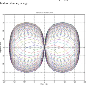
Fig. 1 General Universal Design Chart
V. ILLUSTRATIVE EXAMPLE
Following illustrates the designing of phase- lag compensator to satisfy the following specifications: (i) The phase margin of the system = 48 degree
(ii) Velocity error constant Kv = 2
(iii) The gain crossover frequency of the system must be less than 2.5 rad/sec for the system Gp(S) = 3 / S (S2 +4 S + 5), H(S) = 1.
Method: The given plant transfer function is
3 Gp(S) = ––––––
S(S2 +4 S + 5)
The transfer function of phase lag compensator is
K (1+ S T) Gc(S) = –––––––––––
(1+ SβT)
Transformation of compensator into standard form yields
C = K (K is determined from steady state requirements)
β = A / B
From the data , Kv = 2 and
Lt
Kv = S (Gp(S) Gc(S))
S→ 0
Lt 3 K(1 + S T )
Kv = S –––––– ––––––––––– = 2
S→0 S(S2+4S+5) ( 1 + SβT)
Therefore K = 3.33 and C = 3.33
So
Gp(S) = 3/S(S2+4S+5)
Gp(jw) = –12/(25 +6 ω2+ ω4) – J (15 / (ω – 3ω)) / (25+6ω2+ ω4)
X = –12 / (25 +6 ω2+ ω4)
Y = (15 / (ω – 3ω)) / (25+6ω2+ ω4)
Z = X – j Y
|Gp(jω)| db = 20 log(abs(Z))
|Gc(jω)| db = |C Gp(jω)| db
Gp(jω) = –90 – tan-1(4ω/(5 – ω2)) = –90 – (180 – tan-1(4ω/(5 – ω2)))
Gc(A,B) = –
CGp(jω) + PM – 180= – (–90 – (tan –1(4ω / (5 – ω2)))) + PM – 180
= 90 + (180 + tan-1(4ω / (5 – ω2))) + 132
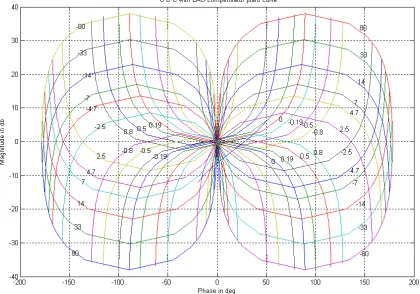
Using above equations plant curve is drawn on universal chart.
Fig. 2 Universal design chart with lag compensator plant curve
From above figure A, B values are 0.19 and 2.5. Therefore β = A / B =0.19 / 2.5 = 0.0760
With these β and T values compensator transfer function is 3.33(1+S) Gc(S) = ––––––––––
(1 + 0.0766 S)
Therefore the compensated system becomes
3 3.33(1+S) Gp(S)Gc(S) = –––––––– ––––––––
S(S2+4S+5) (1+0.0.076 S)
Fig.3 Bode plot of uncompensated system
Fig.5 Step response of the system
VI. CONCLUSIONS
This paper provides design of lag compensators using a universal chart which enables an efficient design of the most common compensators also. A method for lag compensator design is presented. It is based on the idea of normalizing compensator parameters so that a design chart can be generated once for all. A design example is carried through to illustrate the use of this design chart. The Bode plot and the steady state response are drawn. The coding is done in MATLAB. It can be observed from the plots that the desired phase margin is obtained and also the steady state response is improved. The method proves to take less time and iterations compared to conventional compensator design. The method involves less complexity. Simultaneous fulfillment of the specifications of gain margin, and gain crossover frequency can be achieved with accuracy.
VII. ACKNOWLEDGEMENTS
I acknowledge the almighty for his blessings and my family for their constant support and also my student for his contribution towards this work.
REFERENCES
[1] Kai Shing Yeung, Kuo Hsum Lee, “A Universal Design Chart for Linear Time-Invariant Continuous-Time and Discrete-Time Compensators” IEEE Trans. on Educ., Vol.43, No.3, pp.309-315, Aug. 2000.
[2] W.R.Wakel, “Bode compensator design,” IEEE Trans. Automat. Contr., Vol. AC-21, pp.771-773, Oct. 1976. [3] R. Kiranmayi, “Lead Compensators from Universal Design Method” IJAREEIE, Vol. 1, Issue 3, Sept. 2012.
[4] R. Kiranmayi, “Observation of System Performance for Lead Compensation from Universal Design Method” IJAREEIE, Vol. 1, Issue 4, Oct. 2012.
[5] R. Kiranmayi, “Lag Compensators from Universal Design Method” IJIRSET, Vol. 1, Issue 1, Nov. 2012.
[6] J.R.Mitchell, “Comments on bode compensator design,” IEEE Trans. Automat. Contri., vol. AC-22, pp.869-870, Oct.1977. [7] K.Q.Chaid, “Bode compensator design,” M.S. Thesis, Univ. Taxes, Arlingtion 1986.
[8] K.S.Yeung, K.Q.Chaid, “Bode design formulas for discrete compensators,” Electron. Lett., vol.22, no.24, Nov. 21, 1986.
[9] K.S.Yeung, K.Q.Chaid, and T.X.Dinh, “Bode design chart for continuous-time and discrete-time compensators” IEEE Trans. Educ., vol.38, pp252-257, Aug.1995.
[11] Ogata K.,“Modern control Engineering” Practice Hall of India,Pvt. Ltd., New Delhi, 1995. [12] D.R.Wilson, “Modern Practice in servo design” Pergmon Press, 1970.
[13] Benjamin C.Kuo, “Automatic control systems” Practice Hall of India, Pvt. Ltd., New Delhi, 1979.
BIOGRAPHY