Uncooled Carbon Microbolometer Imager
Thesis by
Matthieu Liger
In Partial Fulfillment of the Requirements
for the Degree of
Doctor of Philosophy
California Institute of Technology
Pasadena, California
2006
c
° 2006 Matthieu Liger
Acknowledgements
I will start by thanking my advisor, Yu-Chong Tai, first for giving me the opportunity
to study and work in the Caltech Micromachining Laboratory and for mentoring me. I only
wish I could be as creative and optimistic as he is.
There are other professors I want to thank. First, my sophomore-year physics teacher,
Val´erie Douay. If it wasn’t for her extremely well-taught and inspiring electromagnetism
class, I might not be here today. I am also thankful to the Professors who sat in my
candidacy committee and/or defense committee: Ali Hajimiri, Ellis Meng, Oskar Painter,
Demetri Psaltis, Axel Scherer, and Changhuei Yang.
Thanks to the “senior” labmates who taught me how to work around the lab, especially
Nick Pornsin-Sirirak, Yong Xu, Jun Xie, Tze-Jung Yao and Ellis Meng. I still cannot
believe I am now the senior guy in the lab. Thanks to my officemates Victor Shih and Qing
He for some great discussions and to the rest of the Caltech Micromachining lab: Damien
Rodger, Justin Boland, Ted Harder, Scott Miserendino, Angela Tooker, Siyang Zheng; the
great Tanya Owen for taking such good care of us and Trevor Roper for taking care of the
machines, some of which, being older than us, can be a handful. I also want to acknowledge
Professor Satoshi Konishi of Ritsumeikan University and Doctor Stacey Boland who made
some of the measurements presented in Chapter3.
Thanks to the Caltech staff in general for making Caltech such wonderful environment
for students; I am thinking especially of the people at the International Students Programs
office: Parandeh Kia, Jim Endrizzi and Tara Tram. To Linda Dozsa, Veronica Robles, and
Janet Couch from the electrical engineering department, to the staff of Red Door Cafe for
the thousands of double expressos I must have had there, and the Chandler pizza guys.
I thank the people without whom my years in graduate school would not have been
as pleasant. From the very first days of the international student orientation at Caltech:
Komijani, then later Hossein Hashemi, Sam Mandegaran, Nikoo Saber, Leila Setayeshgar,
Lisa Cowan, Roya Bahreini, Ivana Komunjer, Maxime Rattier, Fatemeh Jalayer, Eva Kanso,
Aaron Sorkin, and last but not least, Maryam Fazel. My roomates Olivier Delaire, Nicolas
Ponchaut, Frank Ducheneaux, and Pierre Moreels for tolerating me, even when I was asleep
on the couch.
Finally, I thank my parents who tried to deal with a kid who was more interested in
doing experiments in the basement than he was in doing his homework. As it turned out,
Abstract
The discovery of infrared radiation two centuries ago and the theory of blackbody
ra-diation one century later have given birth to the field of thermal imaging. Since then,
researchers have devised numerous ways to detect infrared radiation. From World War II
to the 1980s, semiconductor-based cooled photon detector arrays have reigned over the field
of thermal imaging. Albeit limited to expensive, bulky systems used for military
applica-tions due to their cooling requirement they have been . The emergence of micromachining
techniques in the 1980s however, have allowed for the development of uncooled, thermal
de-tector arrays. Uncooled systems are expected to find more and more applications, especially
in the civilian world.
Here we present a novel and simple way to fabricate uncooled infrared detectors suitable
for integration into large-area arrays. The design is based on carbon obtained by means
of polymer pyrolysis. We demonstrate how some electrical and thermal properties can be
adjusted by process parameters, and then present the first micromachined carbon uncooled
bolometer made of two-layers of self-supporting pyrolyzed-parylene carbon having different
process-tuned properties.
Finally, based on this unique design and fabrication process, we develop a carbon
bolometer array and demonstrate the thermal imaging capability by taking thermal images.
Measurements show that the sensitivity to target temperature can be as low as 31mK and
44mK for 100µsand 12µselectrical signal integration time, respectively. This matches the
current state of the art which is very promising considering the fact that this is the first
Contents
Acknowledgements iv
Abstract vi
1 Introduction 1
1.1 Infrared Light and Thermal Imaging . . . 1
1.1.1 Types of Infrared Light . . . 3
1.1.2 Atmospheric Transmission . . . 3
1.1.3 Remote Temperature Sensing and Thermal Imaging . . . 4
1.2 Infrared Detectors . . . 5
1.2.1 Photon Detectors. . . 5
1.2.2 Thermal Detectors . . . 8
1.3 Micromachining for Uncooled Thermal Imaging . . . 10
2 Uncooled Bolometers for Thermal Imaging 15 2.1 Radiometry . . . 16
2.1.1 Radiant Flux . . . 16
2.1.2 Irradiance . . . 16
2.1.3 Radiance . . . 16
2.1.4 Exitance. . . 17
2.1.5 Intensity. . . 17
2.1.6 Radiation Exchange Between Two Surfaces . . . 18
2.1.7 Lambertian Surfaces . . . 18
2.2 Thermal Imaging . . . 19
2.2.1 Blackbody Radiation. . . 19
2.2.1.2 Radiance . . . 20
2.2.1.3 Exitance . . . 20
2.2.1.4 Wien’s Displacement Law . . . 21
2.2.2 Radiation Transfer Between an Object and a Detector . . . 21
2.2.3 Radiation Transfer Between a Blackbody and a Detector . . . 24
2.3 Bolometer Theory . . . 24
2.3.1 Electrical-Thermal Analogy . . . 24
2.3.2 Structure . . . 26
2.3.3 Model . . . 26
2.3.3.1 Static Behavior. . . 27
2.3.3.2 Dynamic Behavior . . . 28
2.3.4 Signal Readout . . . 29
2.3.5 Noise . . . 31
2.3.5.1 Readout Circuit Noise Bandwidth . . . 31
2.3.5.2 Johnson Noise . . . 32
2.3.5.3 1/f Noise . . . 33
2.3.5.4 Temperature Fluctuation Noise and Background Noise . . 36
2.3.6 Noise-Equivalent Power . . . 37
2.3.7 Detectivity . . . 38
2.3.8 Noise Equivalent Temperature Difference . . . 38
2.3.9 Theoretical Limitations . . . 40
2.4 State of the Art. . . 41
2.4.1 Orders of Magnitude . . . 41
2.4.1.1 Pixel Size . . . 41
2.4.1.2 Bolometer Temperature Resolution . . . 42
2.4.2 Vanadium Oxide (VOx) Bolometers . . . 43
2.4.3 Titanium Bolometers. . . 43
2.4.4 Silicon Bolometers . . . 43
2.4.5 Other Types of Bolometers . . . 46
2.5 Reaching the Theoretical Limit . . . 46
2.5.1 LowerGth and Cth . . . 47
2.5.3 Wider Bandwidth . . . 47
2.5.4 Higher TCR and Lower 1/f Noise Material . . . 47
2.5.5 Integration Time and Current Bias . . . 49
3 Pyrolyzed Parylene as a MEMS Material 54 3.1 Parylene . . . 54
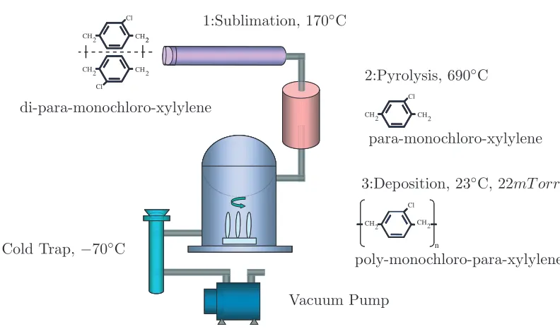
3.1.1 Chemical Structure and Deposition Process . . . 54
3.1.2 Properties . . . 56
3.1.2.1 Mechanical Properties . . . 56
3.1.2.2 Electrical Properties . . . 57
3.1.2.3 Thermal Properties . . . 57
3.1.3 Parylene as a MEMS Material . . . 57
3.2 Parylene Pyrolysis . . . 58
3.2.1 Pyrolysis . . . 58
3.2.2 Process . . . 60
3.2.2.1 Appearance and Thickness Change . . . 60
3.2.2.2 Weight Loss . . . 60
3.2.2.3 TEM . . . 61
3.2.2.4 TGA, DSC, and Raman Analysis . . . 61
3.2.3 Processing of Pyrolyzed Parylene . . . 63
3.2.3.1 Adhesion . . . 66
3.2.3.2 Patterning . . . 66
3.2.4 Mechanical Properties . . . 67
3.2.4.1 Density . . . 67
3.2.4.2 Young’s Modulus and Stress . . . 67
3.2.4.3 Surface Properties . . . 68
3.2.5 Electrical Properties . . . 70
3.2.5.1 Resistivity . . . 70
3.2.5.2 Contact Resistance . . . 71
3.2.5.3 Temperature Sensitivity . . . 74
3.2.5.4 Humidity Sensitivity. . . 75
4 Uncooled Pyrolyzed-Parylene Carbon Bolometer 84
4.1 Design . . . 84
4.2 Fabrication . . . 88
4.2.1 Process Flow . . . 88
4.2.2 Processing Issues . . . 89
4.3 Results. . . 90
4.3.1 Electric Parameters . . . 90
4.3.2 Thermal Properties . . . 91
4.3.2.1 Thermal Conductivity . . . 94
4.3.2.2 Thermal Capacitance and Thermal Capacity . . . 96
4.3.3 Noise . . . 96
4.3.4 Analysis . . . 99
4.4 Conclusion . . . 101
5 Uncooled Carbon Thermal Imager 105 5.1 Design . . . 105
5.1.1 Pixel Layout . . . 105
5.2 Fabrication . . . 106
5.2.1 Dry-Etch Bulk Micromachining Process . . . 106
5.2.2 Wet-Etch Bulk Micromachining Process . . . 109
5.3 Characterization . . . 112
5.3.1 Electrical Properties . . . 112
5.3.2 Thermal Properties . . . 112
5.3.3 Noise . . . 114
5.3.4 Performance . . . 114
5.4 Thermal Imaging . . . 115
5.4.1 Testing Setup . . . 115
5.4.2 Results . . . 120
5.5 Conclusion . . . 121
List of Figures
1.1 Sir William Herschel Discovering Infrared Radiation . . . 2
1.2 Atmosphere Transmission Spectrum . . . 4
1.3 Some Examples of Thermal Imaging Applications . . . 6
1.4 Absorbtion Coefficient for Various Materials, from [7] . . . 7
1.5 Evolution of the Uncooled Infrared Industry in the US, from [20] . . . 11
2.1 Langley’s Bolometer With its Optics . . . 16
2.2 Concept of Radiance . . . 17
2.3 Radiation Exchange Between Two Infinitesimal Surfaces. . . 18
2.4 Spectral Exitance of a Blackbody at 300oK . . . . 19
2.5 Typical Imager . . . 22
2.6 Imaging System Geometry Definitions . . . 23
2.7 Bolometer Principle . . . 26
2.8 Bolometer Equivalent Electric Circuit . . . 27
2.9 Simple Bolometer Readout Circuit . . . 29
2.10 Ideal NETD as a Function of Gleg, adapted from [12] . . . 40
2.11 Spectral Exitance of Blackbody Sources at Different Temperatures . . . 42
2.12 Noise Behavior for Different Integration Times . . . 50
3.1 Chemical structure of different types of parylenes. . . 54
3.2 Parylene Deposition Process . . . 55
3.3 Di-para-xylylene Dimer . . . 55
3.4 Parylene C Film . . . 56
3.5 Thickness Change . . . 61
3.6 Weight Loss. . . 62
3.8 Pyrolyzed Parylene Diffraction Pattern . . . 63
3.9 TGA and DSC, courtesy of [20]. . . 64
3.10 Raman Analysis, courtesy of [20] . . . 64
3.11 Patterned and Selectively Metallized Pyrolyzed Parylene . . . 65
3.12 Pyrolyzed Parylene Free-standing Bridges . . . 65
3.13 Density as a Function of Pyrolysis Temperature . . . 68
3.14 Young’s Modulus and Stress . . . 69
3.15 Contact Angle . . . 69
3.16 Sheet Resistance Test Structure . . . 71
3.17 Pyrolyzed Parylene Resistivity as a Function of Pyrolysis Temperature . . . 72
3.18 Contact Resistance Test Structure . . . 72
3.19 Contact Current-Voltage Characteristic . . . 73
3.20 Contact Resistance as a Function of Pyrolysis Temperature . . . 73
3.21 Temperature Dependence . . . 74
3.22 TCR Dependence on Resistivity . . . 75
3.23 VOx TCR Dependence on Resistivity, after [28]. . . 76
3.24 a-Si TCR Dependence on Resistivity, after [29] . . . 76
3.25 Pyrolyzed Parylene Resistance Change Upon Exposure to Air. . . 77
3.26 Pyrolyzed Parylene Resistance in Air . . . 78
4.1 Typical Bolometer Design . . . 85
4.2 Two-level Pyrolyzed-Parylene Bolometer Design . . . 87
4.3 Fabrication Process Flow . . . 88
4.4 XeF2-Released Fabricated Pyrolyzed-Parylene Bolometers . . . 89
4.5 Bolometer Chip Wire-bonded in PGA Package . . . 90
4.6 Bolometer I-V Characteristic . . . 92
4.7 Bolometer Electrothermal Behavior . . . 92
4.8 Bolometer Electrothermal Behavior at 100T orr . . . 95
4.9 Bolometer Electrothermal Behavior at 100T orr . . . 95
4.10 Bolometer Dynamic Response. . . 97
4.11 1/f Noise Measurement Setup . . . 97
4.13 Noise Power Factor Evolution as a Function of Bias . . . 99
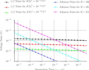
4.14 Noise Contributions for τpulse = 100µs . . . 101
4.15 NETD for Varying Integration Time forVb = 5V . . . 102
5.1 Pixel Layout . . . 106
5.2 Process-Flow for Dry Release . . . 107
5.3 Process-Flow for Wet Release . . . 109
5.4 Pixel Before Release . . . 110
5.5 Release Bolometer Array . . . 111
5.6 Bolometer Pixel Power-Resistance Relationship . . . 113
5.7 Low Noise Power Spectrum . . . 114
5.8 Schematic of Testing Setup . . . 117
5.9 Thermal Imager Chip Seen Through ZnS Window . . . 117
5.10 AMTIR Lens . . . 118
5.11 Thermal Imager Readout Setup . . . 119
5.12 Readout Software . . . 120
5.13 Soldering Iron Tip at 3m . . . 121
List of Tables
1.1 Infrared Wavelength Regions . . . 3
2.1 Emissivity of Various Materials . . . 20
2.2 Parameters of a 240*336 Array of VOx Bolometers, from [14] . . . 44
2.3 Parameters of a 128*128 Array of Titanium Bolometers, from [15] . . . 45
3.1 Selected Mechanical Properties of Parylene [1] . . . 56
3.2 Selected Electrical Properties of Parylene [1] . . . 57
3.3 Selected Thermal Properties of Parylene [1] . . . 58
3.4 Sheet Resistance of 6µm films of Photoresist after Pyrolysis, after [17] . . . . 59
3.5 Comparison of Etching Rates in RIE . . . 67
3.6 Summary of Key Properties of Pyrolyzed Parylene . . . 78
4.1 Pyrolyzed-Parylene Parameters of Interest. . . 91
4.2 Summary of Bolometer Parameters. . . 100
5.1 Bolometer Noise Contributions . . . 115
Notations, Abbreviations and
Physical Constants
Quantity Symbol Unit
Voltage Responsivity ℜ V.W−1
Temperature Coefficient of Resistance TCR α K−1
Radiant Flux Φ W
Spectral Radiant Flux Φλ W.m−1
Radiance L W.m−2
.sr−1
Exitance M W.m−2
Irradiance E W.m−2
Intensity I W.sr−1
Spectral Radiance Lλ W.m−3.sr−1
Spectral Exitance Mλ W.m−3
Spectral Irradiance Eλ W.m−3
Numerical Aperture N A 1
F-number F 1
Noise Voltage Vn V
Johnson Noise Voltage Vj V
1/f Noise Voltage Vf V
Noise-Equivalent Temperature Difference N ET D K
Focal Length f m
Thermal Conductivity Gth W.K−1
Thermal Conductance κ W.K−1
.m−1
Thermal Time Constant τth s
Heat Capacity Cth J.K−1
Specific Heat Capacity C J.Kg−1
K−1
Volumetric Heat Capacity Cv J.m−3
Boltzmann Constant k J.K−1
Temperature T K
Bias Current Ib A
Bias Voltage Vb V
Detectivity D∗
m.Hz1/2W−1
Wavelength λ m
Resistance R Ω
Resistivity ρ Ω.m
Contact Resistance ρc Ω.m2
Conductivity σ Ω−1
.m−1
Activation Energy Ea J
Bandwidth B Hz
Hooge Constant αH 1
Acronym Description
AC Alternating Current
DC Direct Current
IR Infrared
MWIR Medium Wavelength Infrared
LWIR Long Wavelength Infrared
NIR Near Infrared
TCR Temperature Coefficient of Resistance
NETD Noise Equivalent Temperature Difference
NEP Noise Equivalent Power
LPCVD Low Pressure Chemical Vapor Deposition
PECVD Plasma Enhanced Chemical Vapor Deposition
VOx Vanadium Oxide
MCT Mercury-Cadium-Telluride
CMP Chemical-Mechanical Polishing
TEM Transmission Electron Microscope
TGA Thermogravimetric Analysis
DSC Differential Scanning Calorimetry
CMOS Complementary Metal-Oxide Semiconductor
RIE Reactive Ion Etching
DRIE Deep Reactive Ion Etching
TMAH Tetramethyl Ammonium Hydroxide
HMDS Hexamethyldisilazane
AMTIR Amorphous Material Transmitting Infrared
GPIB General Purpose Interface Bus
STI Shallow Trench Isolation
Constant Symbol Value Unit
Boltzmann Constant k 1.38065 10−23
J.K−1 Planck Constant h 6.62607 10−34
J.s−1 Stefan-Boltzmann Constant σb 5.6704 10−8 W.K−4.m−2
Speed of Light in Vacuum c 2.9979 108 m.s−1 Electron Charge q 1.6021 10−19
Chapter 1
Introduction
1.1
Infrared Light and Thermal Imaging
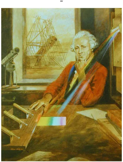
In 1800, German-born British astronomer and Uranus discoverer William Herschel was
studying solar radiation. Using a prism to separate the different wavelengths while
mon-itoring the change in temperature on thermometers in the different color regions (Figure
1.1), he noticed, by design or by chance that if he put a thermometer beyond the red region, the corresponding temperature was increasing as well. He wrote[1]:
“Thermometer No. 1 rose 7 degrees, in 10 minutes, by an exposure to the
full red coloured rays. I drew back the stand,... thermometer No. 1 rose, in 16
minutes, 8 3/8 degrees when its center was 1/2 inch out of the visible rays of the
sun. ...The first four experiments prove, that there are rays coming
from the sun, which are less refrangible than any of those that affect
the sight. They are invested with a high power of heating bodies but
with none of illuminating objects; and this explains the reason why
they have hitherto escaped unnoticed.”
He had just discovered infrared radiation.1
The term “Infrared” from Latin infra, “below,” is usually considered to apply to
wave-length between 700nm and 1mm. It can be argued that the first occurrence of infrared
sensing actually goes back several millennia, when men placed their hand over a recently
extinguished fire [2]. However, until Herschel’s experiment this kind of infrared was simply
1
Figure 1.1: Sir William Herschel Discovering Infrared Radiation
known as heat, or “radiant heat,” and no one wondered what its similarities were with
visible light[1].
In 1879, Joseph Stefan concluded from experimental data that the power transferred
between two bodies was proportional to the difference of the fourth power of their
tempera-ture, a result later theoretically proven by Ludwig Boltzmann in 1884[3]. In 1896, Wilhelm
Wien experimentally found that the wavelength of maximum radiation of a blackbody is
inversely proportional to its absolute temperature[4]:
λmax =
0.28978
T (1.1)
However, Wien’s attempts to find the blackbody radiation distribution law failed. It was
in 1901 that Max Planck first published the correct blackbody radiation law [5], giving
the spectral exitance of the electromagnetic radiation emitted by a blackbody at a given
temperature
Mλ(T, λ) =
2πhc2
λ5(e(hc/λkT)−1)(W.m
−3
Near Infrared NIR 0.7µm−1.4µm Short Wavelength Infrared SWIR 1.4µm−3µm Medium Wavelength Infrared MWIR 3µm−8µm
Long wavelength LWIR 8µm−15µm
Far Infrared FIR 15µm−1000µm
Table 1.1: Infrared Wavelength Regions
whereMλ is the spectral exitance,λthe wavelength considered,h Planck’s constant,cthe
velocity of light in vacuum, and T the temperature (see Section 2.2.1for more details on blackbody radiation).
1.1.1 Types of Infrared Light
What is considered to be infrared light spans 3 orders of magnitude and is usually divided
into several regions that have different practical significance (Table1.1). The near infrared spans from 1.5µmto 1.4µm. It is used in telecommunications and is itself subdivided into
several regions. Another application for near-infrared is remote sensing, e.g., to study and
detect vegetation by their optical signature. Short and medium wavelength infrared can be
used to detect some gases. Long wavelength infrared (8µm−14µm) finds its main use in thermal imaging [6].
1.1.2 Atmospheric Transmission
Figure 1.2 shows the transmission spectrum of the earth’s atmosphere through a 1km path. Due to absorption from water and carbon dioxide, the atmosphere is not transparent
to all infrared wavelengths. As can be seen on the figure, there are two bands of
wave-length to which the atmosphere is transparent: the 3µm−5µmand the 8µm−14µm. The earth’s temperature being around 300K, most of the radiation it emits is around 10µm
in wavelength (see Section 2.2.1.4 for more details). Therefore, the earth’s atmosphere is transparent to the earth’s radiation. Note that if that was not the case, the earth
temper-ature would be much higher and we would not be here to talk about it. The atmosphere of
Venus ,for example, is much “thicker” than that of Earth. For this reason, its temperature
is as high as 450◦
co2
h2o h2o co2 h2o
Figure 1.2: Atmosphere Transmission Spectrum
between the sun and the earth.
1.1.3 Remote Temperature Sensing and Thermal Imaging
For objects close to room temperature (300K), Wien’s displacement law (Equation 1.1) predicts the wavelength of maximum blackbody emission around 10µm. From the
Stefan-Boltzmann law and Planck’s radiation law (Equation1.2), the amount of infrared emitted by a blackbody is a strong function of its temperature. Therefore, to remotely measured
the temperature of an object, one must be able to measure the amount of infrared radiation
it emits, preferably in the 8µm−14µm atmospheric window. It is also possible to use the 3µm−5µmwindow, but less infrared is emitted in this range, making it more demanding on the infrared detector that is used. Thermal imaging, which refers to the ability to measure
the temperature on different points on a scene, requires either an array of infrared detectors
operating in those wavelength ranges or a way to scan a scene using a single detector.
There are many applications to thermal imaging, civilian or military:
• Night vision
• Perimeter surveillance
• Vehicule/personnel detection
• Industrial process monitoring
• Law enforcement
• Driver’s vision enhancement
• Public Health (e.g., detecting individuals with fever in airports)
Figure 1.3 shows some examples of thermal images obtained with commercial uncooled thermal detector arrays.
1.2
Infrared Detectors
The different types of infrared detectors can be put in two categories: photon detectors
and thermal detectors.
1.2.1 Photon Detectors
Photon detectors directly convert incoming photons into photocurrents. The energy of
a photon having wavelengthλis
E = hc λ
E(eV) = 1.24 λ(µm),
where c is the speed of light in vacuum and h is Planck’s constant. To detect infrared
radiation, photon detectors use phenomena that are activated by energies between≃0.1eV (for LWIR) to≃1.8eV (for NIR).
Photodiodes In a photodiode, incoming photons are absorbed and generate
electron-hole pairs that are give rise to a photocurrent. For the photons to be absorbed by the
semiconductor, the bandgap of the semiconductor must be higher than the photons’ energy.
Figure 1.4 shows the absorption coefficient of several detector materials as a function of wavelength. For a given material, the achievable photodiode signal-to-noise ratio depends
on the ratio Gα, whereαis the absorption coefficient andGthe rate of thermal generation of
free charge carriers. In the LWIR range, i.e., the most suitable range for thermal imaging, it
(a) Preventive Maintenance/Process Monitoring (www.indigo.com)
(c) Night Vision on Combat Field (www.indigo.com)
(d) Perimeter Surveillance (www.ulis-ir.com)
Figure 1.4: Absorbtion Coefficient for Various Materials, from [7]
obtain a good performance. One common material for LWIR detection and thermal
imag-ing is Mercury Cadmium Telluride (HgCdT e, also called MCT). Other possible materials
include Indium Antimonide (InSb), Indium Gallium Arsenide (InGaAs), Indium Gallium
Antimonide (InGaSb), Mercury Zinc Telluride (HgZnT e), Mercury Manganese Telluride
(HgM nT e) [7]. The bandgap of these materials can be engineered to correspond to various
wavelength. For example, the bandgap ofHg1−xCdxT e was experimentally found to be[8]
Eg(eV) =−0.302 + 1.93x−0.81x2+ 0.832x3+ 5.35∗10−4
(1−2x)T. (1.3)
Extrinsic Photoconductors: In extrinsic photoconductors, incoming photons excite
electrons in the valence band to impurity levels inside the forbidden band. Therefore, the
energy of interest is not the semiconductor bandgap but the distance between the valence
level Ev and the impurity level. Highly-doped silicon detectors have been demonstrated
using Si:In,Si:As, and Si:Ga. Again, for operation in the LWIR, this energy is small
compared to thermal energy, and the devices require cooling.
Quantum Well Infrared Photodetectors (QWIP): In Quantum Well Infrared
Pho-todetectors (QWIP), multilayer materials are used to create quantum wells. The energy
levels are engineered so that the energy of infrared photons can excite electrons from those
Similar to other photon detectors, QWIP need to be cooled. Even though the performance
of QWIP is not as good as MCT photodiodes, their uniformity and operability and yield
are higher. However, in cooled systems the cooling system accounts for a significant part of
the total cost [7].
1.2.2 Thermal Detectors
Although technically also “photon detectors”, thermal detectors are referred to this
way because they first convert photons into heat before measuring the induced change in
temperature. A thermal detector comprises an absorber which is thermally insulated to
give a big temperature change upon incoming radiation. Several physical mechanisms can
be used to measure this change in temperature. The main types of detection mechanisms
are briefly described below.
Gas Expansion: In 1936, Hammond Hayes published a paper entitled “A receiver of
Ra-diant Energy” in which he reported a new type of thermal detector[9]. He used pyrolyzed
flower pappus as a “fluff,” or gas absorber inside a closed chamber. When absorbing
radi-ation the gas inside the fluff expanded and would cause a chamber wall displacement. The
displacement was then measured capacitively, hence making device operable in Alternating
Current (AC) only. Based on the same idea of gas expansion, Harold Zahl and Marcel Golay
fabricated a “pneumatic infrared detector” published in 1946 [10]. Their device also used
the expansion of a gas due to heat temperature, but the way to detect the gas expansion
was through optical interference instead of an electrical signal. In 1947, Golay published
another paper presenting an improved version using light deflection from a flexible mirror
as a way to detect the gas expansion[11]. In a scanning configuration he demonstrated how
to display the “heat image” of an airplane in flight.2 Even though he was not the first to
use gas expansion as a way to detect infrared light, this type of infrared detector is known
as a “Golay Cell”. They are still commercially available today.
Thermopiles: In 1821, Thomas Seebeck discovered the thermoelectric effect and made
the first thermocouple. Seven years later, Leopoldo Nobili made the first “radiation
thermo-couple” using six antimony-bismuth thermocouples in series [12]. The electromotive force
2
appearing across a thermopile made ofnthermocouples is given by
∆V = n
Z T+∆T
T
Sa(T)−Sb(T)dT
= ∆T n(Sa−Sb) if Sa(T) =Sa and Sb(T) =Sb,
where Sa and Sb are the Seebeck coefficients of the two materials the thermocouples are
made of.
Pyroelectric Detectors: Pyroelectric detectors use pyroelectric materials to measure
the temperature change caused by infrared radiation. Pyroelectric materials are materials
that change polarization upon change in temperature. Pyroelectric detectors can only
operate in AC mode, as free charges will cancel the obtained polarization in DC. The
current flowing into or out of a pyroelectric detector made out of two electrode in between
which is a pyroelectric material, is given by [13]
I =ApdT
dt, (1.4)
where A is the area of the electrodes, p the pyroelectric coefficient, and dTdt the rate of
temperature change.
Thermomechanical Detectors: Thermomechanical infrared detectors use deflection of
composite cantilevers made of two materials having different coefficients of thermal
ex-pansion. This type of composite cantilever is called a bimetalic cantilever or a bimaterial
cantilever. They are (or were used) as low-cost temperature detectors in everyday
applica-tions, such as kitchen ovens or blinking Christmas decorations. The deflection at the tip of
the cantilever is given by [14]
∆z=C∗L3(α1−α2)∆T, (1.5)
whereCis a constant that depends on the materials’ thicknesses and their Young’s modulus,
Lis the length of the cantilever, andα1 andα2 are the coefficients of thermal expansion of
the two layers. There are several ways this deflection can in turn be measured, e.g., optical
sensing.
Bolometers: Bolometers are thermal sensors that use a thermistor to measure the
tem-perature change induced by incident infrared radiation. The change in bolometer resistance
due a change in temperature is given by
∆R=αR∆T, (1.6)
where α is the temperature coefficient of resistance of the thermistor and ∆T the
temper-ature change due to the incident radiation.
The theory and current state of the art of bolometers is described in detail in Chapter
2.
1.3
Micromachining for Uncooled Thermal Imaging
Since thermal detectors rely on a change of temperature induced by radiation, the
sensing element of a thermal sensor must be thermally insulated. Given the dimensions
achievable by conventional machining, this thermal insulation causes thermal detectors to
be much slower than photon detectors. Therefore during most of the twentieth century,
photon detectors were preferred to thermal detectors. However, as microelectronic
fabrica-tion techniques matured dramatically because of their use in integrated circuits, it became
possible to fabricate thermal detectors that were well thermally insulated and small enough
have an acceptable response time although, not comparable to that of photon detectors.
All types of uncooled thermal sensors discussed in the previous section have their
micro-machined version. Tunneling micro-Golay cells [15,16], thermopile arrays [17,18],
thermo-mechanical sensors, and arrays [19,14] have been demonstrated. However, so far only two
technologies have found commercial success in uncooled thermal imagers: microbolometer
arrays and pyroelectric arrays.
In the 1980s the US Army Night Vision Laboratory (now part of the U.S. Army’s Night
Vision and Electronic Sensors Directorate, NVESD) and the Defense Advanced Research
Projects Agency (DARPA) funded microbolometer research at Honeywell International Inc.
[2]. The results of this research were declassified in 1992, revealing unexpectedly high
Figure 1.5: Evolution of the Uncooled Infrared Industry in the US, from [20]
At about the same time, the Army Night Vision Laboratory and DARPA also sponsored
research on barium-strontium-titanate (BST) pyroelectric arrays developed at Texas
In-struments (now Raytheon Company). Texas InIn-struments Inc. also worked on bolometers
using amorphous silicon as the thermistor material. The Honeywell technology has since
Bibliography
[1] W. Herschel, “Experiments on the refrangibility of the invisible rays of the sun,”
Philo-sophical Transactions of the Royal Society of London, vol. 90, pp. 284–293, 1800. Avail-able on
http://www.jstor.org/. 1,2
[2] R. Buser and M. Tompsett, “Historical overview,” in Semiconductor and Semimetals (D. D. Skatrud and P. W. Kruse, eds.), vol. 47, ch. 1, Academic Press, 1997. 1,10
[3] P. Kruse, L. McGlauchlin, and R. McQuistan, Elements of Infrared Technology: Gen-eration, Transmission and Detection. John Wiley & Sons, Inc, 1962. 2
[4] “Aerospace science and technology dictionnary.”
http://www.hq.nasa.gov/office/hqlibrary/aerospacedictionary/. 2
[5] M. Planck, “On the law of distribution of energy in the normal spectrum,” Annalen
der Physik, vol. 4, 1901. 2
[6] “Infrared.” Wikipedia, 2005.
http://en.wikipedia.org/wiki/Infrared. 3
[7] A. Rogalski, “Infrared detectors: Status and trends,”Progress in Quantum Electronics, vol. 27, no. 2, pp. 59–210, 2003. xi,7,8
[8] G. L. Hansen, J. L. Schmit, and T. N. Casselman, “Energy gap versus alloy composition
and temperature inhg1−xcdxte,”Journal of Applied Physics, vol. 53, no. 10, pp. 7099– 7101, 1982.
http://link.aip.org/link/?JAP/53/7099/1. 7
vol. 7, no. 5, pp. 202–204, 1936.
http://link.aip.org/link/?RSI/7/202/1. 8
[10] H. A. Zahl and M. J. E. Golay, “Pneumatic heat detector,” Review of Scientific In-struments, vol. 17, no. 11, pp. 511–515, 1946.
http://link.aip.org/link/?RSI/17/511/1. 8
[11] M. J. E. Golay, “A pneumatic infra-red detector,” Review of Scientific Instruments, vol. 18, no. 5, pp. 357–362, 1947.
http://link.aip.org/link/?RSI/18/357/1. 8
[12] McGraw-Hill Encyclopedia of Science and Technology Online.
http://www.accessscience.com. 8
[13] P. Muralt, “Micromachined infrared detectors based on pyroelectric thin films,”Reports
on Progress in Physics, vol. 64, no. 10, pp. 1339–1388, 2001.
http://stacks.iop.org/0034-4885/64/1339. 9
[14] P. G. Datskos, N. V. Lavrik, and S. Rajic, “Performance of uncooled microcantilever
thermal detectors,” Review of Scientific Instruments, vol. 75, no. 4, pp. 1134–1148,
2004.
http://link.aip.org/link/?RSI/75/1134/1. 9,10
[15] T. W. Kenny, W. J. Kaiser, S. B. Waltman, and J. K. Reynolds, “Novel infrared
de-tector based on a tunneling displacement transducer,”Applied Physics Letters, vol. 59,
no. 15, pp. 1820–1822, 1991.
http://link.aip.org/link/?APL/59/1820/1. 10
[16] T. Kenny, “Uncooled infrared imaging systems,” in Semiconductor and Semimetals (D. D. Skatrud and P. W. Kruse, eds.), vol. 47, ch. 8, Academic Press, 1997. 10
[17] M. Foote, E. Jones, and T. Caillat, “Uncooled thermopile infrared detector linear
arrays with detectivity greater than 109cm.hz1/2w−1
,”IEEE Transactions on Electron
Devices, vol. 45, September 1998. 10
[18] A. Schaufelbhl, N. Schneeberger, U. Mnch, M. Waelti, O. Paul, O. Brand, H. Baltes,
based on micromachined cmos integrated sensor array,” Journal Of Microelectrome-chanical Systems, vol. 10, December 2001. 10
[19] Y. Zhao, M. Mao, R. Horowitz, A. Majumdar, J. Varesi, P. Norton, and J. Kitching,
“Optomechanical uncooled infrared imaging system: Design, microfabrication, and
performance,”Journal Of Microelectromechanical Systems, vol. 11, april 2002. 10
[20] J. Tissot, “Ir detection with uncooled focal plane arrays. state of the art and trends,”
Chapter 2
Uncooled Bolometers for Thermal
Imaging
Introduction
The Merriam-Webster dictionary entry for bolometer states:
Etymology: From the Greekbole, ray andmetron, measure.
:A very sensitive thermometer whose electrical resistance varies with
temper-ature and which is used in the detection and measurement of feeble thermal
radiation and is especially adapted to the study of infrared spectra.
Although technically correct, this definition is incomplete because it does not explain how
the presence of radiation leads to a change in temperature and electrical resistance. A
more complete definition could be as follows: “A device that measures thermal radiation
by converting said radiation into a temperature change and subsequently measuring the
induced change in electrical resistance.”
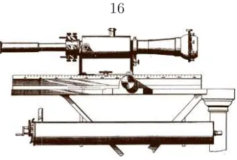
The bolometer was invented in 1878 by Samuel Pierpont Langley while he was studying
radiation of the Sun. Langley’s bolometer consisted of four strips of titanium arranged in
a Wheatsone bridge. Two of the metal strips were painted black and exposed to radiation
while the two others were covered. The signal could be read using a galvanometer. Langley
Figure 2.1: Langley’s Bolometer With its Optics .
2.1
Radiometry
To perform thermal imaging, we need to detect the thermal radiation coming from
an object and we need to know the relationship between the detected radiation and the
object temperature. Radiometry by definition is the science of radiation measurement.
This section introduces several important radiometry definitions. We then lay out the
equations governing the radiation exchange between a blackbody at a given temperature
and a detector through a lens.
2.1.1 Radiant Flux
The radiant flux φ(W) emitted or received by a surface is the power of electromagnetic
radiation it emits or receives.
2.1.2 Irradiance
The irradiance E(W.m−2
) of a surface is the amount of radiant flux it receives per unit
area.
2.1.3 Radiance
The radiance L(W.m−2 .sr−1
) of a surface is defined as the amount of radiant flux it
emits per unit of projected area and per unit of solid angle. This definition is better
understood if placed in the context of radiation exchanges between two surfaces. Let us
consider an infinitesimal element of area of a source dAs having radiance L emitting light
into a light cone dω. Let us call θs the angle between the surface dAs and the direction
dAscosθs
dAs
dω dω
Projected Area θs
d2φ=L(θs)dAscosθsdω
Figure 2.2: Concept of Radiance
projection of this area onto the plane which is normal to the direction of light propagation,
i.e., dAscosθs. Let us now consider the light cone having an elemental solid angle dω
(Figure2.2). Since the definition of radiance is the amount of radiant flux emitted by the source per unit projected area and per unit of solid angle, the radiant flux emitted by dAs
in the light cone subtended bydω is
d2φ=L(θs)dAscosθsdω. (2.1)
2.1.4 Exitance
The exitance M(W.m−2
) of a surface is the total radiant flux it emits per unit area:
M ≡ dΦ dAs
=
Z
L(θs) cosθsdωd. (2.2)
The spectral exitance of a surface is the radiant flux it emits per unit area and per unit
wavelength:
Mλ ≡ dΦλ dAs
=
Z
Lλ(θs) cosθsdωd. (2.3)
where the integrals is taken over an hemisphere.
2.1.5 Intensity
Intensity I(W.sr−1
) is the amount of radiant flux emitted per unit of solid angle:
I = dφ
dω (2.4)
θs
θd r
dAs dA
d dωd
d2φ=L(θs)dAscosθsdωd dωd= dAdrcos2 θd
Figure 2.3: Radiation Exchange Between Two Infinitesimal Surfaces
2.1.6 Radiation Exchange Between Two Surfaces
Let us now consider the radiation exchange between a surfacedAsand a detector surface
dAd, with r the distance between the two surfaces, θs and θd the angle between the light
propagation direction and the surfacedAs and dAd, respectively (Figure2.3).
As seen before from the definition of radiance we have
d2Φ =L(θs)dAscosθsdωd, (2.6)
with dωd the solid angle subtended by dAd from dAs. Using the definitions in Figure 2.3 this can also be written
d2Φ =L(θs)
dAsdAdcosθscosθd
r2 (2.7)
and
d2Φ =L(θs)dAdcosθddωs, (2.8) withdωs the solid angle subtended bydAs from dAd.
2.1.7 Lambertian Surfaces
By definition, the radiance of a Lambertian surface L(θs) is independent ofθs:
L(θs) =L. (2.9)
Let us consider an elemental Lambertian surface dAs located in the center of a receiving
hemisphere of radiusr. By definition, the exitanceM of the surfacedAsis the total amount
of radiant flux emitted per unit of area. In the following the subscript letter, h represents
λ(µm) Mλ(W.cm−1.µm−1)
1∗10−3 2∗10−3 3∗10−3 4∗10−3
5 10 15 20
Figure 2.4: Spectral Exitance of a Blackbody at 300oK
each elemental receiving hemisphere area. From Equation 2.6, we get
M =
Z
Ωh
Lcosθsdωh
=
Z
Sh
LcosθsdSh r2
=
Z π/2
θs=0
Z 2π
ϕ=0
Lsinθscosθsdϕdθs
M = πL. (2.10)
2.2
Thermal Imaging
2.2.1 Blackbody Radiation
2.2.1.1 Definition
A black body is a Lambertian source having spectral exitance given by Planck’s
black-body radiation equation:
Mλ(T, λ) =
2πhc2
λ5(e(hc/λkT)−1)(W.m
−3
). (2.11)
Material Emissivity
Aluminum foil 0.04
Steel (polished) 0.07
Brick 0.93
Glass 0.95
Human skin 0.98
Water 0.96
Wood 0.9
Concrete 0.95
Table 2.1: Emissivity of Various Materials
2.2.1.2 Radiance
From Equation2.10 the spectral radiance is simply
Lλ(T, λ) =
M(T, λ) π (W.m
−3 .sr−1
). (2.12)
Real materials always have an exitance smaller than the ideal blackbody, given by
Lλ(T, λ) =ǫλ
M(T, λ) π (W.m
−3 .sr−1
), (2.13)
whereǫλ <1 is the material spectral emissivity. Materials for which the spectral emissivity
is independent of the wavelength (i.e.,ǫλ =ǫ) are called graybodies. Although these are only
hypothetical since no material emits at all wavelengths of the electromagnetic spectrum,
some materials have spectral emissivities that can be considered constant across wavelengths
of practical interest (e.g., LWIR). Table2.1 shows the emissivities of various materials.
2.2.1.3 Exitance
The total exitance of a blackbody is given by the Stefan-Boltzmann’s law:
M(T) =
Z +∞
0
Mλ(T, λ)dλ=σbT4, (2.14)
2.2.1.4 Wien’s Displacement Law
The wavelength of maximum spectral excitance λmax of a blackbody depends on its
temperatureT. From Equation 2.11,λmax andT can be shown to satisfy the relation
λmaxT =
hc
5k(1−exp− hc
kλmaxT)
, (2.15)
which can be solved numerically to give
λmaxT = 2.8978∗10−3(m.K),
or in a more convenient form
λmax(µm) =
2897.8
T(K). (2.16)
Therefore, objects close to room temperature (T ∼300oK) radiate mostly at wavelengths within the 8µm−14µm atmospheric window (LWIR).
2.2.2 Radiation Transfer Between an Object and a Detector
To remotely measure the temperature of an object or a scene one must collect the
radiation it emits on a detector. In this section, we derive the expression of the irradiance
on a detectorEddue to an object having a spectral exitanceMλ,owhen the radiation coming
from the object is focused on the detector using a lens of focal lengthf and of diameterD.
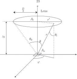
Figure 2.5 shows the typical imaging system configuration. f is the focal distance of the lens ,zo is the distance between the object and the lens, andzi is the distance between the
image (or detector) and the lens.
First we calculate the spectral radiant flux Φλ,o→l being transferred from the object
surfaceAo to the lens surfaceAl. Assuming the there are no losses in the lens, this spectral
radiant flux will then be incident on the detector surfaceAd. Figure2.6shows the geometry definitions used for this calculation.
From Equation 2.1we get
Φλ,o→l(T, λ) =
Z
Ao
Z
Ωl
θi θ0
zi zo
D
2
Lens
Object Image
Figure 2.5: Typical Imager
= AoLλ,o(T, λ)
Z
Ωl
cosθdωl,
wheredωl is the elemental solid angle.
From Figure 2.6, we make the appropriate substitutions
θ = θl,
dωl = dAl
r2 cosθ,
r = zo cosθ, r′
= zotanθ,
dAl = r ′
dϕdr′
= z
2
otanθ
cos2θ dϕdθ,
dωl = sinθdϕdθ,
Φλ o→l(T, λ) = AoLλ,o(T, λ)
Z 2π
0
Z θ0
0
sinθcosθdθdϕ
= AoπLλ,o(T, λ) sin2θ0. (2.17)
For or a Lambertian object we can substitute Equation2.10 into Equation 2.17to get
Φλ,o→l(T, λ) =AoMλ,o(T, λ) sin2θ0. (2.18)
From Abbe’s sine condition (also called the optical sine theorem)[1] we have
Ao
θl
θ θ0
ϕ D
2
r′
r z0
Al
[image:41.612.199.452.55.313.2]Lens
Figure 2.6: Imaging System Geometry Definitions
Therefore, the spectral radiant flux incident on the detector is
Φλ,o→d(T, λ) = AdMλ,o(T, λ) sin2θi = AdMλ,o(T, λ)N A2 Φλ,o→d(T, λ) =
AdMλ,o(T, λ)
4F2 , (2.19)
and the irradiance on the detector surface is
Eλ,d(T, λ) ≡
Φλ,o→d(T, λ) Ad
= Mλ,o(T, λ)
4F2 , (2.20)
where
N A ≡ sinθi (Numerical Aperture) (2.21)
F ≡ 1
2N A = 1 2 sinθi
(F-Number). (2.22)
camera F-number. For an object located at infinity (z0 =f) and if f ≫D, we have
F = 1 D
r
D2
4 +f2
≃ f
D.
In the literature, the focal ratio f /D and F are often considered to be identical and are
simply referred to as “the F-number” or “f/#”. However, this approximation leads to
significant errors whenF is comparable to 1.
2.2.3 Radiation Transfer Between a Blackbody and a Detector
If a blackbody at temperature T radiates to a detector having an area Ad through an
optical system having F-number F, the radiant flux on the detector in the [λ1−λ2] band
is given by integrating Equation 2.19
Φ[λ1,λ2](T) = Z λ2
λ1
Φλ(T, λ)dλ
= Ad 4F2
Z λ2
λ1
M(λ, T)dλ
= Ad 4F2
Z λ2
λ1
2πhc2
λ5(e(hc/λkT)−1)dλ. (2.23)
2.3
Bolometer Theory
2.3.1 Electrical-Thermal Analogy
To study the behavior of thermal systems in general and bolometers in particular, it
is very convenient to use the electro-thermal analogy. To find the thermal equivalent of
electrical quantities, we start by noting that in electronics one studies the behavior and
motion of electrons, i.e., electric charge. In thermal engineering we are interested in the
behavior of thermal energy instead. Therefore, the first step in building the electro-thermal
analogy is stating that electric charge and thermal energy are equivalent:
q(C) ⇔ E(J)
Electric current is the amount of charge that passes through a section per unit of time. The
thermal equivalent is then energy per unit of time, i.e., power:
I = dq
dt(A) ⇔ P = dE
dt (W) Electric Current ⇔ Thermal Power.
The reason why electric charge flows from one region in space to another region in space is
the presence of a potential gradient (electric field). Equivalently, the reason why thermal
energy flows from one region in space to another region in space is the presence of a
temper-ature gradient. Therefore, the thermal equivalent of electrostatic potential is tempertemper-ature:
V(V) ⇔ T(K)
Electric Potential ⇔ Temperature.
Using the same kind of reasoning, one can easily find the thermal equivalents of other
electrical quantities such as current density, conductivity, conductance, and capacitance.
J = dI dS(A.m
−2
) ⇔ Q= dP dS(W.m
−2 )
Current Density ⇔ Thermal Energy Flux,
J =−σ∇V(A.m−2
) ⇔ Q=−κ∇T(W.m−2 )
Electrical Conduction ⇔ Thermal Conduction,
σ(A.V−1 .m−1
) ⇔ κ(W.K−1 .m−1
)
Electrical Conductivity ⇔ Thermal Conductivity,
G= L
σW t ⇔ Gth= L κW t
Electrical Conductance ⇔ Thermal Conductance,
I =CdV
dt ⇔ P =Cth dT
dt
Electrical Capacity ⇔ Thermal Capacity, and
C[C.V−1
] ⇔ Cth[J.K −1
]
Current Bias Ib
Absorber
Incident Radiation Φ
TemperatureT0+GΦth
Heat Capacity Cth Absorptivity η
Thermal ConductanceGleg
Heat Sink (substrate)
Temperature T0
Thermistor
[image:44.612.114.462.69.323.2]ResistanceR(T) TCRα
Figure 2.7: Bolometer Principle
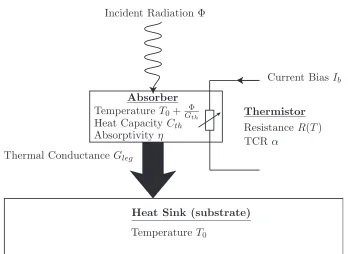
2.3.2 Structure
Figure 2.7shows a simplified bolometer structure. An absorber is linked to a heat sink through a low thermal conductance Gleg. As it absorbs an incident radiant flux Φ(W), the
temperature increases. By measuring the resistance of a thermistor placed on the absorber,
one can calculate the amount of absorbed radiant flux.
2.3.3 Model
Using the electrical-thermal analogy introduced in Section 2.3.1, we can draw the elec-trical equivalent of the bolometer thermal circuit, which is a classical first-order, RC-type
circuit (Figure2.8). The losses through radiation are modeled with a thermal conductance Grad. The expression of Grad is found by taking the derivative of the total exitance of
a blackbody around room temperature (Equation 2.14) and multiplying by the bolometer area 2∗Ad (because both the top surface and the bottom surface of the bolometer are radiating):
Grad = 2Ad dησT4
dT = 8AdσT
T0
ηΦ T
Rleg= 1/Gleg Rrad = 1/Grad
Cth
Universe
Figure 2.8: Bolometer Equivalent Electric Circuit
The total thermal conductanceGth is given by
Gth =Gleg+Grad. (2.25)
The radiation conductance is often neglected, however it should be noted that if the thermal
conductance to the substrateGleg approaches the value of the radiation conductanceGrad,
then both should be taken into account.
2.3.3.1 Static Behavior
In steady state, we have
T(Φ) = T0+
ηΦ Gth ∆T(Φ) ≡ T(Φ)−T0.
Therefore, if the thermistor has a resistance R0 at room temperature and a Temperature
Coefficient of Resistance (TCR) α, we have
R(Φ) = R0(1 +α∆T(Φ))
= R0(1 +α
ηΦ Gth )
∆R(Φ) = R0α
and the voltage signal ∆V measured when biasing the bolometer with a currentIb is1
∆V(Φ) = IbR0α
ηΦ Gth
. (2.26)
Equation2.26 leads to the definition of the voltage responsivityℜ:
ℜ(V.m−1
) ≡ ∆V(Φ)
Φ =
αηR0Ib Gth
. (2.27)
As one would naturally expect from Figure 2.7,ℜ is high when:
1. The absorptivity is high (most of the incoming radiant flux is absorbed and converted
to temperature rise).
2. The thermal conductance is small (good absorber insulation, high temperature rise
for a given absorbed radiant flux).
3. The TCR of the thermistor is big (big change in thermistor resistance for a given
change in absorber temperature).
4. Ib is high (big change in signal voltage for a given change in thermistor resistance).
2.3.3.2 Dynamic Behavior
Let us define
Φ(jω) ≡ Φ0(ω)ejωt (2.28)
and
∆T(jω) ≡ ∆TΦ0(ω)ej(ωt+ϕ). (2.29)
We can write the expression of the thermal transfer function (which, using the electrothermal
analogy of Section2.3.1is equivalent to a complex impedance):
Hth(jω)≡
∆T(jω) ηΦ(jω) =
1
Gth(1 +jωτth). (2.30)
1
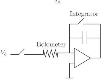
Bolometer
Integrator
[image:47.612.228.397.57.191.2]Vb
Figure 2.9: Simple Bolometer Readout Circuit
It follows that
∆T(ω) = ηΦ0 Gth
p
1 + (ωτth)2 ,
whereτth, the thermal time constant of the bolometer, is given by
τth≡ Cth Gth
. (2.31)
From Equation 2.31, it is obvious that there is a trade-off between D.C. responsivity and thermal time constant. In fact, if one wants to increaseℜ by decreasingGth while keeping τth unchanged, Cth has to be decreased by the same amount as Gth.
2.3.4 Signal Readout
Figure2.3.4shows a simplified bolometer readout circuit in a voltage bias configuration. Typically, a voltage pulse is applied for a duration τpulse, and the resulting current is
integrated. The result of the integration is multiplied by the appropriate coefficient to
give a value of the average bolometer current. The power dissipated by Joulean heating
during readout will cause a temperature increase on the bolometer. Because the thermal
conductivity from bolometer to substrate is low by design, this temperature rise might be
significant. If we assume that the α remains constant during the readout, the temperature
∆T(t) must satisfy
R(∆T)Ib2 = Cth ∆T
dt +Gth∆T,
R0(1 +α∆T)Ib2 = Cth ∆T
and using ∆T(jω) as defined in Equation2.29
∆T(jω) = R0Ib
2
(Gth−R0αIb2) +jCthω = R0Ib
2
Geff+jCthω = R0Ib
2
Geff
1 1 +jωτeff
, (2.32)
with
Geff = Gth−R0αIb2 (2.33)
τeff =
Cth Gef f
= Cth
Gth−R0αIb2
. (2.34)
Equations 2.33 and 2.34 show that the bolometer temperature still exhibits a first-order frequency response. However, depending on the sign of α, the effective thermal constant
can be greater or lower than the intrinsic thermal conductance. The effective time constant
will be lower or greater, respectively. This is due to the fact that for a constant current,
the power injected in the bolometer varies:
∆T(t) =R0Ib
2
Geff
³
1−exp(− t τef f
)´. (2.35)
Equations2.33 and 2.34 show that if α is positive (as would be the case for a metallic thermistor), there exists a critical biasing current Icrit for which Geff and τeff will become
negative:
Icrit=
r
Gth R0α
. (2.36)
IfIb> Icrit, the bolometer will experience thermal runaway, as Equation2.35clearly shows. Such runaway is very likely to destroy or damage the bolometer.2
For t≪τef f we have, from Equation 2.35,
∆T(t) ≃ R0Ib
2
Geff
t τef f
≃ R0Ib
2
Cth
(2.37)
Therefore, ifτpulse ≪τef f, the temperature ∆Tτpulse at the end of the integration pulse of
2
lengthτpulse is
∆Tpulse =
R0Ib2τpulse
Cth
. (2.38)
Equation 2.38 shows that even if α is negative and/or thermal runaway is avoided, the integration timeτpulse and bias currentIb must be chosen so that the temperature increase
∆Tpulse is low enough to avoid damaging the bolometer. Finally, as will be shown in Section
2.3.5,τpulse will affect the bolometer noise performance.
2.3.5 Noise
There are several uncorrelated sources to bolometer noise: the Johnson noise (or thermal
noise), the 1/f noise (also called flicker noise), and the background noise. The 1/f noise
depends on the material used and on the geometry of the device. In this section, we
discuss these different noise contributions in the case of the timed-integration readout circuit
discussed in Section 2.3.4.
2.3.5.1 Readout Circuit Noise Bandwidth
The total noise at the output of a circuit having transfer functionH(f) and input power
noise spectral density Si(f) is given by
< Vn2> =
Z +∞
0
So(f)df
= Si
Z +∞
0 |
H(f)|2df
= SiB, (2.39)
where B is the noise bandwidth defined by
B ≡
Z +∞
0 |
The readout circuit described in Section 2.3.4averages the signal over an integration time
τpulse. Its impulse response h(t) is
h(t) =
0 for t <0
1
τpulse for 0≤t≤τpulse
0 for t > τpulse
and its transfer functionH(f) is
H(f) =e−jπf τpulsesinπf τpulse
πf τpulse
. (2.40)
The noise bandwidth of the readout circuit can be calculated by integrating Equation2.40, but it is easier to calculate it using Parseval’s relation:
B =
Z +∞
0
³sinπf τpulse
πf τpulse
´2
df
= 1
2
Z +∞ −∞
|H(f)|2df
= 1
2
Z +∞ −∞
h(t)2dt
= 1
2
Z τpulse
0
1
τpulse2
dt
B = 1
2τpulse
. (2.41)
2.3.5.2 Johnson Noise
Due to its resistive nature, the bolometer exhibits Johnson (thermal) Noise . J.B.
Johnson experimentally found that the noise power spectral density in a resistor of resistance
R0 given by [2]
Sj = 4kT R0. (2.42)
where k is the boltzmann constant and R0 is the electrical resistance of the bolometer at
room temperature. Equation 2.42was proven theoretically by Harry Nyquist[3].3
When the bolometer signal is read by the integrated and dump circuit presented in
Sec-tion2.3.4, the Johnson noise at the output is found by combining Equation2.42, Equation
3
2.39, and Equation 2.41:
q
< Vj2 >=
s
2kT R0
τpulse
. (2.43)
We conclude this section on Johnson noise by showing that the Johnson noise voltage can
be expressed as a function of the temperature rise the bolometer experiences during the
readout/integration pulse (see Section 2.3.4). Substituting Equation 2.38 into Equation
2.43 gives
q
< Vj2>=Vb
s
2kT
∆TpulseCth
. (2.44)
This important result shows that to minimize the Johnson noise contribution to the total
bolometer noise it is desirable to use materials that can handle a high temperature increase
during readout.
2.3.5.3 1/f Noise
While measuring noise in vacuum tubes, Johnson found that not only was there a white
noise (the thermal noise discussed above) but also another noise component which was
stronger at low frequencies, which he failed to explain [4]. This noise is called 1/f noise, or
flicker noise, and is found in many physical systems, electrical and others[5].
The 1/f noise (or flicker noise) power spectral density of a resistor is given by
Sf(f) = KVb
b
fa (2.45)
whereVbis the bias voltage across the resistor,Kis a constant that depends on the material
used as well as on the geometry of the resistor,ais a constant that depends on the material
and which is usually found to be close to 1, and bis a constant that is usually found to be
between 0.5 and 2 [6]. In many cases, the 1/f noise is equal to (or approximated by)
Sf(f) = KVb2
f . (2.46)
Despite what is believed by some, no resistor is free of 1/f noise. However, the magnitude
In a famous paper published in 1969 [7], F.N. Hooge proposed a “universal” relation
K = αH
nV, (2.47)
wheren is the charge carrier density of the material, V is the total volume of the resistor,
andαH is an empirical constant depending on the resistor material. Some measurements of
αH are collected in [8]. It should be noted that if 1/f noise actually follows Equation2.47, then for a material with fixed sheet resistance (i.e., fixed thickness and fixed resistivity) a
“small” square will have less noise than a “big” square, even though their Johnson noise will
be identical. Such a volume dependence was reported for VOx (vanadium oxide) films and
p-nc-SiC:H films in [9] and [10] respectively. However, little literature is available regarding
1/f noise in materials, and authors often cite values forK in materials without mentioning
the volume of the resistors considered.
We want to calculate the total noise in a pulsed-bias bolometer with integration time
τpulse. In many publications this noise power is calculated using the equation
< Vf2 > =
Z B
f1
Sf(f)df,
leading to a noise power
< Vf2 > = KVb2ln B f1
=KVb2ln 1
2f1τpulse
. (2.48)
where B is the noise bandwidth and f1 is an arbitrary frequency chosen to avoid the
divergence of Sf at f = 0. However, Equation 2.48 is incorrect and is due to a common misunderstanding of the definition of noise bandwidth. It is true that the total thermal
noise is given by
< Vj2 > =
Z B
0
Sj(f)df, (2.49)
but only because Sj(f) = Sj. When a noise power spectral density depends on frequency,
power at the output of the integrating readout circuit is
< Vf2 > =
Z +∞
f1
|H(f)|2KVb
2
f df
=
Z +∞
f1
³sinπf τpulse
πf τpulse
´2KVb2
f df
= KVb2
Z +∞ πf1τpulse
sin2x
x3 dx.
We defineJa,b as
Ja,b =
Z b
a sin2x
x3 dx
=
Z b
a
1−cos 2x 2x3 dx
= hcos 2x−1 4x2
ib a+ 1 2 Z b a
sin 2x x2 dx
= hcos 2x−1 4x2
ib
a−
hsin 2x
2x
ib
a+
Z b
a
cos 2x x dx
= hcos 2x−1 4x2
ib
a−
hsin 2x
2x
ib
a+
Z 2b
2a cosu
u du
= hcos 2x−1 4x2
ib
a−
hsin 2x
2x
ib
a+Ci(2b)−Ci(2a)
= cos 2b−1 4b2 −
cos 2a−1 4a2 −
sin 2b 2b +
sin 2a
2a +Ci(2b)−Ci(2a),
whereCi(x) is the cosine integral defined by
Ci(x)≡ −
Z +∞ x
cosu
u du. (2.50)
then
< Vf2 > = KVb2
Z +∞ πf1τpulse
sin2x
x3 dx
= KVb2Jπf1τpulse,+∞ < Vf2 > = KVb2
³1−cos 2πf1τpulse
4(πf1τpulse)2
+sin 2πf1τpulse
2πf1τpulse −
Ci(2πf1τpulse)
´
. (2.51)
Equation 2.51can be simplified using the fact that in most cases 2πf1τpulse≪1.
The first-order series expansion of Ci(x) is [11]
whereγ = 0.58 is the Euler-Mascheroni constant. Therefore, the first-order series expansion
of < Vf2>is
< Vf2 >=KVb2
³3
2 −γ−ln(2πf1τpulse) +O(2πf1τpulse)
2´
. (2.53)
Equation 2.53shows that Equation2.48 overerestimates the 1/f noise power by
−KVb2( 3
2−γ−lnπ)≃0.22KVb
2.
2.3.5.4 Temperature Fluctuation Noise and Background Noise
An abbreviated and adapted derivation of thermal fluctuation noise and background
noise based on the more general case in [12] is given below. The mean-square fluctuations
in energy of a system with thermal capacity Cth is
<∆E2 > = kT2Cth. (2.54)
This random fluctuation of the energy stored in the bolometer will induce a random
fluc-tuation in bolometer temperature, which in turn will lead to a random flucfluc-tuation of the
bolometer voltage, i.e., atemperature fluctuation voltage noise.
The bolometer temperature and its stored energy are linked through
∆E =Cth∆T (2.55)
From Equation 2.54 and Equation 2.55, the mean-square temperature fluctuation is found to be
<∆TT F2>=
<∆E2 > Cth2
= kT
2
Cth
. (2.56)
Let us assume that this temperature fluctuation is due to a fluctuation in radiant flux ΦT F
and that the power spectral densitySΦT F of ΦT F is independent of frequency. We can write
SΦT F(f) =S0.
Therefore,
<∆TT F2 >=
Z +∞
0
whereHth is the thermal transfer function defined in Equation2.30:
<∆TT F2> = S0η2
Gth2
Z +∞
0
1 1 + (2πf τth)2
df
<∆TT F2> =
S0η2
4GthCth
. (2.57)
Combining Equation 2.56and Equation 2.57, we get
S0=
4kT2G
th
η2 . (2.58)
Using the ∆V =αVb∆T, the power spectral density of the temperature fluctuation voltage
noise can be written
ST F(f) =α2Vb2S0η2|Hth(j2πf)|2 =
4kT2α2Vb2 Gth
1 1 + (2πf τth)2
. (2.59)
However, if the frequencies of interest are much higher than 1/2πτth, the total voltage noise
can be approximated by
q
< VT F2 > = αVb
s
kT2
Cth
(2.60)
(which can also be found using Equation 2.56).
As noted in [12], if most of the heat loss from the bolometer is due to radiation, Gth
reduces to the radiation thermal conductivityGrad = 8ηAdσbT3 and the temperature fluc-tuation noise identifies with the background noise, i.e., the noise due to flucfluc-tuations in the
rate of arrival of photons on the bolometer.
2.3.6 Noise-Equivalent Power
The noise equivalent power (NEP) of a bolometer is defined as the amount of radiant
flux incoming on the bolometer that would lead to a voltage signal equivalent to the noise
power:
N EP ≡ Vn ℜ =
q
V2
j +Vf2+VT F2
2.3.7 Detectivity
The detectivity D∗
, sometimes called “D star”, is a figure of merit that normalizes
performance to the square root of area and bandwidth.
D∗ ≡ ℜ
√ BAd Vn
, (2.62)
where A is the area of the detector and B is the bandwidth of the bolometer/readout
system. The bandwidth of the measurement should also be taken into account because for
any noise power spectral density one could theoretically reduce the total noise by reducing
the bandwidth (e.g., by using an integrator with an arbitrarily long integration time).
However, as noted in [13], detectivity is not a good figure of merit for thermal detectors
(such as bolometers) or thermal imagers. The detectivity was originally defined for photon
detectors. The reason for taking the areaAdinto account in the detectivity is the fact that
in such detectors the dominating noise power (usually generation-recombination noise) is
proportional to the detector area. This is not the case for thermal detectors. In fact, if
one assumes that Hooge’s formula for 1/f noise holds (Equation2.47), the noise power is inversely proportional to the area (for constant thickness).
Some authors use the following alternative definition:
D∗ ′ ≡ ℜ
r
Ad Sn
, (2.63)
where Sn is the total noise power spectral density. If bolometer noise is dominated by
Johnson noise or temperature fluctuation noise, then Vn =√SnB and the two definitions are equivalent. However when 1/f noise is non-negligible, using the alternative definition
overestimates the bolometer performance.
2.3.8 Noise Equivalent Temperature Difference
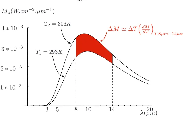
The most relevant figure of merit for bolometers used for thermal imaging is the
Noise-Equivalent Temperature Difference (NETD). It is the smallest temperature change on a
target that one can measure using said bolometer. Quantitatively, the NETD is defined as
the temperature difference on a blackbody target that will lead to a signal-to-noise ratio of
To calculate the NETD of a bolometer, we start by calculating the change in radiant
flux the bolometer will receive when the target temperature changes. The change in radiant
flux falling on the detector peroKchange on the source is found by differentiating Equation
2.23:
dΦλ1−λ2
dT (W.K −1
) =
Z λ2
λ1
dΦλ(T, λ) dT dλ
= Ad 4F2
Z λ2
λ1
M(λ, T) dT dλ
= Ad 4F2
Z λ2
λ1
M(λ, T) hce
(hc/λkT)
kλT2(e(hc/λkT)−1)dλ
= Ad 4F2
³dM
dT
´
T,[λ1,λ2]
,
where
³dM
dT
´
T,[λ1−λ2]
=
Z λ2
λ1
M(λ, T) hce
(hc/λkT
kλT2(e(hc/λkT)−1)dλ. (2.64)
If we d
![Figure 2.10: Ideal NETD as a Function of Gleg, adapted from [12]](https://thumb-us.123doks.com/thumbv2/123dok_us/779976.1090968/58.612.149.439.60.262/figure-ideal-netd-function-gleg-adapted.webp)
![Table 2.3: Parameters of a 128*128 Array of Titanium Bolometers, from [15]](https://thumb-us.123doks.com/thumbv2/123dok_us/779976.1090968/63.612.154.497.231.525/table-parameters-array-titanium-bolometers.webp)