Thesis by Shi (Eric) Luo
In Partial Fulfillment of the Requirements for the degree of
Doctor of Philosophy
CALIFORNIA INSTITUTE OF TECHNOLOGY
Pasadena, California
2018
2017
ACKNOWLEDGEMENTS
The time I spent at Caltech has been has the most memorable learning experience for me on many different levels. I walked onto the campus grounds five years ago, eager to learn, to discover, to grow as a person. Now looking back on this fantastic journey, I’m proud to say I have achieved everything that I have hoped for. Along the way there are so many treasured memories, and so many people to thank.
First and foremost, I would like to thank my thesis advisor, Dr. Julia R Greer, who has been a tremendous resource in the pursuit of my Ph.D. Julia is a constant inspiration for the whole lab, offering us great advises and insightful directions in all our projects, as well as providing constant energy and an uplifting atmosphere around the lab. Julia is also the best advisor in a literary sense that one can hope for. Her care for the students extends way beyond our scientific pursuits, and time and time again she offered me invaluable advice and consoling on many pivotal moments in my Ph.D. career. No matter where my life leads me next, I shall forever remember the door to Julia’s office, covered in heart-warming sketches and drawings, and always open for us to walk in with whatever scientific curiosities or mundane issues that we have.
I would like to express my sincere gratitude to my thesis committee members Drs. William Goddard III, Katherine Faber, and Chiara Daraio, for the time that they dedicated to my thesis and research in general. I’m grateful for the many insightful and fun discussions with them on the different projects that I worked on, and the invaluable advice they each gave me, not just on my thesis research, but how to think and work as a scientist.
manuscript. Dr. Hai Xiao mentored me in various simulation techniques, and also guided me to approach a lot of material science problems from a more fundamental perspective. And last but not the least, Dr. Zachary Aitken has always been a great friend and mentor. His helped me hone my skills in various experimental scenarios, get familiar and truly own the instruments, and brought a sense of positivity and humor to many of our Friday subgroup meetings.
My friends and colleagues are also an integral part to my experience at Caltech. I have yet to see a more tightly bonded, friendly and jovial team than the Greer group, and I’m truly grateful to know all of these fellow scientists. I will treasure the memories of scientific discussions in front of a white board, the Beer Hours every Friday that can have subjects changing from sports to quantum mechanics in a mere minute, and the wild food adventures across the crawling city of Los Angeles. I consider myself really fortunate, to have these colleagues in lab that are also my best friends. Outside the group, I would also like to extend my thanks to the many friends that I met throughout my time at Caltech. This includes fellow APhMS students, my friends from CaltechC, and many more. A lot of us are already scattered across the world, but I’ll look forward to meeting each and every one of you in the next chapter of our lives.
ABSTRACT
Material microstructures is a very broad subject that encompasses most of the field of materials science. Advances in materials characterization and small scale mechanical experiments have brought about progress in the understanding of microstructural features and mechanisms down to the nanometer scale. In contrast to bulk features and properties, the small length scale of these microstructures lead to many interesting properties, and often requires a material-by-material, and even localized region-by-region study. While a thorough understanding of microstructural effects even in one material system is way beyond the scope of this thesis, there are nonetheless many common themes and properties that link together microstructures and their effects on different materials, especially in terms of mechanical properties.
PUBLISHED CONTENT AND CONTRIBUTIONS
Z. Aitken, S. Luo, S.N. Reynolds, C. Thaulow, J.R. Greer, Microstructure provides insights into evolutionary design and resilience of Coscinodiscus sp. frustule, Proc Nat'l
Acad Sciences of the USA 113 (8), 2017-2022 (2016), DOI: 10.1073/pnas.1519790113 Personal contribution: Conducted material characterization (microscopy, spectroscopy) and finite element simulations, helped writing the manuscript.
S. Luo, C. Eisler, T. Wong, H. Xiao, C. Lin, T. Wu, C. Shen, J. Shieh, C. Tsai, C. Liu, H.A. Atwater, W.A. Goddard III, J. Lee, J.R. Greer, Suppression of surface recombination in CuInSe2 (CIS) thin films via Trioctylphosphine Sulfide (TOP:S) surface passivation,
Acta Materialia 106, 171-181 (2016), DOI: 10.1016/j.actamat.2016.01.021
Personal contribution: Designed and conducted material characterization experiments and density functional theory simulations, wrote the manuscript.
S. Luo, J.-H. Lee, C.-W. Liu, J.-M. Shieh, C.-H. Shen, T.-T. Wu, D. Jang, J.R. Greer, Strength, Stiffness, and Microstructure of Cu(InGa)Se2 Thin Films Deposited via
Sputtering and Co-Evaporation, Applied Physics Letters 105 (2) (2014), DOI: 10.1063/1.4890086
TABLE OF CONTENTS
1.2 Effect of Grain Structures on Material Properties 2
1.3 Materials Size Effect: Smaller is Stronger and More 4
1.4 Techniques and Challenges 8
1.4.1 Microstructural Characterization 8
1.4.2 Nano-mechanical Testing 11
1.4 Research Goal and Thesis Layout 13
CHAPTER 2 : CIGS SOLAR CELLS 14
2.1 CIGS solar cells and history 14
2.2 Deposition Methods of CIGS thin films 19
2.2.1 Co-evaporation 20
2.2.2 Sequential Selenization 23
2.2.3 Non-vacuum techniques 24
2.3 Factors that affect CIGS solar cell efficiency 26
2.3.1 Na Diffusion and Incorporation 26
2.3.2 Mo Back Contact 28
CHAPTER 3 : MICROSTRUCTURE AND MECHANICAL PROPERTIES OF CIGS THIN FILMS
FROM DIFFERENT FABRICATION PROCESSES 31
3.1 Introduction 32
3.2 Methods 33
3.3 Results 37
3.3.1 CI(G)S Samples and Device Measurements 37
3.3.2 Morphology and Microstructure 38
3.3.3 Stresses in the Co-evaporated CIGS Films 41
3.3.4 Elastic Properties of the Selenized CIGS Films 43
3.3.5 Mechanical Properties and Deformation of Co-Evaporated Films 46
3.4 Discussion 49
3.4.1 Morphology and Microstructure 49
3.4.2 Thin Film Stress Analysis 51
3.4.3 Pillar Compression 54
3.5 Summary 55
CHAPTER 4 : EFFECTS ON NA DIFFUSION AND SURFACE MICROSTRUCTURE FROM
TOP:S PASSIVATION OF CIGS THIN FILMS 57
4.1 Introduction 58
4.2 Method 60
4.3 Results 64
4.3.1 Surface Measurements of TOP:S Passivated CIS Films 64
4.3.2 Analysis of Through-thickness Na Concentration Profile 69
4.3.4 Calculation of NaCu Energetics at the Film Surface 78
4.4 Discussion 85
4.4.1 Na Distribution in the Presence of TOP:S Passivation 85
4.4.2 Formation Energy of Na in Bulk CIS 91
4.4.3 Effects of Surface Condition on Formation Energy of NaCu 91
4.4.1 Effect of TOP:S on Surface Formation Energy of NaCu 92
4.5 Summary 94
CHAPTER 5 : MICROSTRUCTURE AND HIERARCHY IN HARD BIOMATERIALS 96
5.1 Structural hard bio-materials: an overview 97
5.2 Nacre and Mollusk Shells: Simple but Effective Brick and Mortar Structure 98
5.3 Bone: Complex Microstructure and Hierarchy Lend to Multiscale Toughening Mechanisms 100
5.3 Diatoms: Simple Organism with Intricate Hierarchical Design 103
5.5 Man-Made Hierarchical Materials: Inspired by Nature and Leveraging Size Effect 107
CHAPTER 6 : MICROSTRUCTURES AND MECHANICAL PROPERTIES OF DIATOM
FRUSTULES 111
6.1 Introduction 111
6.2 Methods 114
6.3 Results 121
6.3.1 Frustule Morphology and Microstructure 121
6.3.2 Mechanical Experiments 124
6.4 Discussion 128
6.4.1 Microstructure and Silicification in Diatoms 128
6.4.3 Differentiation of frustules layers in mechanical response 131
6.4.4 Strength vs. Relative Density 132
6.4.5 Stress distribution within frustule layers 136
6.4 Summary 138
CHAPTER 7 : CAPTURING THE GEOMETRY, MICROSTRUCTURE AND MECHANICAL PROPERTIES OF MARINE DIATOM FRUSTULES USING NANOSCALE 3-D SILICA
STRUCTURES 140
7.1 Introduction 140
7.2 Methods 144
7.3 Results 148
7.2.1 Characterization and Morphology 148
7.3.2 Mechanical Experiments 152
7.3.3 Finite Element Simulation 155
7.3.4 Fracture Experiments 156
7.4 Discussion 160
7.4.1 Characterization of POSS Microstructure 160
7.4.2 Mechanical Properties of POSS Structures 161
7.4.3 Fracture Toughness and Crack Arrestment in Diatom and POSS 163
7.5 Summary 166
CHAPTER 8 : CONCLUSION AND OUTLOOK 168
LIST OF ILLUSTRATIONS AND TABLES
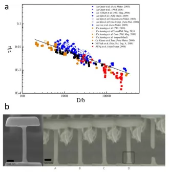
Figure 1.1 Size effect in materials ... 7
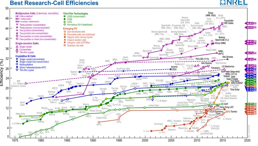
Figure 2.1: Efficiency chart for different photovoltaic materials ... 16
Figure 2.2 Schematic drawing of a typical CIGS solar cell stack ... 18
Figure 2.3 Schematic illustration of different co-evaporation processes ... 22
Figure 3.1 Schematics of common deposition processes for CIGS ... 33
Figure 3.2 Schematics of the CI(G) sample used in this study with thickness measurements of each layer ... 34
Figure 3.3 Measured current-voltage characteristics of selenized and co-evaporated CI(G)S solar cells ... 38
Figure 3.4 SEM and SPM characterization of surface microstructure of selenized and co-evaporated CI(G)S films ... 39
Figure 3.5 TEM and EELS analysis of selenized and co-evaporated CI(G)S films ... 41
Figure 3.6 Nanoindentation results for selenized CIS films ... 45
Figure 3.7 Uniaxial compression experiments of nanopillars from co-evaporated CIGS ... 48
Figure 4.1 XPS and PL measurements on CIS films before and after TOP:S passivation ... 65
Figure 4.2 XPS measurements showing the formation of In2S3 after TOP:S passivation ... 66
Figure 4.4 Na concentration profile in TOP:S passivated and as-fabricated CIS films ... 71
Figure 4.5 Species concentration in as-fabricated CIS films ... 72
Figure 4.6 Species concentration in passivated CIS films ... 73
Figure 4.7 DFT model and results of Na defects in bulk CIS ... 74
Figure 4.8 Total energy for systems with various levels of NaCu substitution... 77
Figure 4.9 Optimized structure of the SP(CH3)3 molecule used in DFT calculations ... 81
Figure 4.10 The effect of Na substitution on optimized geometry of CIS free surface ... 82
Figure 4.11 Formation energy of NaCu at film surfaces with and without TOP:S ... 83
Figure 4.12 Optimized surface geometry with SP(CH3)3 molecule ... 84
Figure 4.13 Ionization potential via low-energy photoelectron spectra of CIS surface ... 88
Figure 5.1The structure, deformation and interfaces of nacre ... 99
Figure 5.2 Microstructures and hierarchy of trabecular bone ... 101
Figure 5.3 Fracture-resisting mechanisms in cortical bones ... 102
Figure 5.4 SEM images of different diatom species ... 104
Figure 5.5 Schematics and SEM images of nanolattices that incorporate hierarchical design ... 109
Figure 6.1 SEM image of a coscinodiscus sp. frustule after the cleaning process ... 115
Figure 6.2 The FIB lift-out process and different samples... 116
Figure 6.3 Schematics and SEM images of coscinodiscus sp. frustules ... 122
Figure 6.5 Mechanical experiments of diatom frustules ... 126
Figure 6.6 Crack propagation and the effect of pores in diatom frustules ... 127
Figure 6.7 Ashby plot of strength versus density for naturally-occurring biological materials ... 134
Figure 6.8 FEA simulation of the von Mises stress in diatom frustule samples during the bending experiments ... 137
Figure 6.9 Stress distribution inside the diatom frustule and the correlation with microstructural features ... 138
Figure 7.1 SEM images the coscinodiscus sp. frustule samples used in this work ... 141
Figure 7.2 Schematics of the sample fabrication process and SEM images of the as-written and baked POSS samples ... 149
Figure 7.3 Characterization of the POSS microstructure, before and after baking ... 151
Figure 7.4 Beam bending and nanoindentation experiments on baked POSS samples ... 153
Figure 7.5 FEA simulation of the bending experiments ... 156
Figure 7.6 Fracture properties of baked POSS and natural diatom frustules ... 158
Table 3.1 Electrical measurements of selenized and co-evaporated samples... 37
Chapter 1
: Introduction
1.1
Microstructure in Materials
The science of materials is, to a large extent, defined in terms of different length scales and their interactions. These length scales can range from single atoms like point defects to ordered arrangement of atoms like grain boundaries and twin boundaries, to macroscopic features visible to the naked eye, like heterogeneous p-n junction in semiconductors. While different length scales would lend different properties to different material systems, it is often the focus on intermediate scales between atomic and macroscopic range that distinguishes a lot of the works in materials science from other fields like physics or chemistry on one end, and mechanical engineering and on the other. Although the exact range is often not properly defined, for the sake of this thesis, the term microstructure refers features in the range of 10 nanometers to 100 micrometers. Examples of features at these length scales include grain boundaries, surface morphology, hierarchy and deformation mechanisms such as dislocation and twinning.1
factor that governs the mechanical properties of materials.6,7 In metals, presence of grain boundaries and twin boundaries often lead to slip planes in a dislocation event5; in ceramics, grain boundaries are also crucial in fracture and lead to catastrophic failure of materials.5
The link between microstructure and their length scale has been of particular interest in the field of mechanics. A full body of literature has been dedicated to discovering the different effect of characteristic length scales in different material systems like fcc, bcc and hcp metal, metallic glass and engineering ceramics.5,8,9 These so called “material size effects” are closely related to the intrinsic microstructure of the material, and the characteristic length scale that’s present in the samples, and has been widely studied and accepted since their discovery. More recently, significant efforts have been devoted to using hierarchical design to introduce a mixture of small and large length scale features to otherwise monolithic material systems, to take advantage of the size effect and reach new materials properties space.1,10–12 An extension of this approach leads to the concept of meta-materials, the careful architecture and hierarchy is used to create materials with completely new properties like negative refractive index.13,14
1.2 Effect of Grain Structures on Material Properties
throughout the whole material, with no grain boundaries. Common examples of single crystalline materials include high purity silicon and diamond. In contrast, polycrystalline consists of many microstructural units of varying shapes, sizes and crystallographic orientations. These ordered microstructures are referred to as “grains”, and properties related to them such as grain size and grain boundaries are often important in material properties.6 Most metals and a lot of ceramics fall under polycrystalline, and their grain sizes can vary from hundreds of nanometers to several milimeters.15 Amorphous materials have no ordered grain structures at any length scale, nor do they have any ordered packing of atoms like single crystalline materials. Instead, amorphous materials often exhibit the same microstructure regardless of the magnification or length scale. The most common amorphous material is probably silica (glass) and metallic glass, which are a special type of metal alloy with no packing order.16
Grain structure is a generalized term that includes features such as grain size, grain boundaries, surface morphology and potential ordered arrangements of grains.17,18 These features, or the lack of them are generally talked about in the context of polycrystalline and amorphous materials respectively.
and even direction of the effects can change based on different materials, like fcc and bcc metals and metallic glasses.19–22 Another example is grain boundary effects in semiconductors. In silicon, grain boundaries serve as recombination sites for carriers leading to increased defect density of states23, and often need to be passivated in high-efficiency devices24; in gallium nitride (GaN) and gallium arsenide (GaAs), grain boundaries decrease carrier mobility25,26, create high defect concentration27,28, and often lead to significantly decreased efficiency compared to single crystalline counterparts29; in chalcopyrite systems such as Cu-In-Se and Cu-Zn-Te, grain boundaries have a more complex effect, with conflicting reports on either increased30 or decreased31,32 efficiency with increasing grain size. These examples serve to show that there is no generalized theory that governs the effect of grain structures in materials. To the contrary these properties should be studied in a careful, case-by-case manner.
1.3 Materials Size Effect: Smaller is Stronger and More
Figure 1.1 Size effect in materials. (a) Shear flow stress
normalized by shear modulus on appropriate slip system for
most face-centered cubic (fcc) metallic micro- and
nano-pillars tested in compression and tension to date. Adapted
from Greer et al.5; (b) SEM image of a typical as-fabricated
100-nm-diameter tensile sample, captured from a movie
recorded during an in situ tension test. The square indicates
necking that was observed before onset of failure. Adapted
1.4 Techniques and Challenges
1.4.1 Microstructural Characterization
Characterizing and visualizing the microstructures are often among the first steps in understanding their effects. Various spectroscopy and microscopy techniques are used to characterize nanometer-to-micrometer scale features. In particular, surface techniques such as scanning electron microscopy (SEM), x-ray photoelectron spectroscopy (XPS), energy dispersive electron spectroscopy (EDS), and cross-section techniques such as transmission electron spectroscopy (TEM) and electron energy loss spectroscopy (EELS) are all frequently utilized in the field.
radiation-implantation effect from FIBs suggests that using a low enough energy, the radiation effect can be contained to be within ~10 nm of the sample thickness73, or almost completely eliminated in some materials systems74. Mechanical studies on FIB-milled micro pillars compared to electro-plated pillars of the same geometry show minimal difference in terms of strength and stiffness75,76. Building upon all these findings, using FIB milling to make site-specific TEM samples is now more popular than ever, and enabled many novel studies especially in the field of small scale mechanics and fracture, where site-specific TEM samples enabled viewing of the sample microstructures after mechanical experiments20,77.
of EDS and EELS results is highly sensitive to background noise and impurities present inside the sample chamber, such as the sample holder or chamber contamination. Thus for proper quantitative analysis, it is imperative to conduct the experiment on a “standard” first: a sample with a known composition that contains the same element as the actual sample.78 On the other hand, qualitative studies such as elemental distribution maps, do not require such standard samples, and are seeing increasingly widespread use in both academic and industrial settings.
1.4.2 Nano-mechanical Testing
FIB-milled micropillars of different materials, inside an SEM that has been custom fitted with a nanoindentor arm90. These experiments combine real time video observation of the sample region of interest (ROI) with precise measurements of the mechanical response, and provide insights into microstructural effects on mechanical properties in various materials systems such as metals21,91, metallic glasses49, ceramics92, and other materials like carbon nanotubes93.
1.4 Research Plan and Thesis Layout
In this work we investigate vastly different materials systems, and investigate how microstructures and hierarchy affects their mechanical, electrical and chemical properties. In doing so we provide results that add to the knowledge base of these materials systems, but more importantly methods and knowledge that can be generalized in the further exploration of “designing” and “engineering” materials.
Chapter 2
: CIGS Solar Cells
We focus our first study of microstructural effects on Copper indium/gallium selenide (Cu(In,Ga)Se2 or CIGS) thin films. CIGS is a mixture of CuInSe2 (CIS) and CuGaSe2 (CGS), which are both p-type polycrystalline semiconductor material belonging to the I–III–VI2 family that have a tetragonal chalcopyrite crystal structure98. CIS and CGS have almost identical crystal structures and properties, since In and Ga are in the same family. For this reason, CIGS also share most of these structure and properties since it’s an ordered mixture of CIS and CGS. Aside from instances where we specifically discuss their differences, CIS/CGS/CIGS will be referred to interchangeably in the following chapters. We will briefly discuss the history, research and current landscape of CIGS in this chapter; in Chapter 3 we will look into how different deposition processes lead to drastically different CIGS film microstructure, and how this affect the film property; in Chapter 4 we will investigate a surface passivation process that seemingly improve CIGS efficiency without changing the microstructure, and show that it achieves this by slight alteration of key defect specie concentration in the film through enhanced solid-state diffusion.
2.1 CIGS solar cells and history
Figure 2.1: Efficiency chart for different photovoltaic materials,
adapted from NREL105
There are several reasons why CIGS is able to reach such high efficiency among thin film photovoltaic materials:
it a prime candidate for low-weight thin film PV applications such as outer-space and portable devices107.
(2) Tunable bandgap: CIS has an intrinsic bandgap of 1.04 eV99. This bandgap increases with increasing Ga concentration as the CIS/CGS alloy mixture shifts towards CGS. With 100% Ga replacement, the bandgap becomes 1.7 eV108. This enables ‘tuning’ of CIGS bandgap by varying In/Ga ratio, and makes CIGS a potential direct bandgap material (a direct bandgap material goes through a one-step excitation-absorption process under incident light) for a wide range of wavelength, as the bandgap can be tuned to accommodate most of the solar spectrum within 1 mm107. This tunable bandgap also results in a tunable, and potentially higher open circuit voltage (Voc), as Voc is directly proportional to the bandgap.
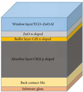
Current commercial and laboratory CIGS solar cells usually adopt a multi-stack layout, as shown in Figure 2.2. Key components of the stack include (from the top): Transparent conducting oxide (TCO) / zinc oxide (ZnO) window layer to allow light to shine through; CdS n-type buffer, CIGS p-type absorber, molybdenum (Mo) back contact and substrate. A p-n junction is created between CdS and CIGS where carriers are collected to generate current. The sputtered Mo back contact is crucial as it can reflect electrons in the CIGS layer back to the p-n junction111. Soda lime glass (SLG) is a common choice of substrate in CIGS devices, and serves the dual purpose of (1) providing a light-permitting, mechanically rigid backbone for the solar cell panel and (2) being the source for Na diffusion into CIGS layer to enhance various electrical properties112.
While CIGS has shown great promise for thin film photovoltaic applications, some limitations and challenges remain for its commercialization. (1) While the requirement on crystallinity during growth process is relatively low, maintaining compositional uniformity between different regions and among different batches is crucial in CIGS fabrication98, as a horizontal compositional gradient or mismatch has been shown to significantly affect device performances113,114. As a result, complex control scheme is required in all CIGS deposition processes, leading to increased equipment and maintenance cost. (2) The fabrication process for CIGS is potentially scalable and more economically viable options compared to some alternative materials. However, the raw materials for CIGS is relatively expensive, especially In and Se, which are supply-limited, which casts an uncertainty on the prospect of the commercialization for CIGS. Given these two limitations, although as a material CIGS is showing great promise in efficiency and application, the current production volume is still small compared to the more mature Si-based solar cells107.
2.2 Deposition Methods of CIGS thin films
been seeing high popularity in recent years: co-evaporation of Cu, In/Ga and Se elemental sources, and sputtering/evaporation of Cu, In/Ga followed by vapor selenization.
2.2.1 Co-evaporation
Figure 2.3 Schematic illustration of different co-evaporation
processes. (a) single stage process, (b) bilayer or Boeing process
(c) three stage process and (d) In, Ga and Cu fluxes are varied
during the growth to obtain a graded structure. In processes (a)–(d),
Using the three-stage method, commercial CIGS solar cells with efficiency 19.3% has been produced122. However, the yield from these co-evaporation processes is limited by the size of the evaporation chamber, which in turn is not yet suitable for commercial up-scaling. As a result, mass production using the co-evaporation process is still being developed.
2.2.2 Sequential Selenization
evaporating a solid Se source98, which significantly increases the manufacturing cost. As a result, H2Se vapor is more commonly used in industrial manufacturing of CIGS.
One downside of the two-step process is lower device efficiency compared to the co-evaporation process. Among the highest-efficiency CIGS cell reported from a two-step process, H2Se process led to an efficiency of 16.2%31, and Se vapor has an efficiency of 19.2%134 both of which are lower than state-of-the-art co-evaporation process at 22%114
2.2.3 Non-vacuum techniques
Electro-chemical deposition processes involve depositing Cu/In/Ga elements in a single-137 or multiple- step138,139 electro-chemical process, while using complexing agents to bring the deposition potentials close to each other. Optimization for these processes is relatively difficult and several studies reported sub-par compositional uniformity after the annealing
step138,140. Highest efficiency values for the electrochemical processes are 13.8% on glass141
and 15.4% on stainless steel142.
Particulate techniques include using screen printing143, spray coating144, or spin coating145 to apply metal precursors in particle form, followed by a high-temperature annealing/sintering step similar to that in other multi-step processes. These methods have the highest efficiency among non-vacuum methods, with recent work using particle mixture of metal oxides and selenide powders achieving 17.1% efficiency on a flexible foil substrate146. However, sintering In/Ga metal particles require high temperature and specialized equipment, which in turn lead to significant cost increase for commercial production. The particle properties also factor heavily into the performance of the final product145.
2.3 Factors that affect CIGS solar cell efficiency
Due to various promising features of the CIGS material, there has been sustained interest in investigating and optimizing the factors that affect CIGS device efficiency. The majority of such research and breakthrough are focused on improving the stack117,149 and fine tuning the deposition parameters31,150. More recently, there has been increasing interest in understanding the microstructure and process in CIGS absorber layer131,151,152. The most notable breakthrough and advances in understanding these effects are summarized in this section.
2.3.1 Na Diffusion and Incorporation
In addition to improving electrical performance of CIGS devices, Na has also been shown to affect grain growth during CIGS deposition. Several reports have suggested that Na enhances formation of grains with (112) orientation, as well as introducing (112) faceted textures on normal (110) grains 153,154. There have also been various reports about Na affecting grain size in CIGS. Some authors suggested an increase in grain size in CIGS films with Na concentration ranging from 0.1% to 0.5%154,163,164, some reported very similar grain size observations in CIGS grown with and without Na112,165,166, and still some reported decreasing grain size with Na introduced via different methods112,150,167. Such differences in literature reports may be due to that Na incorporation and its effect on CIGS grain structure is highly dependent on the deposition processes and conditions, and at the same time these processes and conditions have their own unique effect on the grain structure of deposited CIGS films168.
In summary, although the detailed mechanisms and effects are still unclear, it is widely accepted that Na incorporation plays an important role in both CIGS grain growth and microstructure formation, as well as impacting electrical performance of CIGS solar cell devices. A low Na concentration (< 0.5%) is usually desired, and Na has been shown to congregate to grain boundary and film surfaces157.
the CIGS film169. On other substrates such as polymer or metals, a thin (~ 10 nm) layer of sodium fluoride (NaF) is often deposited before the CIGS layer as a Na source, and the diffusion would activate in a similar thermal process170.
2.3.2 Mo Back Contact
Several metals like platinum (Pt), gold (Au), silver (Ag) and molybdenum (Mo) have all been investigated as electrical back contact for CIS-based solar cells171–173. Mo eventually became the popular choice due to its stability at high temperature, resistance to alloying with Cu and In, and low contact resistance173. Mo back contact on CIGS is usually deposited via evaporation174 or sputtering175,176 on SLG substrate. Several reports have discussed the effect of residual stress174,175, adhesion173,177, and directionality31 of Mo layer. In particular, Mo layer with residual compressive stress has been shown to possess more uniform grain structure and ultimately lead to better electrical performance, whereas Mo layers with residual tensile stress have been reported to have a more porous structure174,175,178.
proposed that MoSe2 layer is mechanically stable with good adhesion and does not significantly impact the electrical performance of the CIGS devices185,186.
The thickness and crystallinity of Mo layer is also important to the operation and performance of CIGS solar cells. For CIGS films deposited on a SLG substrate, Na would diffuse into the absorber layer through the Mo contact. As a result, increased Mo layer thickness would impede the Na diffusion process and lead to negatively affect electrical performance187. Yet a Mo layer that’s too thin would lead to adhesion issues, as well as a decreased fill factor187,188. A well-accepted thickness for Mo layer in CIGS solar cells is between 200 to 400 nm187,189,190.
2.4 Summary
CIGS-based materials are popular candidates for thin film photovoltaic applications mainly due to their high absorption coefficient and unique tunable bandgap. Remarkable progress has been made in this field over the last few decades. Currently CIGS have among the highest efficiency rating in thin film solar cell materials. The ever-increasing amount of research and industrial efforts into CIGS and related devices also show tremendous potential for further enhancement.
Chapter 3
: Microstructure and Mechanical
Properties of CIGS Thin Films from Different
Fabrication Processes
The effect of different deposition methods on film quality and device performance is an important area in the field of CIGS. However, as discussed in Chapter 2, most of the research in this space focus on fine-tuning the deposition recipes and trying to find a direct link between deposition process and device performance. In this chapter which is adapted from Luo et al.191, we use a more fundamental approach to investigate the microstructure and mechanical properties of CIGS thin films fabricated by (1) selenization of pre-sputtered Cu-In-Ga mixture and (2) co-evaporation of each constituent.
nanoindentation data and reveal the indentation modulus of 68.9±12.4 GPa, which is in agreement with previous reports. Uniaxial compression experiments are performed on FIB-milled nanopillars with diameters of ~500nm extracted from co-evaporated films and revealed the elastic modulus of 70.4±6.5 GPa. This equivalence of the elastic moduli suggests that the microstructural differences manifest themselves after the yield point. Typical plastic behavior with two distinct failure modes is observed in the extracted stress-strain results, with the respective yield strength of 640.9±13.7 and 1100.8±77.8 MPa.
3.1 Introduction
Cu(In,Ga)Se2 (CIGS) has become one of the most promising materials for thin film photovoltaics, with recent achievement in efficiency of over 20% on soda lime glass (SLG) substrates122 as compared with traditional polycrystalline silicon cells.192 The thin film nature of CIGS makes it a suitable material for depositing onto lightweight flexible substrates like polyimide (PI) films and metal foils, amenable to roll-to-roll processing, with efficiencies of 18.7% reported for CIGS on PI films193 and of 17.9% on titanium foils194. Current studies of CIGS solar cells have been mainly focused on improving the fabrication process and on fine-tuning cell parameters to achieve better device performance119
in performance between Cu-In-Ga-Se devices fabricated by two different processes: (1) co-evaporation of each individual constituent and (2) selenization of the pre-sputtered Cu-In-Ga mixture. The latter has superior economic potential but its performance has been reported to be ~3/4 of that for the co-evaporated cells, as shown in Figure 3.1.
Figure 3.1 Schematics of common deposition processes for CIGS:
(a) sequential selenization, (b) co-evaporation
This chapter presents microstructural and mechanical characterization of the 1.5 μm -thick CIGS films deposited by co-evaporation and selenization techniques with the goal of developing a better fundamental understanding of the CIGS material and to gain insight into the effects of material processing on device performance.
3.2 Methods
selenization and the other co-evaporation processes. In both processes CI(G)S was deposited on top of a 700 nm molybdenum back contact layer sputtered on SLG substrate in a two-steps process. During the first step, a 70 nm-thick Mo layer was sputtered at a pressure of 10 mTorr; with additional 630nm sputter-deposited during the second step at 3.6 mTorr. Cu and In metal precursors were sputtered onto the Mo contact at 2.8 mTorr and 150 °C, followed by selenization with Se vapor with N2/H2 carrier gas at 550 °C. The total thickness of the CIGS absorber layer was measured via SEM to be 1.6 ± 0.2 μm. For the co-evaporated CIGS, the absorber layer was deposited onto 0.46 cm2 Mo coated SLG substrates using a 3-step homogeneous thermal evaporation of elemental Cu, In, Ga and Se at 550 °C. The overall thickness of the co-evaporated absorber layer was 1.7 ± 0.1 μm. A schematic of the sample stack is shown in Figure 3.2.
Figure 3.2 Schematics of the CI(G) sample used in this study with
thickness measurements of each layer. (a) full cell, (b) films on
substrates. In both cases two different absorber materials are tested:
Imaging and characterization: SEM images were taken using FEI Nova Nanolab 200 FIB/SEM, and EDS within the same instrument was used to ascertain the chemical composition of the sample. Samples were cut into 1 cm × 1 cm pieces for SEM imaging. All SEM images were acquired at a tilt angle of 52 °. Grain sizes were estimated based on the SEM and TEM images in the following manor: (1) multiple lines of the same length were drawn across the image in both horizontal and vertical directions emanating from different, randomly chosen points; (2) number of intersections of the lines with the grain boundaries were recorded; (3) the average grain size is taken to be the total length of the lines divided by the total number of intersections. A micromanipulator (Omniprobe) within the FIB (FEI, Nova200) was used to create nano-pillars for uniaxial micro-compression experiments and to extract site-specific locales within the films. Bright-field images and EELS maps were generated from both samples using Tecnai TF-30 TEM (FEI). The curvature induced in the substrate after the deposition of films was measured using KLA Tencor Laser Interferometer for the neat SLG substrates, SLG/Mo and SLG/Mo/CIGS samples.
3.3 Results
3.3.1 CI(G)S Samples and Device Measurements
While the selenized samples in this work did not contain gallium, it is reasonable to assume that the mechanical and structural properties of CIS should be similar to those of CIGS because of the similarities in the crystal structure and in the atomic sizes of CuInSe2(CIS) and CuGaSe2 (CIGS)198. The chemical composition of each sample is provided in Table 3.1. The current density-voltage (J-V) characteristics were measured on functional cells made from CIS and CIGS films deposited using both methods, as shown in Figure 3.3.
Table 3.1 Electrical measurements of the samples used in this
Figure 3.3 Measured current-voltage characteristics of selenized
and co-evaporated CI(G)S solar cells. c-CIGS: co-evaporated
CIGS films; s-CIGS: selenized CIGS films; s-CIS: selenized CIS
films
3.3.2 Morphology and Microstructure
recorded at 173.5 ± 17.1 nm for the selenized film, a value almost an order of magnitude rougher than the 33.5 ± 4.3 nm in the co-evaporated film. Grain sizes were measured to be similar, 114.6 ± 23.1 nm for selenized films and 147.7 ± 84.9 nm for co-evaporated films based on the SEM images. The large variation in the grain sizes of the co-evaporated films stems from the grains being slender and anisotropic, in contrast to the selenized films, which appear faceted and isotropic. Electron Back Scatter Diffraction (EBSD) analysis was attempted to better quantify the orientation and sizes of the grains but the substantial surface roughness rendered EBSD patterns impractical.
Figure 3.4 SEM and SPM characterization of surface
Representative SEM images of (a) selenized CIS and (b)
co-evaporated CIGS films taken top down with the zoomed-in view of
the center location shown in the inset in the top right corner; and
cross-section views of (c) selenized CIS and (d) co-evaporated
CIGS films taken at 52o. SPM images in (e) and (f) correspond to
the same films. For the RMS roughness values, measurements over
10 different regions on the same film were used for each type of
films
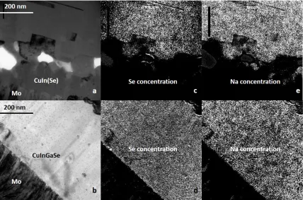
Figure 3.5 TEM and EELS analysis of selenized and co-evaporated
CI(G)S films. Bright field TEM image of (a) selenized and (b)
evaporated films; Se concentration of (c) selenized and (d)
evaporated films; and Na concentration of (e) selenized and (f)
co-evaporated films. Note that in (a) the CuIn(Se) region does not
contain Se, hence the different notation.
3.3.3 Stresses in the Co-evaporated CIGS Films
estimates the residual stress in the film from the measured curvature through Stoney’s
The average bending radii of the substrate were measured on 3 sets of samples: (1) the as-fabricated SLG substrates which had the dimensions of 2cm × 2cm × 2mm, (2) SLG substrates produced from the same batch as in Equation. 1 with 700 nm thick Mo films deposited via a two-step sputtering process, first at 150 °C, and second – at 550 °C, and (3) the same SLG substrates with the 700 nm thick Mo and 1.5 μm-thick CIGS film evaporated on top of the stack at 550 °C. The stress state in the films is likely more complex than biaxial so this approach is used as an estimate, which has been shown to be robust for many material systems in thin film on a substrate form200. Thin film deposition parameters, as well as the measured radii of curvature of the substrate and the calculated biaxial thin film stresses in each film, calculated by Equation 3.1, are shown in Table 3.2. The high stress predicted by Stoney’s relation after the CIGS deposition step is consistent with the bending of the Mo layer observed in SEM and TEM images. (Figures 3.4 and 3.5)
Table 3.2 Sample deposition conditions, measured radius of
curvature and residual stress calculated using Stoney’s relation
Glass
substrate 1× 10⁶ N/A
228
N/A
Molybdenum 800 <150 237.3 14.7 (tensile) CIS
3.3.4 Elastic Properties of the Selenized CIGS Films
The substantial surface roughness of the selenized films prevented conducting similar curvature measurements on these samples. To determine the Young’s modulus and stiffness of the selenized films we used nanoindentation and analyzed the elastic loading data via Hertzian contact model,201 with the deforming grain and the tip of the indenter approximated as elastically-contacting spheres. Indentation was conducted in a Hysitron TI-950 Triboindenter with a Berkovich tip that has an effective radius of curvature R1 of 150 nm;202
the radius of the contacting grains R2 was measured in the SEM to be 500 ± 42 nm by methods
1
Figure 3.6 Nanoindentation results for selenized CIS films.
Displacement (d, y-axis) and load (F, x-axis) data from indentation
of selenized film overlaid with curve-fitting results from Hertzian
contact theory. For each data set, up to 1% of total displacement
was considered to be in the linear regime and showed in the graph.
The smeared curves are the actual data while the thincurves are the
polynomial fit according to Equation 3. The standard Berkovich tip
used and the individual grains on the film were approximated as
spheres. R square values of above 9.87 were reached for all data
3.3.5 Mechanical Properties and Deformation of Co-Evaporated Films
The analysis of compressive response of the CIGS nanopillars was conducted following the methodology of Greer et al..196 We assumed perfectly cylindrical pillars and uniaxial compression to estimate global stresses and strains from the load-displacement data. Conservation of volume during plastic deformation allows us to calculate the instantaneous compression area Apand pillar length Lp and initial pillar height L0 and area A0, with the latter
being an average of top and bottom area of an individual pillar. The total measured displacement, dtot, can be expressed in terms of the elastic component del and plastic
component dp, while del can be expressed in terms of measured stiffness 𝑘𝑘𝑚𝑚𝑚𝑚𝑚𝑚𝑚𝑚𝑚𝑚𝑚𝑚𝑚𝑚𝑚𝑚 and load
on pillar F, which were continuously recorded by CSM; dp would then give us instantaneous
pillar length Lp, and the stress σ.
𝐴𝐴0𝐿𝐿0 = 𝐴𝐴𝑝𝑝𝐿𝐿𝑝𝑝 (3.4)
𝐿𝐿𝑝𝑝 =𝐿𝐿0 − 𝑑𝑑𝑝𝑝 = 𝐿𝐿0 −(𝑑𝑑𝑡𝑡𝑡𝑡𝑡𝑡− 𝑑𝑑𝑚𝑚𝑒𝑒) =𝐿𝐿0− �𝑑𝑑𝑡𝑡𝑡𝑡𝑡𝑡−𝑘𝑘 𝐹𝐹
𝑚𝑚𝑚𝑚𝑚𝑚𝑠𝑠𝑚𝑚𝑟𝑟𝑚𝑚𝑚𝑚� (3.5)
σ= 𝐴𝐴𝑃𝑃 𝑝𝑝 =
𝑃𝑃𝐿𝐿𝑝𝑝
𝐴𝐴0𝐿𝐿0 (3.6)
The true strain ε consists of the elastic part ε𝑚𝑚𝑒𝑒, given by Hooke’s Law, and plastic part ε𝑝𝑝, related to Lp:196
Where 𝐸𝐸𝐶𝐶𝐶𝐶𝐶𝐶𝐶𝐶 is Young’s Modulus for CIGS, obtained from the stiffness 𝑘𝑘𝐶𝐶𝐶𝐶𝐶𝐶𝐶𝐶:197
𝐸𝐸𝐶𝐶𝐶𝐶𝐶𝐶𝐶𝐶 = 𝑘𝑘𝐶𝐶𝐶𝐶𝐶𝐶𝐶𝐶𝐴𝐴𝐿𝐿𝑝𝑝𝑝𝑝 (3.8)
Which was in turn obtained from 𝑘𝑘𝑚𝑚𝑚𝑚𝑚𝑚𝑚𝑚𝑚𝑚𝑚𝑚𝑚𝑚𝑚𝑚 and taking into account the substrate effect using the formula proposed by Sneddon:205
𝑘𝑘𝐶𝐶𝐶𝐶𝐶𝐶𝐶𝐶 =�𝑘𝑘 1 instead of those for the SLG substrate because the displacement at the bottom of the pillar is likely on the order of 10 nm,197 well within the thickness of the Mo film. Area at the bottom of the pillars was used as the contact area between CIGS pillars and Mo layer 𝐴𝐴𝑀𝑀𝑡𝑡. EMo was
Figure 3.7 Uniaxial compression experiments of nanopillars from
co-evaporated CIGS.SEM images of 500 nm diameter nanopillars
before (a,d) and after (c,f) compression. (b,e) show the two
representative types of stress strain behavior in terms of loading
portions of true stress-strain curves, where in (b) the pillars failed
plastically near the bottom, and in (e) they shattered during
compression. The identified yield points are shown on individual
3.4 Discussion
3.4.1 Morphology and Microstructure
Several morphological and micro-structural factors might be contributing to the electrical performance disparity between devices made with selenized and co-evaporated films as shown in Figure. 3.3. SEM and SPM surface profiles shown in Figure 3.4 convey that the surface roughness in selenized films is an order of magnitude higher than that in the co-evaporated ones. This roughness in the CIGS absorber layer would affect the chemical bath deposition of the CdS buffer layer and cause a poor contact at the CIGS/CdS interface.133 The associated effect on the boundary carrier exchange may potentially result in inferior device performance. The region near the interface with Mo shows partial delamination and voids within the CIGS film. Similar voids have been observed and were associated with the low Se flow rate during selenization process133. They could also be mechanical in origin, for example as a result of buckling from high compressive stress in the CIGS film206. Voids and delamination would have an adverse effect on the mechanical integrity of the film and would eventually affect the device operational reliability.178
by the micro-structural defects in the film, in this case the voids, which hinder the selenization process.207 The absence of Na is likely a result of its fast diffusion rate since the source of Na in the film is the SLG substrate, unlike the Se that enters the film from the top. In contrast, both Se and Na were homogeneously distributed in the co-evaporated film, with no observable depletion region.
drawn that the observed Se/Na/MoSe2 depletion region will affect the carrier transport near the Mo back contact in selenized CIGS films, and possibly contribute the inferior electronic properties observed in devices made with the selenized cells. These observations of the depletion region near the voids suggest that the diffusion process during selenization step was affected by structural defects in selenized film, which establishes a link between device performance and film microstructure.
Grain size has also been shown to be closely related to device performance of CIGS. For example, it has been reported that more uniform grains lead to better device efficiency98. Yet no quantifiable correlation between grain size and device performance because increasing150 and decreasing210 grain sizes within a certain range have both been reported to improve device performance. Nonetheless, it is generally agreed that larger grain sizes lead to greater diffusion lengths of the photo-generated carriers and reduce recombination at grain boundaries.211 While the measured grain size in the co-evaporated films has considerably larger variation with respect to orientation, the mean value is significantly higher than that measured for the selenized films, which could also be a factor in the device performance.
3.4.2 Thin Film Stress Analysis
after the deposition of CIGS onto the Mo layer. Prior to depositing CIGS the stress in Mo layer was tensile, at 14.7 MPa, on the same order as previously reported206
Cu-In-Ga-Se mixture came in contact with the Mo layer at 550 °C during the co-evaporation process, and subsequent cooling down to room temperature caused a significant thermal mismatch between the two films, which resulted in the development of misfit strains and greater residual stresses in the co-evaporated CIGS films. This is consistent with the observation of Mo thin film bending only in the co-evaporated films.
efficient production process. Further understanding on the origin of the stress is needed in order to develop effective means of reducing the stress level in the films.
3.4.3 Pillar Compression
such as large strain bursts. For pillars that failed near the bottom, the stress strain curve show typical brittle plastic failure, with a yield stress of 640.9 ± 13.7 MPa; for pillars that shattered, plastic deformation was observed after yielding happened at 1100.8 ± 77.8 MPa. The largest amount of plastic strain observed was 5%, and the corresponding yield stress is the highest of all pillars, reaching 1165.4 MPa. Non-perfect alignment between pillar and flat punch could result in the pillars shearing near the bottom, and also explain the lower yield stress observed. The significant plastic deformation and hardening and the resulting increase in yield stress observed in some of the tests also suggests CIGS processes some degree of ductility.
3.5 Summary
Chapter 4
: Effects on Na Diffusion and Surface
Microstructure from TOP:S Passivation of CIGS
Thin Films
compared with the unpassivated films. We employ hybrid (B3PW91) Density Functional Theory (DFT) to gain insight into energetics of Na defects, which demonstrate a driving force for Na diffusion from bulk towards the surface. DFT Calculations with TOP:S-like molecules on the same surfaces reveal a ~ 1eV lower formation energy for the NaCu defect. The experiments and computations in this work suggest that TOP:S passivation promotes Na diffusion towards CIS film surfaces and stabilizes sur-face Na defects, which leads to the observed substantial decrease in surface recombination.
4.1 Introduction
One key factor that has been shown to improve the efficiency of compound semiconductor devices like CIGS is passivating the top and bottom film surfaces. These passivation processes, which can take the form of solution, vapor or coating, has been shown to suppress minority carrier recombination near the surface110,215,216. An Improved open circuit voltage (Voc) and an efficiency of up to 30% have been reported for Al2O3 passivated CIGS thin film solar cells.215,217
~25% improved device efficiency219. XPS analysis on passivated CIGS films revealed a greater than 3x increase in the Na peak, which suggests higher Na content in the surfaces of TOP:S-coated films.219
Na plays an important role in the operation and performance of CI(G)S solar cells, where incorporating less than 1.0 at.% Na can increase both the Voc and the short circuit current density (Jsc) of CI(G)S solar cells by up to 30%, improve device efficiency by up to 20%, govern grain growth during CI(G)S film deposition, and lead to smoother surface morphology150,153,208,220,221. It is common for Na to diffuse into the CI(G)S films from the SLG substrate, after which it resides primarily within the grain boundaries. The mechanism for Na incorporation into CI(G)S is not fully understood; reports on Na distribution and its effect in CIS and CIGS films have been inconsistent112,153,155. For example, the higher Na concentration at the film surface and at grain boundaries in CIGS revealed by EDS and atom probe tomography measurements has been attributed to grain structure improvements and efficiency enhancement by up to 25%150,164,222,223; while other studies using secondary ion mass spectroscopy (SIMS) showed a negligible presence of Na within the CIS films and associated excess surface Na content leading to deteriorating surface morphology.168
in the microstructure and lattices of CIS and CIGS lead to their nearly-equivalent material properties98. Conventional Density Functional Theory is often thought to predict inaccurate band gaps and band offsets for semiconductors such as CIS224, however we showed previously that using the B3PW91 hybrid functionals predicts a band gap of 1.05 eV for CIS and systematically leads to band offsets within 0.09 eV of experiment224,225, rendering this type of DFT most useful in studying the surface passivation effects and Na diffusion.
4.2 Method
For passivation of CIS thin films, the samples were immersed in TOP:S solution in a glove box (O2 and H2O ~200 ppm) for up to 48 hours under different temperatures (RT, 80 °C and 120 °C), followed by a 10 minutes toluene rinse to remove the excess TOP:S.110
TEM samples of CIS film cross-sections were created by mechanical polishing followed by low-angle Ar ion milling using Fischione Model 1050 TEM mill. TEM sample thickness was measured in an SEM (FEI VERSA Dual-beam) to be 50 ~ 80 nm.
microscopy (STEM) mode, using an acceleration voltage of 300 kV and live acquiring time of 300 seconds for each measurement. Quantitative atomic percentage (at.%) analysis was carried out using Oxford INCA Energy EDS X-ray Microanalysis System. Density of CIS films was taken as stoichiometric CuInSe2 as 5.77g/cm.227 Five measurements were taken at each location: one measurement from a rectangular area of~70nm × 70 nm, followed by point measurements at the four corners of the rectangle. The size of the measured area is chosen to minimize the effect of local inhomogeneity such as grain boundaries.
Optimized Cu, In, Se and Na basis sets and pseudopotentials were taken from our previous work225. For each system we relaxed the structure until the forces on each atom dropped below 4.5×10⁻⁴ Hartree/Bohr. For Cu, In and Se, we used the SBKJ relativistic angular momentum projected effective core potentials230,231 and associated basis set232, while for Na atoms and the SP(CH3)3 molecule we used a complete all-electron basis set. Following Xiao et al.225, we did not include Spin-orbit Coupling (SOC) since all the systems considered here are closed-shell (no unpaired spins). We used an extra-large k space grid to ensure accurate integration, and we used the Γ-centered Monkhorst-Pack scheme233 to sample reciprocal space with a resolution of ~ 2π × 1/40 Å−1.
We kept the number of Se atoms per periodic cell constant at 32 for all bulk (CuInSe2) and surface (CuInSe2 and Cu5In9Se16) calculations.
For surface calculations, free surfaces of CuInSe2 and Cu5In9Se16 were cleaved from respective bulk unit cells and relaxed prior to introduction of Na defects.
4.3 Results
4.3.1 Surface Measurements of TOP:S Passivated CIS Films
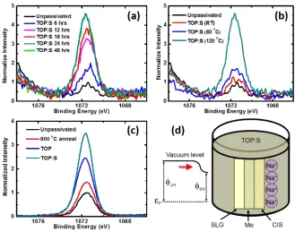
Figure 4.1 XPS and PL measurements on CIS films before and after
TOP:S passivation.(a) Normalized PL intensity for unpassivated
(baseline) CIS films, and films with passivation times up to 48
hours. (b) Normalized PL intensity for unpassivated (baseline) CIS
films, and films for passivation temperature up to 120 °C. (c,d)
Surface XPS spectra of (c) S 2s and (d) P 2p peaks for CIS thin
films with (red) and without (black) TOP:S treatment (120 °C, 24
hours)
XPS measurements were conducted on CIS films with and without the TOP:S passivation at room temperature to understand the binding state of TOP:S on passivated film surfaces. Figure 4.1(c) shows the XPS peaks of S 2p (161.8 eV) , Se 3p1/2 (166.1 eV), and 3p3/2 (160.5
spectra reveal the emergence of a small S 2p peak after passivation, which indicates that the sulfur from TOP:S binds to the film surface, presumably by forming Cu2S and In2S3. Figure 4.1(d) shows an increase in the P 2p peak as a result of the P atom in the TOP ligand interacting with dangling bonds on the film surface. In contrast to the increases in PL intensity, the increases in the intensity of S and P XPS peaks were independent of TOP:S passivation temperature, as shown in Figure 4.2, which suggests that binding of TOP:S molecules to the film surface did not cause the increase in PL.
Figure 4.2 XPS measurements showing the formation of In2S3 after
TOP:S passivation.XPS spectra of In 3d without and with TOP:S
120 °C), showing the binding of TOP:S to CIS surfaces is invariant
of temperature
4.3(d) shows a schematic of this mechanism, in which Na congregates at CIS film surface in TOP:S solution and lead to a change in surface ionization potential.
Figure 4.3 XPS measurements before and after TOP:S passivation
showing the increase in surface Na content.Surface XPS spectra of
Na 1s peak for unpassivated CIS film (baseline) and (a) films with
passivation times up to 48 hours, (b) films with passivation
temperatures up to 120 °C, and (c) SLG substrates treated with TOP
and TOP:S at 120 °C for 24 hours and annealed at 600 °C for 12
hours. (d) Schematic of increased surface Na concentration from
4.3.2 Analysis of Through-thickness Na Concentration Profile
Figure 4.4 Na concentration profile in TOP:S passivated and
as-fabricated CIS films.Representative cross-sectional STEM images
with Na concentration profiles overlaid over the images for (a)
as-fabricated and (b) TOP:S passivated CIS films. The intercepts
between the dashed lines with boxed regions show the actual
location of the measurements. The x-axis shows the average Na
Figure 4.5 Species concentration in as-fabricated CIS films. (a)
Representative STEM image of as-fabricated CIS film. Highlighted
region shows the area used for concentration mapping. (b,c,d)
Concentration maps for Na, Cu and Se measured in region
Figure 4.6 Species concentration in passivated CIS films (a)
Representative STEM image of passivated CIS film. Highlighted
region shows the area used for concentration mapping. (b,c,d)
Concentration maps for Na, Cu and Se measured in region
highlighted in (a)
4.3.3 Energetics of Na Defect Formation in Bulk CIS
(3) Na in a tetrahedral interstitial site within the CIS lattice (Natet), and (4) Na in an octahedral interstitial site within the CIS lattice (Naoct). In the simulations, a single Na atom was introduced into a 64-atom CuInSe2 unit cell, which corresponds to a Na defect density of 1.3 at.%, a magnitude similar to the surface concentration measured by EDS. All calculations in bulk CIS crystals are performed in stoichiometric CuInSe2 systems. We did not consider Na-Na “dumbbells”, where two Na-Na atoms reside on the same lattice site, in these simulations because their formation energy at various sites has been reported to follow the same trend as their single-atom counterparts.157
Figure 4.7 DFT model and results of Na defects in bulk CIS. (a):
Schematic showing various Na defects in the CIS unit cell, Na
atoms are shown in black, Cu in blue, In in red, and Se in green.
(b): Formation energy (eV) of various Na defects as a function of
Fermi energy (eV) relative to VBM. Intercepts with the dashed line
We represent and compute the total defect formation energy 𝐸𝐸𝐹𝐹 by:
𝐸𝐸𝐹𝐹 = 𝐸𝐸𝑚𝑚𝑚𝑚𝑓𝑓𝑚𝑚𝑑𝑑𝑡𝑡− 𝐸𝐸𝑏𝑏𝑚𝑚𝑒𝑒𝑘𝑘±∑ 𝑙𝑙�𝑖𝑖𝜇𝜇𝑖𝑖 +𝑞𝑞𝐸𝐸𝐹𝐹𝑚𝑚𝑚𝑚𝑚𝑚𝑖𝑖 (4.1)
where 𝐸𝐸𝑏𝑏𝑚𝑚𝑒𝑒𝑘𝑘 is the total energy of the bulk unit cell, 𝐸𝐸𝑚𝑚𝑚𝑚𝑓𝑓𝑚𝑚𝑑𝑑𝑡𝑡 is the total energy of the unit cell that contains the specific defect, 𝜇𝜇𝑖𝑖 and 𝑙𝑙�𝑖𝑖 are the chemical potential and the concentration of species 𝑖𝑖, 𝑞𝑞 is the defect charge state derived from the differences in charge states for individual species (+1 for Cu and Na, +3 for In), and 𝐸𝐸𝐹𝐹𝑚𝑚𝑚𝑚𝑚𝑚𝑖𝑖 is the system Fermi level relative to the valence band maximum (VBM). We calculated the product 𝑙𝑙�𝑖𝑖𝜇𝜇𝑖𝑖 for Cu and In as the energy of removing one Cu or In atom from the bulk unit cell, respectively. This product,
𝑙𝑙�𝑖𝑖𝜇𝜇𝑖𝑖 for Na as a point defect in the CIS system is not as readily available because Na is
The systems were relaxed in similar a fashion to the bulk calculations detailed above. The
Figure 4.8 Total energy for systems with various levels of NaCu
substitution, aligned to pristine CIS. The Dotted line shows a linear
fit of total energy vs. number of Na atoms per 64-atoms unit cell.
The Cross with a dashed line represents the energy change due to
one NaCu substitution in a CIS unit cell with 64 atoms
depend on alignment of system Fermi level, whereas system bandgap is a better representation of accuracy of calculation. Defect formation energies as a function of Fermi level are plotted in Figure 4.7(b), where the intercepts with the solid vertical line marks the mid-bandgap formation energy (0.52 eV from VBM). These results indicate that Na at a Cu lattice site, NaCu, has the lowest formation energy among all the defects types considered under most doping conditions; Na at an In lattice site, NaIn, becomes favorable under extreme n-type doping, where the Fermi level shifts to 0.9 eV above VBM.
4.3.4 Calculation of NaCu Energetics at the Film Surface
some of the Cu atoms from the stoichiometric Cu1In1Se2 unit cells (Cu content 25 at.%, designated by Cu-rich) and inserting additional In atoms in their place if needed to balance the charge, while maintaining the total number of Se atoms constant. We constructed all unit cells consistent with these compositions and chose the geometry with the lowest DFT energy as the optimal structure. We considered Cu rich and Cu-poor conditions for both surface orientations, a total of 4 cases: (1) Cu-rich (110), (2) Cu-rich (112), (3) Cu-poor (110) and (4) Cu-poor (112). Our calculations demonstrate that of all possible defect occupancy sites, the sodium-copper substitution, NaCu is the most energetically favorable defect in bulk CIS (Figure 4.7(b)). We postulate that it is also the preferred type of defect at the CIS surface because the vicinity of the free surface is unlikely to change the electron configuration of substitutional point defects in the case of NaCu and sodium-indium substitution NaIn225, while interstitial Na defects are significantly higher in formation energy compared to substitutional cases. Based on these findings, we restrict surface calculations to NaCu only; and the defect charge state 𝑞𝑞 in Equation. 4.1 becomes 0 because Na and Cu are monovalent, and the term
𝑞𝑞𝐸𝐸𝐹𝐹𝑚𝑚𝑚𝑚𝑚𝑚𝑖𝑖 vanishes.
Figure 4.9 Optimized structure of the SP(CH3)3 molecule used in
DFT calculations to simulate the effect of TOP:S passivation on
film surface. S atom is shown in yellow, P in cyan, C in brown, and
Figure 4.10 The effect of Na substitution on optimized geometry of
CIS free surface. Left: Optimized CIS unit cell with one SP(CH3)3
placed on top. Cu atoms are shown in blue, In in red, Se in green,
S in yellow, P in cyan, C in brown, and H in white. Right:
Optimized CIS unit cell with one NaCu substitution and one
SP(CH3)3 placed on top of the Na atom. The Na atom is shown in
black. In both schematics dashed line shows the direction of the
free surface, and the solid line shows the direction of fixed atomic
layer
differences among different surface conditions. Cu-poor (110) surfaces have the lowest (most favorable) formation energy at -0.05 eV, compared to 0.29 eV in the bulk. A comparison with passivated surfaces (red bar) reveals that the formation energies decrease for all surface configurations after passivation. Here significant decreases up to ~1 eV were reached for Cu-rich (110) and Cu-poor (112) cases. In all cases, the surface formation energies of NaCu are lower compared to those in the bulk, suggesting the presence of a driving force for Na diffusion towards film surfaces, which is further enhanced by TOP:S passivation. Figure 4.12 shows the atomic-level configurations of the Na defect within each CIS film surface studied, as well as the passivation molecule after surface relaxation.
Figure 4.11 Formation energy of NaCu at film surfaces with and
without TOP:S. Shaded: Formation energy (eV) of NaCu
substitution in bulk CIS taken from Figure 3(c). Blue: Formation
Cu5In9Se16, Cu-rich Cu1In1Se2, (110) and (112) orientations). Red:
Formation energy (eV) of NaCu substitution on the same surfaces
with one SP(CH3)3 placed on top
Figure 4.12 Optimized surface geometrywith SP(CH3)3 molecule.
(a): Cu-rich (110), (b): Cu-rich (112), (c): Cu-poor (110) and (d):
Cu-poor (112). Each case show parts of the surfaces containing the
NaCu substitution. Color scheme follows that of Figure 4.9. Dashed
4.4 Discussion
4.4.1 Na Distribution in the Presence of TOP:S Passivation
temperature (Figure 4.2), which implies that the adsorption of TOP:S is not temperature-limited and is unlikely to fully account for the increase in PL response after passivation.