Cascode Bulk Driven Operational Amplifier
with Improved Gain
A.V.D. Sai Priyanka 1, S. Subba Rao 2
P.G. Student, Department of Electronics and Communication Engineering, VR Siddhartha Engineering College,
Kanuru, Vijayawada, India1
Assistant Professor, Department of Electronics and Communication Engineering, VR Siddhartha Engineering College,
Kanuru, Vijayawada, India 2
ABSTRACT: In recent years, there is more demand on high-speed digital circuits at low power consumption. The main objective for Cascode bulk driven Op Amp with Improved gain is to enhance gain by employing a cascode stage in bulk driven Op Amp. Bulk driven technique is a newly adoptable technique which employed in Op Amp to reduce the threshold voltage limitation. By this technique the threshold voltage limitation is reduced, but due to low bulk trans-conductance the open loop gain is reduced. So to improve gain the cascode stage is employed in Op Amp. By this employment the gain is increased when compared to conventional bulk driven Op Amp. This paper presents a design of bulk driven input stage of Operational Amplifier using a standard 130nm CMOS Technology. The Results exemplify that gain is 60 dB, the 3-dB Bandwidth is 1.2 MHz. under single supply of 0.65V.
KEYWORDS:Bulk driven technique, Cascode stage, Bulk driven Op amp (operational amplifier).
I. INTRODUCTION
Amplifiers which operate at low power supply would consummate for biomedical and sensor applications. The combative scaling of CMOS technologies to nanometer dimensions necessitates lessening the power supply voltage accordingly in integrated circuits (ICs). With the development of these ICs, battery-powered electronic devices have become much smaller in size and are capable of operating much overlong than ever before. However, compared to their digital counterparts, analog circuits such as Operational Amplifiers (Op Amps) usually avoid the employment of advanced CMOS process technologies since the short channel devices commonly provide worse offset, larger leakage current and smaller output impedance compared to their long channel devices. In addition, the low-voltage operation further muddles the designs of analog circuits due to bounded signal swings.
Prevailing amplifiers require power supply voltages at least equal to the addition of magnitude of the largest threshold voltages of PMOS or NMOS transistors and necessary signal swing [1]. Unfortunately, with the scaling of power supply voltages, the threshold voltage in the deep sub-micron CMOS processes is not shortened [2]. As a result, to design ultra-low voltage amplifiers with sufficient signal swings, novel circuit techniques are required.
Without employing expensive transistors, low voltage methods have been developed, such as designs utilizing bulk-driven MOSFETs [1] or floating-gate MOSFETs [3], sub-threshold design [4] and level shifting techniques, etc. Among them, the bulk-driven technique is optimistic and has been extensively used in recent years [5]–[7].
structures are conferred and analysed. A low-voltage bulk driven op amp is conferred and modified to cascode bulk driven op amp by providing a cascode stage and afford proper biasing for these input stages. As a result, the effective trans-conductance of cascode bulk-driven input stage is decidedly improved when compared to their conventional counterparts. Finally, a low-voltage cascode bulk driven operational amplifier is implemented with improved UGBW and open loop gain.
Section II of this paper provides an outline of the conventional driven technique. In Section III, proposed bulk-driven input stages with improved effective trans-conductance are introduced and analysed. The simulation results for all designs are executed using a Pyxis schematic editor 130-nm technology is discussed in section V. This paper concludes with conclusion VI.
II. RELATED WORK
As the unit size of modern CMOS processes are scaled down, the maximum allowable power supply continuously decreases, but the threshold voltage does not diminish with the same rate. Bulk driven technique uses body terminal as signal input. This technique is promising method as it achieves enhanced performance by limiting threshold voltage method. For a long-established MOSFET, it is obligatory to meet the requirement of VGS > Vth in order to make the MOSFET function in the saturation region. In contrast, the bulk-driven technique allows even compact voltage to set at the input terminal, but still precipitate saturation voltage at the output. The operation of the bulk-driven MOSFET is similar to the operation of JFET [1]. Once the inversion layer under the gate of the transistor is formed by ample gate-to-source biasing voltage, the channel current can be adjusted by varying the bulk-gate-to-source junction potential. This bulk driven operation abolish the threshold voltage limitation of the gate-driven MOSFETs where the bulk-to-source junction can operate under negative bias, zero bias or marginally positive bias conditions.
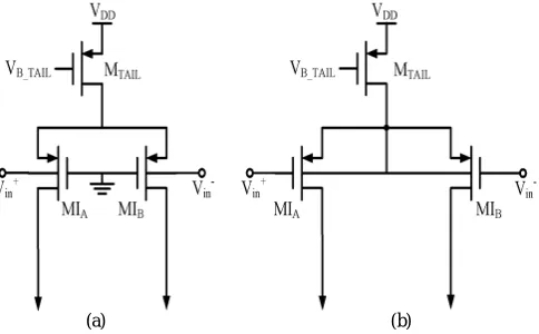
(a) (b)
Fig. 1(a) Traditional bulk driven Differential amplifier; (b) Conventional gate driven Differential amplifier
Fig. 1(a) shows one distinctive application of the bulk-driven PMOS in a differential amplifier. The gates of the bulk driven transistors are biased by a negative power supply to certify that both devices are operating in the saturation region. By scaling down the threshold voltage, the input common mode range becomes wider and the most notable issue related to the bulk-driven differential pairs is its small bulk trans-conductance (gmb) compared to the gate trans-conductance (gm). The relation between gmb and gm is expressed as
η=g
g =
γ
2 2φ + V (1)
depends on the bulk-to-source voltage and other peculiar process parameters. The bulk-driven MOSFET trans-conductance (gmb) can overreach the gate-driven MOSFET trans-conductance (gm) if
VBS≥ 2φf - 0.25 (2)
One of the basic building blocks in analog circuits is a differential amplifier. The bulk-driven differential pair (BDDP) is shown in Fig.1 (a) the gates of both devices are tied to more positive voltages for NMOS input transistors and more negative voltage for PMOS input transistors so that an inversion layer is formed as channel beneath the gate of particular MOSFET.
III. PROPOSED BULK-DRIVEN OP AMP
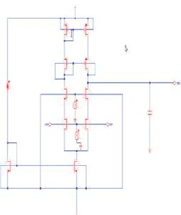
The two-stage operational trans-conductance amplifier consists of following stages, the first stage is the Bulk-driven differential stage, which is comprised of NMOS input devices M1 and M2 and the current mirror M3 and M4 is acting as an active load. The second stage is a common source amplifier which enhances the gain of Op-amp. M6 and M7 transistors formed as a common source stage. The gate-source voltage fixed to a certain value is sufficient to turn on the transistor and then the operation of the bulk-driven MOS transistor becomes a depletion type. Input bulk-source voltage is applied to the bulk terminal of the MOS transistor to modulate the channel current. Conventional bulk driven operational trans-conductance amplifier is designed and depicted in Fig. 3.1. The simulation results of the bulk driven Op amp is shown below. Transient, AC analysis, simulations have been made for bulk driven Op amp. The gain obtained by this bulk driven Op amp is 40 dB.
The Telescopic cascode Op amp consists of the bulk-driven cascode differential stage with NMOS input devices M1, M2 and the cascaded transistors M3 and M4. The current mirror M5 and M6 is acting as an active load whereas M7 and M8 are cascaded transistors. By setting the gate-source voltage to a sufficient value, it turns ON the transistor and the operation of the bulk-driven MOS transistor becomes a depletion type. Input bulk-source voltage is applied to the bulk terminal of the MOS transistor then the channel current gets modulated. Telescopic cascode OTA with bulk driven input transistors is designed. By employing a cascode stage in OTA the output resistance (ro) gets increased so that the gain enhanced. The cascode stage has high input impedance, higher output impedance, high bandwidth and higher gain. The simulation results of the Fig. 3.3 schematic, i.e. telescopic cascode bulk driven opamp is shown below. Transient, AC analysis, simulations has been made for telescopic cascode bulk driven op amp. According to transient analysis the peak to peak output voltage is 1volt. The gain obtained by this telescope cascode bulk driven op amp is 50 dB.
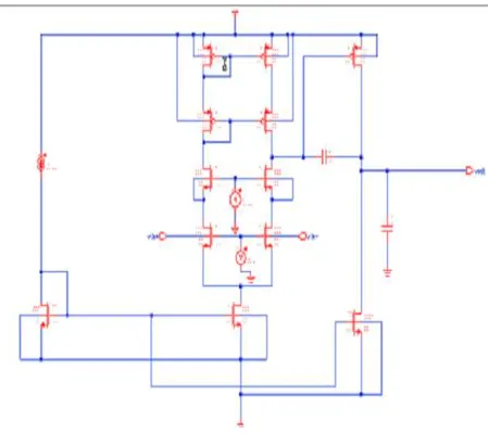
The Cascode bulk driven Op amp consists of two stages, the first stage is Bulk-driven cascode differential stage, which is comprised of NMOS input devices M1 and M2 and the cascaded transistors M3 and M4; The current mirror M5 and M6 is acting as an active load whereas M7 and M8 are cascaded transistors. By setting the gate-source voltage to a sufficient value to turn ON the transistor, then the working of bulk-driven MOS transistor becomes a depletion type. Input bulk-source voltage is applied to the bulk terminal of the MOS transistor to modulate the channel current. Cascode bulk driven operational trans-conductance amplifier is designed and depicted in Fig. 3.6. The gain can be increased further by employing the second stage i.e. common source stage into conventional bulk driven Op amp. Common source p type MOSFET is opted for this proposed design because of its higher swing. The gain of proposed design enhances by employing both cascode stage and common source stage. Transient, AC analysis, simulations has been made for cascode bulk driven Op amp are shown below. According to transient analysis, the peak to peak output voltage is 3.3volts. The gain obtained by this telescope cascode bulk driven op amp is 65 dB.
IV. SIMULATION RESULTS
are converted to the output currents. By the current mirror load, the output currents of first stage act, as the input currents which converted to output voltages. The output voltage acts as the input, which converts into output current by common source MOSFET. The input current reshapes into the output voltage (Vout) by current sink load.
Fig. 3.1 Schematic of bulk driven Op amp
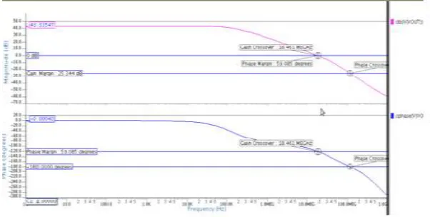
The below Fig. 3.2 is the AC response used for observing open loop gain, Unity Gain Bandwidth (UGB) and the Phase Margin of the circuit. No DC bias potential is applied to bulk terminals. The bias voltage is applied to gate terminals to bring the transistor in the saturation region. The output was taken between single end and ground terminals.The gain obtained by this bulk driven Op amp is 40 dB.
Fig. 3.2 AC analysis of bulk driven op amp
Fig. 3.3 Schematic of telescopic cascode bulk driven op amp
The transient analysis of telescopic cascode bulk driven op amp is shown below in Fig. 3.4. We get the output swing (peak to peak) 1.02V to an input signal of swing 0.02V for which the output signal swing is not distorted. The gain can be calculated by the ratio of output peak to peak voltage to input peak to peak voltage. By this process the gain of this design is 50 dB.
Fig. 3.4 Transient analysis of telescopic cascode bulk driven op amp
Fig. 3.5 AC analysis of telescopic cascode bulk driven opamp
Cascode bulk driven operational amplifier is designed and depicted in Fig. 3.6. The gain can be increased further by employing the second stage, i.e. common source stage into conventional bulk driven Op amp. Transient, AC analysis, simulations has been made for cascode bulk driven Op amp are shown below. The cascode stage has high input impedance, higher output impedance, high bandwidth and higher gain. Common source p type MOSFET is opted for this proposed design because of its higher swing. The gain of proposed design enhances by employing both cascode stage and common source stage.
Fig. 3.6 Schematic of proposed cascode bulk driven op amp
Fig. 3.7 Transient analysis of telescopic cascode bulk driven opamp
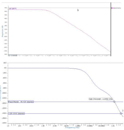
The below Fig. 3.8 is the AC response used for observing open loop gain, Unity Gain Bandwidth (UGB) and the Phase Margin of the circuit. No DC bias potential is applied to bulk terminals. The bias voltage is applied to gate terminals to bring the transistor in the saturation region. The output was taken between single end and ground terminals. The gain obtained by this bulk driven Op amp is 65 dB. To make the system stable, the compensation capacitor (CC) should be greater than the 0.22 of the load capacitors (CL). Gain and phase margin indicates relative stability of a circuit.
Fig. 3.8 AC analysis of cascode bulk driven opamp
Table I Feature comparisons of different op amp topologies
V. CONCLUSION
This paper mainly focuses on the gain in dB. By employing a bulk driven technique, there is no threshold voltage limitation, but the gain will be diminished. So to improve gain a cascode stage is employed in the first stage of an operational amplifier. By this about 50% of the gain has improved for proposed cascode bulk driven Op amp when compared to conventional bulk driven Op amp.
REFERENCES
[1] B. J. Blalock, P. E. Allen, and G. A.Rincon-Mora, “Designing 1-V OpAmps using standard digital CMOS technology,” IEEE
Transaction .Circuits Syst. II, Analog Digit. Signal Process, vol. 45, no. 7, pp. 769–780, Jul.1998.
[2] S. S. Rajput and S. S. Jamuar, “Low voltage analog circuit design techniques,”IEEE Circuits System Mag., vol. 2, no. 1, pp. 24–42, 2002.
[3] P. Hasler and T. S. Lande, “Overview of floating gate devices, circuits and systems,” IEEE Trans. Circuits Syst. II, Analog Digit. Signal
Process, vol. 48, pp. 1–3, Jan. 2001.
[4] Y. Hga, H. Zare-Hoseini, L. Berkovi, and I. Kale, “Design of a 0.8 volt fully differential CMOS OTA using the bulk-driven technique,” in
IEEE Int. Symp. On Circuits and Systems, May 2005, pp. 220–223.
[5] S.-W. Pan, C.-C. Chuang, C.-H. Yang, and Y.-S. Lai, “A novel OTA with dual bulk-driven input stage,” in Proc. IEEE Int. Symp. Circuits
Syst., June 2009, pp. 21–24.
[6] T. Lehmann and M. Cassia, “1-V power supply CMOS cascode amplifier,”IEEE J. Solid-State Circuits, vol. 36, no. 7, pp. 1082–1086,
2001.
[7] A. Guzinski, M. Bialko, and J. C.Matheau, “Body driven differential amplifier for application in continuous-time active C-filter,” in Proc.
ECCD, 1987, pp. 315–319.
[8] T. Stockstad and H. Yoshizawa, “A 0.9-V 0.5 rail-to-rail CMOS operational amplifier,” IEEE J. Solid-State Circuits, vol. 37, no. 3, pp.286–
292, 2002.
[9] G. Raikos and S. Vlassis, “0.8 V bulk-driven operational amplifier,”Analog Integr. Circuits Signal Process, vol. 63, no. 3, pp. 425–432,
2010.
[10] A. P. Chandrakasan, S. Sheng. and R. W. Brodersen, “ Low-power CMOS digital design,” IEEE J Solid-State Circuits, vol. 27, pp.473-484,
Apr. 1992.
[11] M. Nagata, “Limitation, innovations, and challenges of circuits and devices into a half micrometer and beyond,” IEEE J Solid-State Circuits,
vol. 27, pp. 465-472, Apr. 1992.
[12] S. Sakurai and M. Ismail, “Robust design of rail-to-rail CMOS operational amplifiers for a low power supply voltage,” IEEE J. Solid-State
Circuit, vol. 31, no. 2, pp. 146-156, Feb. 1996.
[13] D. M. Monticelli, “ A qquad CMOS single-supply opamp with rail-to-rail output swing,” IEEE J. Solid-State Circuits, vol. SSC-21, no. 6,pp.
1026-1034, Dec. 1996.
Topology Gain dB
UBW PHASE MARGIN
Vpeak-peak
Conventional Bulk driven
Opamp
40 18.4 MHz
59.08 degrees 0.8V
Telescopic Cascode bulk driven Opamp 50.02 0.3 GHz
72 degrees 1V
Cascode bulk driven Opamp
65 1.2 GHz