ISSN(Online) : 2319-8753 ISSN (Print) : 2347-6710
I
nternational
J
ournal of
I
nnovative
R
esearch in
S
cience,
E
ngineering and
T
echnology
(An ISO 3297: 2007 Certified Organization)
Vol. 5, Issue 4, April 2016
Design, Analysis and Implementation of Solar
Power Optimizer for DC Distribution System
Dr.V.Balakrishna Reddy
Professor, Department of EEE, Vijay Rural Engineering College, Nizam Bad, Telangana, India
ABSTRACT: This paper proposes a high step-up solar power optimizer (SPO) that efficiently harvests maximum energy from a photovoltaic (PV) panel then outputs energy to a dc-micro grid. Its structure integrates coupled inductor and switched capacitor technologies to realize high step-up voltage gain. The leakage inductance energy of the coupled inductor can be recycled to reduce voltage stress and power losses. A low voltage rating and low-conduction resistance switch improves system efficiency by employing the incremental conductance method for the maximum power point tracking (MPPT) algorithm. Because of its high tracking accuracy, the method is widely used in the energy harvesting of PV systems. The simulation is carried over by the MATLAB-SIMULINK software. The hardware design is implemented by PIC16F877A controller circuit.
KEYWORDS: MPPT,PV Bus, SPO,CCM,Vin,Vo,Fs
I. INTRODUCTION
GENERAL
A power optimizer is a DC to DC converter technology developed to maximize the energy harvest from solar photovoltaic or wind turbine systems. They do this by individually tuning the performance of the panel or wind turbine through maximum power point tracking, and optionally tuning the output to match the performance of the string inverter. Power optimizers are especially useful when the performance of the power generating components in a distributed system will vary widely, differences in equipment, shading of light or wind, or being installed facing different directions or widely separated locations. Power optimizers for solar applications, can be similar to microinverters, in that both systems attempt to isolate individual panels in order to improve overall system performance. A microinverter essentially combines a power optimizer with a small inverter in a single case that is used on every panel, while the power optimizer leaves the inverter in a separate box and uses only one inverter for the entire array. The claimed advantage to this "hybrid" approach is lower overall system costs, avoiding the distribution of electronics.
SCOPE OF THE PROJECT
The proposed converter has the following features: 1) its voltage conversion ratio is efficiently increased by using the switched capacitor and coupled inductor techniques; 2) the leakage inductance energy of the coupled inductor can be recycled to increase efficiency, and the voltage spike on the active switch is restrained; 3) the floating active switch isolates the PV panel’s energy during non operating conditions, thereby preventing any potential electric hazard to humans or facilities. The MPPT control algorithm exhibits high-tracking efficiency; hence, it is widely used in the energy harvesting of PV systems.
EXISTING SYSTEM
ISSN(Online) : 2319-8753 ISSN (Print) : 2347-6710
I
nternational
J
ournal of
I
nnovative
R
esearch in
S
cience,
E
ngineering and
T
echnology
(An ISO 3297: 2007 Certified Organization)
Vol. 5, Issue 4, April 2016
EXISTING SYSTEMS TECHNIQUE:
In the traditional grid-connected PV inverters, either a line frequency or a high-frequency transformer is utilized to provide a galvanic isolation between the grid and the PV panels. For a typical PV array, the output voltage is relatively low, and a high voltage gain is obligatory to realize the grid-connected function.
PROPOSED SYSTEM
A solar power optimizer (SPO) was developed as an alternative to maximize energy harvest from each individual PV module. An SPO is used as a dc–dc converter with maximum power point tracking (MPPT), which increases PV panel voltage to optimum voltage levels for a dc microgrid connection. The SPO attempts to improve the use of distributed renewable resources and lower system cost. It may also potentially improve the efficiency of PV systems, has an antishadow effect, and can monitor the status of PV modules.
PROPOSED SYSTEM TECHNIQUE
The proposed SPO’s configuration is based on a high step-up dc–dc converter with an MPPT control circuit. The converter includes a floating active switch S and a coupled inductor T1 with primary winding N1, which is similar to the input inductor of a conventional boost converter capacitor C1, and diode D1 recycle leakage inductance energy from N1. Secondary winding N2 is connected to another pair of capacitors, C2 and C3, and to diodes D2 and D3. Rectifier diode D4 connects to output capacitor Co and load R. The duty ratio is modulated by the MPPT algorithm, which uses the incremental conductance method is employed in the proposed SPO.
ADVANTAGES OF PROPOSED TECHNIQUE Improve voltage level.
Recycling the leakage inductance energy.
Reduce the voltage stress on the switch.
Improved power capacity.
II. CIRCUIT DIAGRAM
Circuit Diagram Proposed
Fig.1
The proposed SPO is shown in Fig. 1; its configuration is based on a high step-up dc–dc converter with an MPPT control circuit. The converter includes a floating active switch S and a coupled inductor T1 with primary winding N1 , which is similar to the input inductor of a conventional boost converter capacitor C1 , and diode D1 recycle leakage inductance energy from N1 . Secondary winding N2 is connected to another pair of capacitors, C2 and
ISSN(Online) : 2319-8753 ISSN (Print) : 2347-6710
I
nternational
J
ournal of
I
nnovative
R
esearch in
S
cience,
E
ngineering and
T
echnology
(An ISO 3297: 2007 Certified Organization)
Vol. 5, Issue 4, April 2016
modulated by the MPPT algorithm, which uses the perturb and observer method that is employed in the proposed SPO. It detects PV module voltage Vpv and current Ipv to determine the increase and decrease in the duty cycle of the dc converter. Therefore, the MPP can be obtained by comparing instantaneous conductance I/V and incremental conductance dI/dV.
The proposed converter has the following features:
1) its voltage conversion ratio is efficiently increased by using the switched capacitor and coupled inductor techniques; 2) The leakage inductance energy of the coupled inductor can be recycled to increase efficiency, and the voltage spike on the active switch is restrained;
3) The floating active switch isolates the PV panel’s energy during non operating conditions, thereby preventing any potential electric hazard to humans or facilities. The MPPT control algorithm exhibits high-tracking efficiency;
Operation Modes
The operating principles for continuous conduction mode (CCM) and discontinuous conduction mode (DCM) are presented in detail and shown in schematic form in Fig.1.
A. CCM OPERATION
The CCM operating modes are described as follows.
Mode I [t0 , t1 ]: During this interval, switch S and diodes D2 and D3 are conducted; diodes D1 and D4 are turned OFF. The current flow path is shown in Fig.(a). Magnetizing inductor Lm continues to release energy to capacitors C2 and C3 through secondary windingN2 of coupled inductor T1 . Leakage inductance Lk 1 denotes the stored energy from source energy Vin . The energy that is stored in capacitor Co is constantly discharged to load R. This mode ends when increasing iLk1 is equal to decreasing iLm at t = t1.
Mode II [t1 , t2 ]: During this interval, switch S and diode D4 are conducted. Source energy Vin is serially connected to
C1, C2 , and C3 , and secondary winding N2 ; Lk2 discharges the energy that is stored in charge output capacitor Co
ISSN(Online) : 2319-8753 ISSN (Print) : 2347-6710
I
nternational
J
ournal of
I
nnovative
R
esearch in
S
cience,
E
ngineering and
T
echnology
(An ISO 3297: 2007 Certified Organization)
Vol. 5, Issue 4, April 2016
Mode III [t2 , t3 ]: During this transition interval, switch S and diodes D2 and D3 are turned OFF, and diodes D1 and
D4 are conducted. The current flow path is shown in Fig.(c). The energy stored in leakage inductance Lk 1 instantly flows through the diode D1 to charge capacitor C1 . The energy is released to magnetizing inductor Lm through coupled inductor T1 , which is serially connected to C1, C2 , and C3 , and secondary winding N2 ; Lk2 discharges the energy that is stored in charge output capacitor Co and loads R. This mode ends when decreasing iLk1 is equal to increasing iLm at t = t3.
Mode IV [t3 , t4 ]: During this interval, switch S and diode D4 are turned OFF, and diodes D1,D2 , and D3 are conducted. The current flow path is shown in Fig.(d). Leakage inductance Lk 1 continues to release energy to charge capacitor C1 through diode D1 . Magnetizing inductor Lm through coupled inductor T1 transfers energy to capacitors
ISSN(Online) : 2319-8753 ISSN (Print) : 2347-6710
I
nternational
J
ournal of
I
nnovative
R
esearch in
S
cience,
E
ngineering and
T
echnology
(An ISO 3297: 2007 Certified Organization)
Vol. 5, Issue 4, April 2016
Mode V [t4 , t5 ]: During this interval, diodes D2 and D3 are conducted. The current flow path is shown in Fig.(e). Magnetizing inductor Lm constantly transfers energy to secondary winding N2 , and charges capacitors C2 and C3 . The energy that is stored in capacitor CO is constantly discharged to load R. This mode ends when switch S is turned ON at the beginning of the next switching period.
B. DCM OPERATION
ISSN(Online) : 2319-8753 ISSN (Print) : 2347-6710
I
nternational
J
ournal of
I
nnovative
R
esearch in
S
cience,
E
ngineering and
T
echnology
(An ISO 3297: 2007 Certified Organization)
Vol. 5, Issue 4, April 2016
Fig: f
Mode II [t1 , t2 ]: During this transition interval, switch S and diodes D2 and D3 are turned OFF, and diodes D1 and
D4 are conducted. The current flow path is shown in Fig. 6(b). The energy stored in leakage inductance Lk 1 instantly flows through the diodeD1 to charge capacitor C1 ; this energy is also released to magnetizing inductor Lm through the coupled inductor T1 series that is connected to C1, C2 , and C3 , secondary winding N2 , and Lk2 to charge output capacitor Co and load R. This mode ends when decreasing iD4 is zero at t = t2.
Fig: g
ISSN(Online) : 2319-8753 ISSN (Print) : 2347-6710
I
nternational
J
ournal of
I
nnovative
R
esearch in
S
cience,
E
ngineering and
T
echnology
(An ISO 3297: 2007 Certified Organization)
Vol. 5, Issue 4, April 2016
Fig: h
Mode IV [t3 , t4 ]: During this interval, switch S, diodes D1 and D4 are turned OFF, and diodes D2 and D3 are conducted. The current flow path is shown in Fig. 6(d).Magnetizing inductor Lm constantly transfers energy to secondary winding N2 and charges capacitors C2 and C3 . The energy that is stored in capacitor Co is constantly discharged to load R. This mode ends
ISSN(Online) : 2319-8753 ISSN (Print) : 2347-6710
I
nternational
J
ournal of
I
nnovative
R
esearch in
S
cience,
E
ngineering and
T
echnology
(An ISO 3297: 2007 Certified Organization)
Vol. 5, Issue 4, April 2016
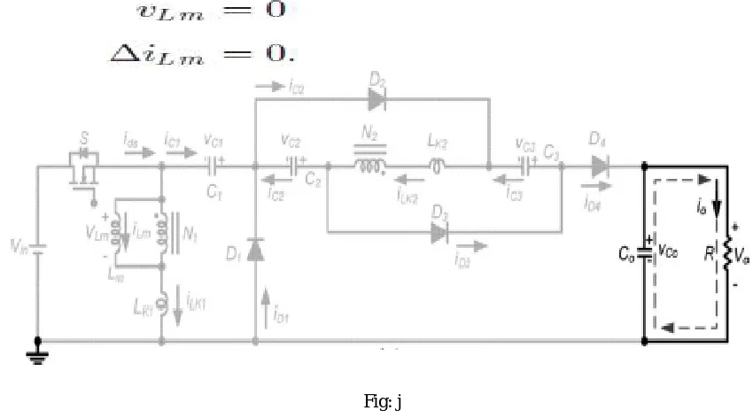
Mode V [t4 , t5 ]: During this interval, the switch and all the diodes are turned OFF. The current flow path is shown in Fig. 6(e). The energy that is stored in capacitor CO is constantly
discharged to load R. This mode ends when switch S is turned ON at the beginning of the next switching period.
Fig: j
III. SIMULATION RESULTS
TECHNIQUES USED
In the traditional grid-connected PV inverters, either a line frequency or a high-frequency transformer is utilized to provide a galvanic isolation between the grid and the PV panels. For a typical PV array, the output voltage is relatively low, and a high voltage gain is obligatory to realize the grid-connected function.
ISSN(Online) : 2319-8753 ISSN (Print) : 2347-6710
I
nternational
J
ournal of
I
nnovative
R
esearch in
S
cience,
E
ngineering and
T
echnology
(An ISO 3297: 2007 Certified Organization)
Vol. 5, Issue 4, April 2016
OPEN LOOP CIRCUIT OF SOLAR POWER OPTIMIZER
INPUT VOLTAGE WAVEFORM
ISSN(Online) : 2319-8753 ISSN (Print) : 2347-6710
I
nternational
J
ournal of
I
nnovative
R
esearch in
S
cience,
E
ngineering and
T
echnology
(An ISO 3297: 2007 Certified Organization)
Vol. 5, Issue 4, April 2016
CLOSED LOOP CIRCUIT OF SOLAR POWER OPTIMIZER
OUTPUT VOLTAGE WAVEFORM
OUTPUT CURRENT WAVEFORM
IV. CONCLUSION
APPLICATIONS
High voltage application.
Tele communication.
ISSN(Online) : 2319-8753 ISSN (Print) : 2347-6710
I
nternational
J
ournal of
I
nnovative
R
esearch in
S
cience,
E
ngineering and
T
echnology
(An ISO 3297: 2007 Certified Organization)
Vol. 5, Issue 4, April 2016
FUTURE SCOPE
The system can be extended for more voltage range. Increase in more voltage range will increases the voltage gain and efficiency of the converter system. The output DC voltage can be inverted and we can use the AC loads also.
REFERENCES
1. W. Yu, J.-S. Lai, H. Qian, and C. Hutchens, “High-efficiency MOSFET inverter with H6-type configuration for photovoltaic non isolated ac-module applications,” IEEE Trans. Power Electron., vol. 26, no. 4, pp. 1253–1260, Apr. 2011.
2. L. Gao, R. A. Dougal, S. Liu, and A. P. Iotova, “Parallel-connected solar PV system to address partial and rapidly fluctuating shadow conditions,” IEEE Trans. Ind. Electron., vol. 56, no. 5, pp. 1548–1556, May 2009.
3. R. Gules, J. De Pellegrin Pacheco, H. L. Hey, and J. Imhoff, “A maximum power point tracking system with parallel connection for PV stand-alone applications,” IEEE Trans. Ind. Electron., vol. 55, no. 7, pp. 2674–2683, Jul. 2008.
4. B. Liu, S. Duan, and T. Cai, “Photovoltaic dc-building-module-based BIPV system: Concept and design considerations,” IEEE Trans. Power Electron., vol. 26, no. 5, pp. 1418–1429, May 2011.