Error detection and correction technique for
Memory applications
Mr. J.V.PrabhakarRao1, J. Naveen2
1Assistant professor, Department of ECE, Adams engineering College, Khammam Telangana. 2
M-Tech Student Department of ECE, Adams engineering College, Khammam Telangana .
Abstract: In Advanced digital communication, the testing of Memory System is more complicated. As the technology, dimensions and operating voltages of the computer electronics are reduced to satisfy the consumer’s which leads to soft errors. The detection and correction of soft errors in the memory system is more susceptible. To protect memory cells from soft errors, we need more Advanced Errors correction codes. One-step Majority of Logic Decodable codes is suitable for Memory Application to detect and correct large number of errors during communication. One type of Euclidean Geometry Low – Density Parity Check (EG-LPDC) Codes are used for Error correction, because it has fault- secure detector capability. In this paper, an Enhanced Majority Logic Decoder/Detector (MLDD) is proposed to detect silent data errors (SDE) using additional logic and in order to reduce the area of Majority gate, the Sorting Network is designed. Thus, the proposed Method reduces the decoding time, area and power consumption. Hence the proposed Method Simulation Results are Shown as Power saving & Area Utilization compared to existing Method (One-step Majority of Logic Decodable codes).
Keywords: Majority Logic Decoder, EG-LPDC, Registers, Counters, Soft Errors, Silent Data Errors (SDE).
1. INTRODUCTION
Now a day, digital communication has becoming essential part of life and a lot of data is being transferred. Many communication channels are leads to channel noise. Networks must be able to transfer data from one device to another with acceptable accuracy. For most applications, a system must guarantee that the data received are identical to the data transmitted. The corresponding data will effected by error, which is either soft error or hard error. The Hard error is represented by Hardware Mechanism. Hence the soft error is represented by corrupted data. This Project is developed for Memory Application. When the data is stored in the memory it may be affected from error, this type of error is called soft error. To detect these types of soft errors, many error correction and detection codes are needed. At any time data are transmitted from one node to the next node, they can become corrupted in passage. Many factors can alter one or more bits of message. Some application required a mechanism for detecting and correcting large number of errors. Data can be corrupted during transmission. Some application are required that errors can be detected and corrected.
There are different methods to detect and correct errors to keep secure and accuracy data communication. Some applications can tolerate a small level of errors. For example, random errors in audio or video transmission may be tolerable, but when transfer text; we expect a very high level of accuracy.
Type of Errors
The error is soft because it will change the logic value of memory cells without damaging the circuit or device. The soft errors referred as a Single Event Error/Upset (SEU).If the radiation event is of high energy, more than a single bit may be affected by error, i.e. Multi Bit Error/Upset (MBU) [2].For reliable communication, errors must be detected and corrected. Some multi-bit error correction codes are BCH codes, Reed Solomon codes but in the following algorithm, it is very difficult and complexity. These codes can correct a
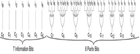
Figure1.General memory system with MLD
This method did not detect the silent data error.The general schematic of memory system implemented with majority logic decoder is shown in figure1.Initially the data words are encoded and then it fed in to the memory. When the memory is read, the corresponding code word is stored in the cyclic shift register with in a Majority Logic Decoder circuit (MLD) before sent to the output. In this decoding process, the code word is corrected if there is l bit or more than 1bit change in the data word stored in the memory.The proposed enhanced MLDD method uses additional error detection technique to detect the silent data error (SDE) in MLDD. To produce the accurate result of MLDD, this addition logic is used to detect the error, which is not detected by the first three iteration of the MLDD. To reduce the number of gates in the majority gate, a sorting network is used. Thus reduces the area of the majority gate and also reduces the power consumption. The main description of this paper is organized as follows. Section II gives an a overview of existing system of Serial one-step Majority Logic decoding; Section III presents the proposed novel improved ML decoder/detector (MLDD) using Euclidean Geometry Low Density Parity Check Codes (EG-LDPC); Section IV deal with results and discussion for proposed method with RTL Schematics, Simulation Results and comparison table between Existing and proposed Method and power consumption; Finally, Section VI deals with Conclusions.
EXISTING SYSTEM
These section deals with the Existing method that is Serial One Step Majority Logic Decoder of EG-LPDC used for error detection and correction. This Method detects if the code word is error. The disadvantage of this method is, it will take 15 cycles to detect and correct the entire code. when there are no errors in the data, decoding process will end without completing the rest of cycles and directly sent to the output of MLD. Hence most of the code word is free from error and the decoding time is greatly reduced.
Serial One-Step Majority Logic Decoder
The Serial one Step Majority Logic Decoder of EG-LPDC, Majority-logic is a simple and effective decoder capable of correcting multiple bit flips depending on the number of parity check sum equations.
It consists of four parts: 1) a cyclic shift register; 2) an XOR matrix; 3) a majority gate;
4) an EXOR gate for error correction, as shown in figure2.
Figure 2. Structure of an encoder circuit for the EG-LDPC code In one step majority logic decoding [1], initially the code word is loaded in to the cyclic shift register. Then the check equations are computed. The resulting sums are then forwarded to the majority gate for evaluating its correctness. If the number of 1’s received in is greater than the number of 0’s which means that the current bit under decoding is wrong, and a signal to correct it would be triggered. Otherwise the bit under decoding is correct and no extra operations would be needed on it. In next, the content of the registers are rotated and the above procedure is repeated until codeword bits have been processed.
Figure 3. Serial one-step majority logic corrector for EG-LDPC code
Finally, the parity checksums should be zero if the code word has been correctly decoded. In this process, each bit may be corrected only once, As a result, the decoding circuit is simple, but it require as long decoding time if the code word is large. Thus, by one- step majority-logic decoding, the code is capable of correcting any error pattern with two or few errors. For example, for a code word of 15-bits, the decoding would take 15 cycles, which would be excessive for most applications. The Main disadvantage of serial one-step Majority Logic decoder of EG-LPDC it will take 15 cycles to detect and correct the entire code word. If the code word is large, the decoding process of serial one-step Majority Logic Decoder of EG-LPDC is low. The Speed of the operation is also low and time delay is more.
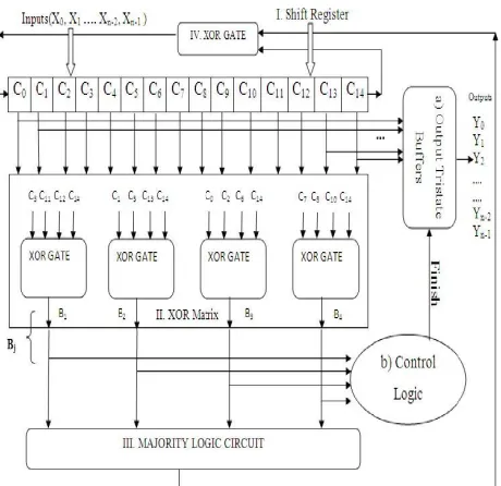
Figure 4. Schematic of a memory system with MLDD The proposed method is developed in order to overcome the drawback of serial one step Majority Logic Decoder of EG-LPDC, The Proposed method Schematic for 15 bit code word is shown in fig 4.Initailly the following code word from Memory is load in to the cyclic shift register. Then the following code is fed into the XOR Matrix for check sum. If the following code word contains error then it performs decoding process to detect and correct the error in the code word. The main advantage of proposed method is it will correct upto five error within three iteration. The proposed version uses the same decoding algorithm as the one in plain ML decoder version. The advantage is that, proposed method stops intermediately in the third cycle when there is no error in data read, [2] as illustrated in Figure. 4, instead of decoding it for the whole codeword size of N. The xor matrix is evaluated for the first three cycles of the decoding process, and when all the outputs {Bj} is “0,”the codeword is determined to be error-free and forwarded directly to the output. On other hand, the proposed method would continue the whole decoding process to eliminate the errors [2] if the {Bj} contain at least a “1” in any of the three cycles. we can clearly understand by seeing the below flow chart of figure 3 figure 3.The proposed Method will detect five errors within the three iterations.
A detailed schematic of the proposed design for 15 bit code word is shown in Figure 4. The figure shows the basic ML decoder with a 15-tap shift register, an XOR array to calculate the orthogonal parity check sums and a majority logic circuit which will decide whether the current bit under decoding is erroneous and the need for its inversion. The plain ML decoder [2] shown in Figure 1 is also having the same schematic structure up to this stage. The additional hardware intended for fault detection illustrated are: a) the control logic unit and b) the output tristate buffers. The control unit triggers a finish flag when there is no errors are detected in data read. The output tristate buffers are always in high impedance state until the control unit sends the finish signal so that the current values are directly forwarded to the output from the shift register.
Figure 5. Schematic of the proposed MLDD for 15 bit code word. a) Control logic b) Output tristate buffers
The control logic shown along with proposed Enhanced Majority Logic Decoder/Detector schematic [2] is illustrated in Figure 4.Hence the proposed control unit is shown in below Figure 5.The detection process is managed by the control unit. For distinguishing the first three iterations of the Majority Logic decoding, a counter is used in control unit as shown in figure 5, which counts up to three cycles. The control unit evaluates the output from xor matrix {Bj} by giving it input to the OR 1 gate. This output value is fed to two shift registers which the results of the previous stages stored in it. The values are shifted accordingly. The third coming input is directly forwarded to the OR 2 gate and finally all are evaluated in the third cycle in the OR 2 gate. If the result is “0,” a finish signal is send by the FSM (Finite State Machine) which indicates that the processed code word is error-free, then it send the finish signal to tristate buffer. Hence the following codeword in the register is directly fed to the output. The ML decoding process runs until the end, if the result is “1”.
RESULTS
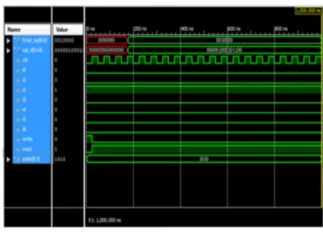
Hence the simulation results and RTL Schematics of proposed system i.e. Enhanced Majority Logic Decoder/Detector is shown in below, hence the proposed method will correct up to five errors in three decoding cycles.
Figure 6. RTL schematic for the proposed design Decodable. Hence The UART BIST architecture simulation was done through the Xilinx ISE using VERILOG HDL. The data address-bit verification can also to be done through this simulation and the waveform could be verified by using the XILINX. The corresponding simulation and RTL Schematic is shown in the below figure.
Figure 7.simulation results
CONCLUSION
In this paper, the detection and correction of errors during the first iteration of serial one step Majority Logic Decoding of EG-LPDC codes has been studied. Hence the proposed method is An Enhanced Majority Logic Decoder/Detector, which will detect and correct up to five errors within three decoding cycles, if no errors are found then the decoding process will be stopped; hence the following code is directly fed to the output. Hence in the proposed system, the decoding time, power, area, delay is reduced by stopping the decoding process when no errors are detected. This papers presents the UART based BIST Architecture using VERILOG HDL. Most of the researchers have been used to implement this testing algorithm in VERILOG for stable,
compact and reliable transmission. The structural details have been recognized and it can be integrated into the chip could be easier. The UART transmission could be relatively used in all the devices for the reliable transmission of data’s from the structure where it could be converter and tested as a bit files generation. This design function can be adopted as a technical preserving data’s for communication. The BIST controller as a device uses as an efficient bit generation for the chip implementation.
REFERENCES
[1] Pedro Reviriego, Juan A. Maestro, and Mark F. Flanagan, ”Error Detection in Majority Logic Decoding of Euclidean Geometry Low Density Parity Check (EG-LDPC) Codes ”IEEE Trans. Very Large Scale Integration (VLSI) Systems, Vol.21, No.1, January2013.
[2] R.C.Baumann, “Radiation-induced soft errors in advanced semiconductor technologies, ”IEEE Trans. Device Mater. Reliab., vol.5, no.3, pp.301–316, Sep.2005.
[3] M.A.Bajura, Y.Boulghas soul, R.Naseer, S.Das Gupta, A.F.Witulski, J.Sondeen, S.D.Stans berry, J.Draper, L.W.Massengill, and J.N.Damoulakis, “Models and algorithmic limits for an ECC-based approach to hard ening sub-100-nm.
[4] SRAMs,” IEEE Trans. Nucl. Sci.,vol. 54, no.4, pp. 935–945,
Aug.2007.
[5] R.Naseer and J.Draper, “DEC ECC design to improve memory reliability insub-100nm Technologies,” Proc. IEEE IC ECS, pp.586–589, 2008.
[6] S.Ghosh and P.D.Lincoln, “Dynamic low-density parity check codes for fault-tolerant nano-scale memory,” presented at the Foundations Nano sci. (FNANO), Snowbird, Utah,2007.
[7] S.Ghosh and P.D.Lincoln, “Low-density parity check codes for error correction in nano scale memory,”SRI Computer Science Lab., Menlo Park, CA, Tech.Rep.CSL-0703,2007
[8] H.Naeimi and A.DeHon, “Fault secures encoder and decoder for memory applications, “in Proc.IEEE Int.Symp. Defect Fault Toler.VLSI Syst., 2007, pp.409–417.
[9] B.Vasic and S.K.Chilappagari, information theoretical
frame work for analysis and design of nano scale fault-tolerant memories based on low-density parity-checkcodes,” IEEETrans. Circuits Syst.I, Reg. Papers, vol.54, no.11, Nov.2007.
[11] S.Lin and D.J.Costello, Error Control Coding, 2nd ed. Engle wood Cliffs, NJ: Prentice-Hall,2004.
[12] S.Liu, P.Reviriego, and J.Maestro, “Efficient majority logic fault detection with difference- set codes for memory applications, ”IEEE Trans. Very Large Scale Integer.(VLSI) Syst., vol.20, no.1, pp.148–156, Jan.2012.
[13] R.Gallager, “Low-density parity-check codes,” IRE Trans. Information Theory, pp.21-28, Jan.1962.
Mr. J.V.PrabhakarRao was born in India. He received B.Tech degree in Electronics and communication Engineering & M.Tech PG in VLSI system design from JNTUH, Hyderabad. He is expert in VLSI Design and Digital electronics. He is currently working as An Assistant Professor in ECE Department in Adam’s Engineering College, Paloncha, Khammam, Telangana State ,India.
mail id: [email protected]
Mr. J. Naveen M.TECH (VLSI system design ) PURSUING
In Adam’s Engineering College, Paloncha, Khammam
DIST, TELANGANA, INDIA.